 Skip to content
Struggling to fit everything on your board while keeping signals clean and manufacturing happy? You’re not alone. Proper component placement is a balancing act between electrical performance, mechanical constraints, and cost.
The right way to place components on a PCB is to follow a structured workflow: start with fixed components like connectors, then position critical parts like CPUs and power ICs. Group related circuits, orient parts consistently, and ensure adequate clearance for manufacturing and thermal management to optimize performance.
Getting placement right from the start saves countless hours of routing headaches and prevents costly board respins. It's the foundation of a successful design. Let's break down the process into clear, actionable steps that will help you build a robust and reliable board every time.
What Is the Standard Workflow for PCB Component Placement?
Ever feel like you're just randomly dropping parts onto a blank layout? A systematic workflow prevents chaos, ensuring that every decision builds toward a functional, manufacturable, and reliable final product.
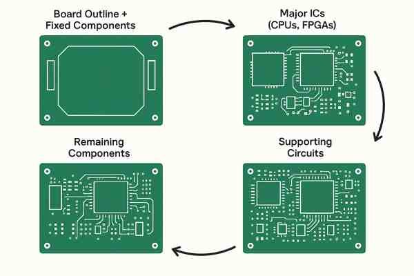
A standard workflow begins with defining the board outline and placing fixed components (connectors, mounting holes). Next, place major ICs (CPUs, FPGAs), followed by their supporting circuits. Finally, arrange the remaining components, always considering signal flow and manufacturability.
Breaking Down the Placement Workflow
A disciplined workflow is the difference between a smooth project and a nightmare of rework. On large-scale projects like the Honeywell Tuxedo Keypad, we lived by this process. It turns a complex task into a series of logical, manageable phases, ensuring nothing is overlooked.
Phase 1: Mechanical and High-Level Planning
First, you must define the physical world your board lives in. This means importing the board outline, mounting hole positions, and any fixed component locations from a mechanical drawing (like a DXF or IDF file). At the same time, you do high-level floorplanning. This is where you partition the board area into logical zones for different functions—power supply here, analog there—to prevent noisy circuits from interfering with sensitive ones.
Phase 2: Critical Component Placement
With the boundaries set, you place the most important parts. These are the anchors of your design. This includes the main processor, memory, and major power supply ICs. Their position is critical because they have the highest pin counts and influence the routing for the entire board. I always place these first to ensure the most complex connections have the shortest possible paths.
| Workflow Stage | Primary Goal | Key Actions |
|---|---|---|
| Mechanical Lock-In | Define physical boundaries. | Import board outline, place connectors and mounting holes. |
| Floorplanning | Create logical circuit zones. | Partition areas for Power, Analog, Digital, RF sections. |
| Critical Placement | Anchor the main ICs. | Place CPU, FPGA, DDR memory, key power ICs. |
| Supporting Placement | Place surrounding components. | Position bypass caps, crystals, termination resistors. |
| Final Arrangement | Position remaining parts. | Arrange all other components, optimizing for flow and density. |
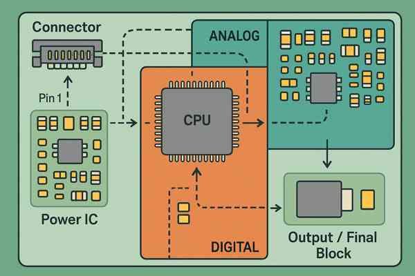
Which Components Define the Initial Placement on a New Board Layout?
Facing a blank canvas can be intimidating. Where do you start? Placing the wrong components first can box you into a corner, making routing impossible and compromising the entire design.
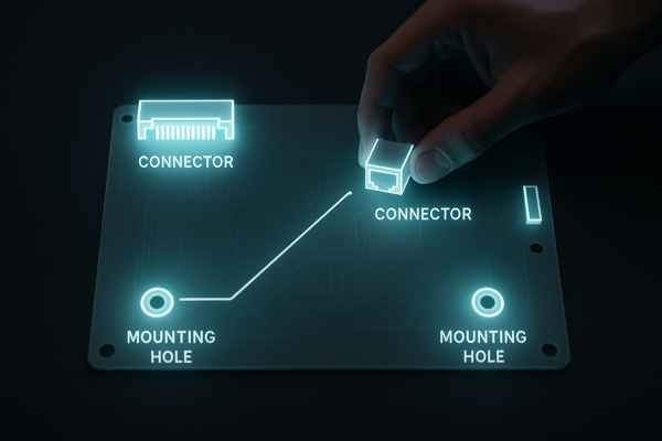
Initial placement is always defined by components with fixed positions. These include connectors, mounting holes, switches, and any other parts whose location is dictated by the mechanical enclosure or user interface. Placing these first creates the immovable framework for the rest of the layout.
Establishing Your Board's Anchor Points
Think of this initial step as setting the foundation posts for a building. These components are your non-negotiable anchor points. Their positions are determined by the outside world—how the user interacts with the device or how it mounts into a larger assembly.
The Non-Negotiable Components
These parts have their locations locked by the product's physical design. I always place these first by importing their exact coordinates from the mechanical CAD files. Trying to adjust them later is a recipe for failure, as it would require changing the product's physical enclosure.
The High-Impact ICs
After the mechanicals are locked, the next priority is the main integrated circuits. The CPU or FPGA is the "sun" and the other components are "planets" that must orbit it effectively. Placing the main IC centrally within its functional block allows for an efficient "fan-out" to connected peripherals like memory, which need to be extremely close.
| Priority | Component Type | Placement Rationale | Key Consideration |
|---|---|---|---|
| 1 (Highest) | Connectors & Switches | Fixed by external mechanical requirements. | Orient for proper mating/access. Ensure clearance for use. |
| 2 | Mounting Holes | Fixed by chassis/enclosure design. | Keep components/traces away to avoid stress (2.5mm keep-out). |
| 3 | Tall Components | Limited by enclosure height (heatsinks, large caps). | Place early and check 3D model for height clearance. |
| 4 | Main Processor/FPGA | Highest connection count; dictates signal flow. | Place centrally to minimize trace lengths to peripherals. |
| 5 | Memory (DDR) | Requires very short, matched-length traces to CPU. | Place immediately adjacent to the processor's memory interface. |
What Are the Core Rules for Good Component Placement?
You've placed your critical parts, but what about the hundreds of others? Haphazard placement leads to a rat's nest of traces, poor signal integrity, and manufacturing failures. There are fundamental rules that guide this process.
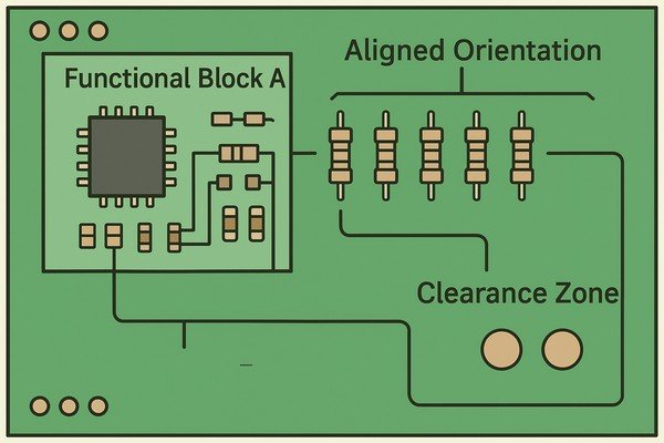
Good placement follows three core rules: group related components into functional blocks, orient similar parts in the same direction for assembly, and maintain proper clearances between components and to the board edge for manufacturability and electrical isolation.
My Golden Rules for Clean Layouts
These aren't just suggestions; they are rules I've learned to live by to avoid production issues and late-night debugging sessions. A clean, organized layout is a reliable layout.
Rule 1: Orientation for Manufacturability
Automated assembly machines work best with consistency. I always orient similar components, especially polarized ones like diodes and electrolytic capacitors, in the same direction. For ICs, I ensure Pin 1 is always in the same relative position (e.g., top-left). This simple discipline dramatically reduces the chance of assembly errors and makes visual inspection far easier.
Rule 2: Respecting Clearances
Components need breathing room. Cramming them together causes problems during assembly (pick-and-place nozzle collisions) and rework (no room for a soldering iron). I follow IPC standards as a baseline and confirm with the specific assembly house.
Rule 3: Logical Signal Flow
Arrange components to mirror the signal path on the schematic. If a signal comes from a connector, goes to a filter, then an amplifier, and finally an ADC, the physical layout should follow that exact sequence. This naturally results in shorter, more direct traces.
| Clearance Type | Guideline Source | Typical Value (Producibility Level B) | Reason |
|---|---|---|---|
| Component-to-Component | IPC-2221A | 0.5 mm (20 mils) | Prevents solder bridging, allows for rework access. |
| Component-to-Edge (routed) | IPC-2221A | 3.0 mm (120 mils) | Avoids damage during depanelization and handling. |
| Component-to-Mounting Hole | General Practice | 2.5 mm (100 mils) | Prevents shorts from fasteners and mechanical stress. |
What Common Placement Mistakes Affect Board Functionality?
Ever designed a board that looked perfect but failed on the test bench? Often, the root cause isn't a bad schematic but a subtle placement mistake that compromises electrical performance.
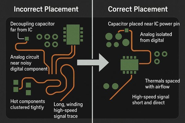
Common mistakes include placing decoupling capacitors too far from IC power pins, locating sensitive analog circuits near noisy digital or power components, ignoring thermal considerations by clustering hot parts, and creating long, meandering high-speed signal paths.
Avoiding Costly Placement Traps
I've spent countless hours troubleshooting boards where a simple placement choice was the culprit. These mistakes are easy to make but can be fatal to the design's functionality. Learning to spot them during the layout phase is a crucial skill.
The Decoupling Capacitor Disaster
This is the most common error. A decoupling capacitor1’s job is to provide a low-inductance path to ground for high-frequency noise. Placing it even 10mm away from the IC's power pin, or on the opposite side of the board, adds enough inductance to make it ineffective. It must be placed as close as physically possible to the pin it is serving.
Crosstalk from Poor Grouping
Noise is contagious. Placing a high-frequency switching power supply next to a low-noise amplifier is guaranteed to cause problems. The switching noise will electromagnetically couple into the sensitive analog traces, corrupting your signal. This is why strict functional grouping is non-negotiable.
High-Speed Signal Sabotage
In high-speed designs, traces are transmission lines. A long, winding path between a CPU and its memory creates timing problems and signal reflections. The components must be placed close enough to ensure the routed length meets timing constraints.
| Common Mistake | Consequence | Corrective Placement Action |
|---|---|---|
| Distant Decoupling Capacitor | High-frequency noise on power rails; IC instability. | Place capacitor < 2mm from the IC power pin, on the same layer. |
| Mixing Noisy & Sensitive Circuits | Digital noise couples into analog signals, reducing SNR. | Physically separate functional blocks (power, digital, analog). |
| Clustering Hot Components | Creates thermal hotspots, reducing component lifespan. | Distribute heat-generating components across the board. |
| Long High-Speed Traces | Signal reflections, timing errors, EMI radiation. | Place related high-speed components close together for short paths. |
What Is Functional Grouping for Component Placement?
Looking at a dense schematic can feel overwhelming. How do you translate that web of connections into a clean, organized layout? The secret is to not think about individual components, but about systems.
Functional grouping, also known as floorplanning, is the practice of partitioning the PCB layout into distinct sections based on the circuit's function. This means placing all components related to the power supply in one area, analog signals in another, and digital logic elsewhere.
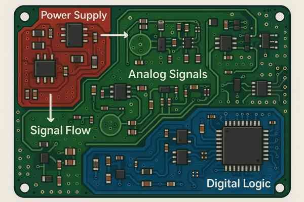
The 'City Planning' Approach to PCB Layout
I never start a complex layout without a floorplan. I treat the PCB like a city map: you need designated zones for industrial (power supply), residential (sensitive analog), and commercial (digital logic) areas to prevent chaos. This approach simplifies routing and makes the board electrically robust.
Identifying Your Functional Blocks
The first step is to analyze the schematic and identify the key systems. I literally draw boxes around these sections on the schematic printout. This creates a clear visual guide for the layout. For example, everything related to the 3.3V switch-mode power supply—the controller IC, inductor, MOSFETs, and filter caps—is one block.
Managing the Borders
Once the zones are defined on the PCB, the goal is to keep signals within their designated blocks as much as possible. When a signal must cross a border (e.g., an analog signal entering an ADC in the digital block), this interface becomes a critical point. I place the ADC right at the boundary to keep the analog trace out of the noisy digital area.
| Functional Block | Primary Placement Goal | Example Components |
|---|---|---|
| Power Supply | Minimize noise radiation, ensure thermal dissipation. | SMPS controllers, inductors, bulk capacitors. |
| Sensitive Analog | Isolate from all noise sources, ensure clean ground. | Op-amps, ADCs, sensors, audio circuits. |
| High-Speed Digital | Minimize trace lengths, control impedance. | CPU, FPGA, DDR memory, high-speed transceivers. |
| RF / Wireless | Isolate from digital noise, manage impedance for antenna. | Transceiver ICs, matching networks, filters. |
How Should Component Placement Be Used to Optimize Signal Path Integrity?
You want your signals to arrive at their destination clean and on time. Routing is important, but a signal's journey is determined long before you draw the first trace. Placement sets the stage for success or failure.
To optimize signal path integrity, place components sequentially to follow the schematic's signal flow, ensuring the path is as short and direct as possible. For high-speed signals, keep components close together to minimize trace length, and place them over a continuous ground plane to ensure a clean return path.
Designing for Pristine Signal Integrity from the Start
Signal integrity2 (SI) isn't black magic; it's physics. Good SI is achieved by controlling the electromagnetic fields that guide the signal. Your first and most powerful tool for controlling these fields is component placement.
The Shortest Path is the Best Path
Every millimeter of PCB trace adds inductance and capacitance, which can distort a signal. For high-speed signals, this is critical. I always place the driver and receiver components as close as possible to allow for the most direct route. A short path minimizes delay, reduces the chance of reflections, and makes the trace less of an effective antenna for radiating EMI.
The Critical Return Path
A signal requires a return path for its current, which ideally flows through the solid ground plane directly beneath the trace. When placing components, I visualize this return path. If I place two connected components where there's a split or cutout in the ground plane between them, the return current has to make a huge detour. This creates a large current loop, a major source of EMI and signal degradation.
| SI Checklist for Placement | Goal | Action During Placement |
|---|---|---|
| Minimize Trace Length | Reduce delay, reflections, and loss. | Place connected components as close together as possible. |
| Ensure Return Path | Provide a low-inductance return loop. | Place components over a continuous, unbroken reference plane. |
| Place Termination | Match impedance and absorb reflections. | Place series resistors at the driver; parallel resistors at the receiver. |
| Align Differential Pairs | Maintain signal balance and noise immunity. | Position components to allow for parallel, length-matched routing. |
Conclusion
Proper component placement is more than just fitting parts on a board; it's the strategic foundation of a successful electronic design, directly impacting performance, manufacturability, and reliability. Start smart.


