
You’ve spent weeks perfecting a complex PCB design, but the job isn’t over. One small ambiguity in your assembly instructions can cause a contract manufacturer to halt production, costing you thousands in NRE charges and a week of delays. Imagine getting that dreaded email: "Production on hold. Please clarify orientation for U5." The SMT line is idle, the clock is ticking on your launch date, and the problem could have been prevented with a clearer drawing. A great assembly drawing is your insurance policy against this.
A PCB assembly drawing is a technical document that shows exactly where and how every component, from ICs to screws, is placed on a bare printed circuit board. It’s the primary instruction manual for the person or machine assembling the final product.

Getting your board assembled correctly is non-negotiable. It’s the difference between a working product and an expensive paperweight. This drawing is the bridge between your design file and the physical, populated board. It removes ambiguity and ensures your contract manufacturer understands every single detail of your assembly requirements, from component orientation to the specific type of solder to be used. Let’s break down what makes a great assembly drawing.
What is the Difference Between PCB Fabrication and Assembly Drawings?
Ever felt the frustration of a supplier asking for information that should have been clear? This often happens when fabrication and assembly details get mixed up. They serve two different vendors and purposes.
An assembly drawing tells the assembler where to put the components. A fabrication drawing, on the other hand, tells the board house how to build the bare, unpopulated PCB itself. Mixing them up causes confusion and delays.

Streamlining the Supply Chain with Clear Documentation
I always think of this as two completely separate supply chains that converge at the end. The fabrication drawing goes to the PCB shop that only deals with laminates, copper, and drill bits. The assembly drawing goes to the contract manufacturer (CM). I once saw a junior engineer combine them. The board house, confused by the component outlines, quoted an extra $2,000 to manually "clean" the files. The assembler, missing the stack-up info, almost built the board with the wrong impedance profile. Separating them isn’t just neat—it’s financially prudent and prevents miscommunication that can derail a project.
Why Two Separate Documents Are Better
Keeping these documents distinct streamlines communication and assigns clear responsibility. Each document is tailored to a specific stage and a specific audience in the manufacturing process.
| Document | Primary Audience | Key Question it Answers | Potential Consequence of Merging |
|---|---|---|---|
| Fabrication Drawing | Bare Board Manufacturer | "How do I build the physical board structure?" | The assembler receives irrelevant details like drill tolerances and copper weights, causing confusion. |
| Assembly Drawing | Electronics Assembler (CM) | "Where do all the components go on this board?" | The board house is confused by component-level details like reference designators and polarity. |
What Information Does a PCB Assembly Drawing Contain?
Wondering if you’ve included enough detail in your drawing? A missing piece of information can halt an entire production run while the assembler waits for your answer. The goal is to leave no room for guessing.
A complete assembly drawing contains graphical views of the board with component outlines, reference designators, polarity marks, and any mechanical parts. It’s a visual map linking the logical design (schematic) to the physical product.

Anticipating Confusion and Adding Clarity
A good drawing is comprehensive. It must allow an engineer who has never seen your project before to build it. For dense boards, I add more than just top and bottom views. For a BGA part, a simple outline is useless. I always include a "Detail View," scaled up 5x, that explicitly shows the A1 corner marker and how it aligns with the silkscreen. For a press-fit connector that requires 200N of force, I add a callout directly on the drawing specifying this, so the assembly tech doesn’t have to hunt for it in a separate document. You have to anticipate confusion and provide proactive clarity.
Essential vs. Recommended Information
While some information is mandatory, adding recommended details can prevent costly assumptions on complex boards.
| Information Type | Details | Why It’s Important |
|---|---|---|
| Essential (Must Have) | Board views (Top/Bottom), Ref Des, Polarity Marks, Component Outlines, BOM Revision link. | Forms the absolute minimum instruction set. Without this, the board cannot be assembled. |
| Recommended (Good to Have) | Isometric Views, Detail Views, Mechanical Hardware locations (screws, etc.), Keep-out Areas. | Provides clarity for 3D clearance, highlights tricky areas, and prevents mechanical interference. |
| Conditional | Conformal coating masks, specific torque values for hardware, press-fit component instructions. | Necessary for high-reliability products or those with special mechanical requirements. |
Why is a Bill of Materials (BOM) Crucial for Assembly Drawings?
Have you ever had an assembler use the wrong part? An assembly drawing tells you where a component goes, but it doesn’t specify what that component is. That’s the job of the Bill of Materials.
The BOM is a detailed list of every single component to be mounted on the board. It links the reference designator on the drawing (e.g., "R1") to a specific manufacturer part number (MPN), ensuring the correct part is sourced and placed.

The Unbreakable Link Between Drawing and BOM
I learned this the hard way on an early project where the drawing was updated, but the BOM wasn’t. The assembler built 50 prototypes using an older capacitor value. It cost us a week and thousands of dollars. Now, my rule is rigid: the CM receives a single zip file named [ProjectName]_[Rev]_[Date].zip. Inside, the files are named [ProjectName]_[Rev]_Assembly.pdf and [ProjectName]_[Rev]_BOM.xlsx. The revision in the filename must match the revision inside the documents. This level of rigor seems obsessive until it saves you from a $10,000 rework.
The Anatomy of a High-Quality BOM
A detailed BOM prevents ambiguity in component sourcing and placement.
| BOM Field | Example | Purpose / Why it’s Critical |
|---|---|---|
| Reference Designator1 | C5, C8, C12 |
Links the physical location on the drawing to the part list. |
| Manufacturer Part Number (MPN)2 | CC0603KRX7R9BB104 |
The exact, unambiguous part to order. Prevents sourcing errors. |
| Quantity | 3 |
Ensures the correct number of parts are ordered for the board. |
| Description | CAP CER 0.1UF 50V X7R 10% 0603 |
Human-readable check to quickly spot obvious errors (e.g., wrong value). |
| Alternate MPN | CL10B104KB8NNNC |
Pre-approved substitute that prevents production delays during part shortages. |
How is Component Polarity and Orientation Shown on an Assembly Drawing?
Putting a polarized capacitor in backward can cause it to fail, sometimes spectacularly. Incorrectly orienting an IC can damage the chip and the board. These are simple mistakes born from unclear drawings.
Component polarity and orientation are shown using standardized visual cues. This includes a ‘+’ symbol for tantalum capacitors, a chevron or dot for Pin 1 on an IC, and diode symbols that match the physical part’s marking.

Eliminating Ambiguity in Component Placement
Ambiguity is the enemy of manufacturing. For asymmetrical connectors, I add a small, unique shape like a triangle or star to the assembly layer at Pin 1. A simple dot can be confused with a via. A unique shape is impossible to misinterpret and helps the AOI system learn the correct orientation faster. When designing a footprint, I make sure the silkscreen has a clear Pin 1 marker, but since it can be obscured, the assembly drawing is the final authority. A clear mark takes seconds to add but can save days of debugging.
A Visual Glossary of Polarity Markings
Using standard, unambiguous markings is essential for correct assembly.
| Component Type | Standard Marking Convention | Common Mistake to Avoid |
|---|---|---|
| Integrated Circuit (IC) | A dot, number ‘1’, or beveled corner on the outline next to Pin 1. | Relying only on silkscreen which can be hidden under the part. The drawing must be clear. |
| Diode / LED | A line indicating the cathode bar, or the full schematic symbol outline. | Using a symmetric circle for a diode marking, which is ambiguous. |
| Polarized Capacitor | A + symbol on the drawing to mark the positive terminal. |
Forgetting the + mark, forcing the assembler to guess based on pad shape. |
| Connector | A number ‘1’ or a unique symbol (e.g., triangle) to explicitly identify the first pin. | Assuming the assembler knows the standard pinout for a generic connector type. |
What Are Assembly Notes and What Do They Specify?
Have you ever needed to communicate a special requirement that isn’t graphical? This is what the assembly notes are for. They are the text-based instructions that cover everything else.
Assembly notes are a list of instructions on the drawing that specify processes, standards, and other non-graphical requirements. They cover everything from the solder type to be used to how the board should be cleaned and inspected after assembly.

Communicating Process Requirements Beyond the Graphics
I treat notes as my direct line to the process engineer. When working with global CMs, specific notes are critical. Vague instructions like "clean well" can be interpreted differently. A specific note like "CLEAN PER IPC-A-6103 SEC 10.6.3, AQUEOUS WITH DI WATER RINSE" provides a universal, measurable standard. For aerospace projects, I always add a note specifying if ITAR (International Traffic in Arms Regulations) apply. For medical devices, I’ll specify torque values for hardware (e.g., "TORQUE M3 SCREWS TO 0.5 Nm ±5%"). These notes are a binding part of the manufacturing instructions.
Structuring Your Assembly Notes
Organizing notes by category makes them easier for your CM to process and follow.
| Note Category | Example Phrasing | Reasoning / Impact |
|---|---|---|
| Workmanship | "ALL WORKMANSHIP SHALL CONFORM TO IPC-A-610, CLASS 2." | Sets the overall quality standard for the entire assembly. |
| Materials | "SOLDER ALL COMPONENTS USING SAC305 LEAD-FREE SOLDER ALLOY." | Specifies the exact materials to be used, critical for reliability and compliance (e.g., RoHS). |
| Process | "APPLY CONFORMAL COATING (MATERIAL XYZ) TO TOP SIDE." | Defines specific manufacturing steps that are not part of standard assembly. |
| Compliance | "THIS ASSEMBLY MUST BE ROHS COMPLIANT. ITAR RESTRICTIONS APPLY." | Communicates critical legal and regulatory requirements. |
Are There Standards for Creating PCB Assembly Drawings?
How do you ensure your drawing will be universally understood by any manufacturer, anywhere in the world? You use industry standards. They provide a common language for electronics manufacturing.
Yes, the primary standard is IPC-D-325, which provides documentation requirements for printed boards. More importantly, the drawing will reference workmanship standards like IPC-A-610 (Acceptability of Electronic Assemblies) and soldering standards like J-STD-001.

Using Industry Standards as a Communication Shortcut
Relying on standards saves my projects countless times. Instead of describing a good solder joint, I write, "SOLDER PER J-STD-0014, CLASS 2." This instantly communicates a volume of requirements. It’s also important to note that specifying a higher class is not free. A CM will charge more for Class 3 assembly because it requires more rigorous inspection and slower process speeds. I only specify Class 3 when the application (life support, mission-critical aerospace) absolutely demands it. For most commercial products, Class 2 is the optimal balance of reliability and cost.
Referencing the correct standard on your drawing eliminates ambiguity and sets clear quality expectations.
| Standard | Full Title | What It Governs in Practice |
|---|---|---|
| IPC-A-610 | Acceptability of Electronic Assemblies | The "visual dictionary" for quality. Defines target conditions and defects for everything from soldering to component mounting. |
| J-STD-001 | Requirements for Soldered Electrical and Electronic Assemblies | The "how-to" guide for soldering. Specifies the materials, methods, and verification criteria for creating reliable solder joints. |
| IPC-D-3255 | Documentation Requirements for Printed Boards | The foundational standard that outlines the general requirements for the set of documents needed to describe a PCB. |
What Common Errors Occur in PCB Assembly Drawings?
What are the simple mistakes that can derail a project? After reviewing hundreds of design packages, I see the same preventable errors pop up again and again. They are almost always related to ambiguity or outdated information.
The most common errors are mismatched BOM revisions, unclear polarity markings, incorrect component footprints, missing mechanical parts, and ambiguous assembly notes. These issues create confusion, force production stops, and lead to costly rework.

Learning from Costly Mistakes: A Proactive Approach
I once had to scrap an entire run of 200 boards because the assembly drawing showed an old version of a connector. The BOM was correct, but the assembler followed the drawing’s physical outline. The single most effective habit I’ve developed is a peer review of the entire design package—schematic, layout, BOM, and drawings—before releasing it. A fresh set of eyes almost always catches a misaligned reference designator or a note that references a non-existent part. It’s a small time investment that can prevent catastrophic downstream costs.
A Framework for Error Prevention
A systematic check before release can catch over 90% of common documentation errors.
| Error Category | Specific Mistake | Prevention Tactic |
|---|---|---|
| Version Control | Drawing references BOM Rev A, but you send BOM Rev B. | Create a single release package (e.g., a .zip file) with all matching documents. Name the zip with the project and revision. |
| Component Ambiguity | A diode’s polarity is marked with a simple circle. | Use markings that are impossible to misinterpret, like a full diode symbol overlay. |
| Mechanical Mismatch | Forgetting to include a keep-out area under a large heat sink. | Import a 3D STEP model of the mechanical enclosure into your ECAD tool to check for interferences before creating the drawing. |
| Note Inconsistency | A note specifies a process that contradicts another note. | Read every note out loud. This often reveals conflicting or unclear instructions. |
Where Can Examples of Good Assembly Drawings Be Found?
It’s hard to create a good drawing without ever seeing one. So where can you find professional-grade examples? Since most commercial designs are confidential, you have to look in the open-source world.
Good examples of assembly drawings can often be found in the documentation for open-source hardware projects and evaluation kits from major component manufacturers. Companies like Adafruit, SparkFun, and semiconductor giants like STMicroelectronics or Texas Instruments often provide full documentation.

Learning from the Pros: Deconstructing Open-Source Examples
When I’m mentoring junior engineers, I point them to the documentation for a product like the BeagleBone Black or official Raspberry Pi HATs. These companies know their designs will be scrutinized by thousands of engineers. Don’t just look at the PDF. Look for the "Output Job File" in Altium or the plot scripts in KiCad. This is the "recipe" they used to generate the drawing. Replicating their recipe is a great way to learn how to structure layers and notes for maximum clarity.
What to Look For: A Checklist
When evaluating an example drawing, check for these signs of quality and completeness.
| Attribute | What it Looks Like in Practice |
|---|---|
| Clarity | The drawing is easy to read. Reference designators don’t overlap with pads or other text. |
| Completeness | It has all the key elements: views, notes, a title block, and a BOM reference. |
| Revision Control | There is a clear title block with a revision history table showing changes, dates, and author. |
| Precision | Important details, like the location of a press-fit pin, are called out with a detail view and dimensions. |
What Software Is Used to Generate Assembly Drawings?
Are you supposed to draw these by hand? Of course not. Modern engineering relies on specialized software to automate the creation of these critical documents from your PCB layout data.
Assembly drawings are generated by the same Electronic Design Automation (EDA) software used to design the PCB itself. The most common tools are Altium Designer, Cadence Allegro, Siemens EDA (Mentor Graphics) PADS, and the open-source option, KiCad.

The Power of Integrated EDA Tools
The key is that the assembly drawing generator is an integrated feature of the layout tool. This ensures the drawing is directly linked to the design database. Beyond the design tools, a good engineer understands the tools their partners use. I always recommend my CMs use a quality Gerber/ODB++ viewer like Ucamco’s free Reference Gerber Viewer. It allows them to inspect layers independently, providing another layer of verification. The tool itself matters less than a deep understanding of what information must be conveyed.
Comparing Popular EDA Software for Documentation
Each software has a different approach to generating documentation.
| Software | Key Documentation Feature | Best For… |
|---|---|---|
| Altium Designer | Draftsman: A dedicated, integrated tool for creating polished drawing packages. | Engineers and teams who need to produce high-quality documentation efficiently. |
| KiCad | Plot Menu: A flexible system for exporting layers (to PDF, SVG, etc.) for manual composition. | Hobbyists, startups, and professionals looking for a powerful, no-cost solution. |
| Cadence Allegro | Design Publisher: A robust documentation system designed for complex, high-speed boards. | Large enterprise environments where integration with other simulation and management tools is key. |
How Are Assembly Drawings Created From Design Software Like Altium or KiCad?
Okay, so you have the software. What are the actual steps to generate the drawing? It’s a process of selecting and configuring the right layers and views from your completed PCB layout.
In tools like Altium or KiCad, you create an assembly drawing by generating views of your board and overlaying specific design layers. This typically includes assembly layers (with component outlines), silkscreen layers, pad layers, and the board outline.
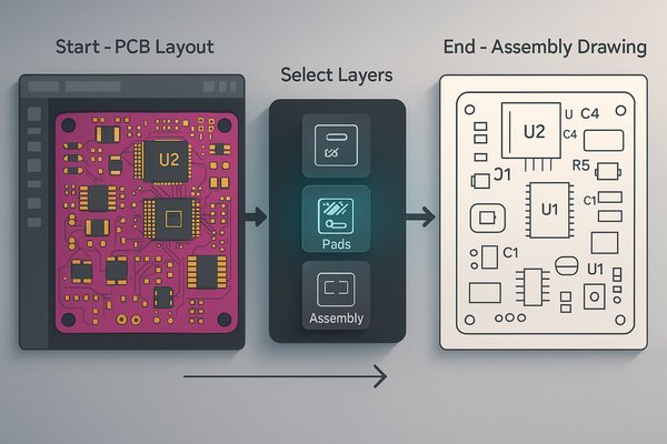
The Practical Steps of Generating a Drawing
The process feels like building a map from different transparencies. In any software, the key is to use dedicated fabrication or assembly layers (Fab, Docu, Mech) during layout to place information that you don’t want on the final silkscreen but need on the assembly drawing. This keeps your design source clean while producing comprehensive documentation. For example, I place detailed courtyard and polarity markers on a mechanical layer that is only visible in the assembly drawing, not on the board’s silkscreen.
Layer Selection for Assembly Drawings
Choosing the right layers is key to a clear and useful drawing.
| Purpose | Layer Name in Altium | Layer Name in KiCad | Pro Tip |
|---|---|---|---|
| Component Outlines/Polarity | Mechanical Layer or tDocu |
F.Fab (Front Fab) / B.Fab |
Use a thicker line weight for outlines to make them stand out. |
| Reference Designators | Top Overlay / Bottom Overlay |
F.SilkS (Front Silkscreen) |
Ensure text is not placed over vias or pads where it will be unreadable. |
| Board Outline | Keep-Out Layer or Mechanical Layer |
Edge.Cuts |
Include board dimensions from the outline for a quick sanity check. |
| Pads / Vias | Top Layer / Bottom Layer |
F.Cu (Front Copper) |
Show only pads, not routing, to avoid cluttering the drawing. |
What Are a Contract Manufacturer’s Requirements for Assembly Drawings?
You’ve created a beautiful drawing. But is it what your manufacturing partner actually needs to build your board without calling you every five minutes? Understanding their perspective is key to a smooth process.
A contract manufacturer (CM) requires an assembly drawing that is clear, unambiguous, and complete. It must work in concert with a matching BOM and centroid (pick-and-place) file to enable both automated and manual assembly processes.

Thinking Like Your Manufacturer: The Key to a Smooth Handoff
From my current role, I spend a lot of time talking to CMs. Their biggest request is simple: consistency across the entire design package. Before I send a package to a new CM, I often run it through a third-party DFM (Design for Manufacturability6) tool. These tools often catch issues like solder mask slivers or acid traps that my internal DRC might miss. Sending a "clean" package that has been pre-vetted builds trust with your CM from day one and shows that you respect their process and time. It’s a small step that pays huge dividends in the relationship.
The "Perfect" Design Package for Your CM
Providing a complete and consistent set of of files is the best way to ensure a smooth manufacturing run.
| Deliverable File | Purpose | Pro Tip from a CM’s Perspective |
|---|---|---|
| Assembly Drawing (PDF) | The master human reference for all assembly, inspection, and rework. | Please make it readable. Don’t use tiny fonts or overlapping text. |
| Bill of Materials7 (XLSX) | The master list for sourcing parts. | Include approved alternate parts to avoid line-down situations. |
| Centroid File (CSV/TXT) | The machine file for programming the Pick and Place equipment. | Ensure the rotation for your components is correct (0, 90, 180, 270 degrees). |
| Gerber/Fabrication Files | To order the bare boards (often handled by the CM). | Include the fabrication drawing so they know the required board specs. |
How Do Assembly Drawings Support Automated Manufacturing?
How does a drawing—a document made for humans—help a robot place 10,000 components per hour? It serves as the essential reference and verification tool that supports the machine-readable data.
Assembly drawings support automated manufacturing by providing the human-readable master plan. While machines use centroid files for component placement and AOI systems use rendered images for inspection, the drawing is used by operators to set up, verify, and debug these automated processes.

The Human-Readable Guide for a Robotic Process
Think of the automated assembly line. While a PDF drawing is the human-facing standard, the industry is moving toward all-in-one data formats like IPC-25818. This single file contains everything: stack-up, drill data, component info, and netlist. It’s one "source of truth" for both machines and humans. I always generate an IPC-2581 file alongside my traditional package. It shows the CM that I’m aligned with modern best practices, but I still provide the PDF drawing because it remains the ultimate, universal source of truth on the factory floor for any manual intervention or quality check.
The Drawing’s Role in the Smart Factory
The assembly drawing is the critical link between automated processes and the humans who manage them.
| Automated Process | Machine-Readable Input | How the Assembly Drawing is Used by Humans |
|---|---|---|
| SMT Programming | Centroid (Pick and Place) File, IPC-2581 | The operator uses the drawing to visually verify the first article, ensuring the machine’s setup matches the design intent. |
| Automated Optical Inspection (AOI)9 | A "Golden Board" image derived from CAD data. | When the AOI flags a potential defect, a technician uses the drawing to determine if it’s a real failure or a false positive. |
| Manual Assembly / Rework | N/A | This process is entirely reliant on the assembly drawing for placing through-hole parts, press-fit connectors, or fixing misplaced components. |
Conclusion
An assembly drawing is more than just a formality. It is the single most important document for ensuring your design is manufactured exactly as you intended, protecting your project from costly delays.
-
Discover the significance of Reference Designators in linking components to their physical locations, enhancing clarity in designs. ↩
-
Learn how MPNs ensure accurate sourcing and prevent errors in your projects. This resource will deepen your understanding. ↩
-
Understanding IPC-A-610 is crucial for ensuring quality standards in manufacturing processes, especially in electronics. ↩
-
Explore this link to understand the significance of J-STD-001 in ensuring reliable solder joints and quality in electronic assemblies. ↩
-
Discover the essential requirements of IPC-D-325 for PCB documentation, crucial for maintaining clarity and quality in electronic design. ↩
-
Understanding DFM can significantly enhance your design process and improve collaboration with manufacturers. ↩
-
A well-structured BOM is crucial for efficient sourcing and production, ensuring no parts are overlooked. ↩
-
Explore this link to understand IPC-2581, a modern data format that enhances efficiency in manufacturing processes. ↩
-
Discover the significance of AOI in manufacturing and how it helps maintain product quality through visual inspections. ↩


