Struggling with inconsistent wireless performance on your new IoT device? Your PCB antenna might be the hidden source of signal loss, causing major headaches and project delays.
The main disadvantages of PCB antennas are lower efficiency and gain, high sensitivity to nearby components and dielectrics, a larger required board area, and complex tuning. They are easily detuned by enclosures, hands, or even component variations, leading to unreliable performance.
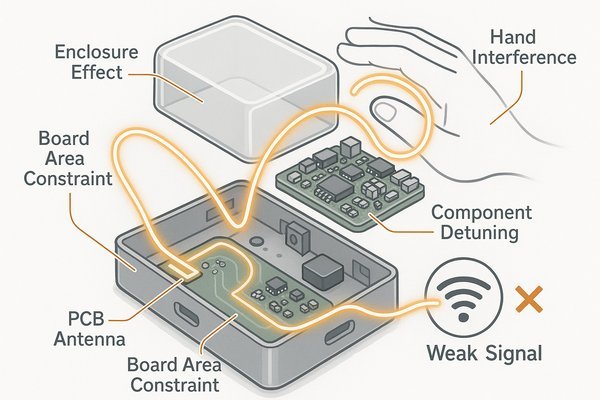
These drawbacks can be deal-breakers for high-performance applications. Before you rule them out, it's crucial to understand the full picture. The table below summarizes the core challenges, and then we'll explore each one in more detail.
| Drawback | Technical Reason | Practical Impact on Project |
|---|---|---|
| Lower Efficiency/Gain | High dielectric loss of FR-4 material; non-ideal geometry. | Reduced communication range; higher transmit power needed; unreliable connection. |
| High Sensitivity | Performance is coupled to nearby materials (plastic, metal, hands). | Unpredictable performance; requires testing in the final enclosure; risk of field failures. |
| Complex Tuning | Requires impedance matching using a VNA and manual component changes. | Increased NRE cost; requires specialized RF expertise and equipment; slows prototyping. |
| Larger Footprint | Antenna length is proportional to wavelength (λ). | Consumes valuable PCB real estate; can constrain industrial design and product size. |
A Closer Look at the Key Drawbacks
Understanding the "why" behind the disadvantages is critical for any engineer considering a PCB antenna. It’s not enough to know they are "less efficient"; you need to know why that efficiency is lost and how your design choices can make it worse.
Efficiency and Gain Limitations
A typical PCB antenna might have a radiation efficiency of only 30-60%, whereas a simple external dipole can exceed 80%. This loss happens because the standard FR-4 board material is not ideal for RF. FR-4 has a relatively high dielectric loss tangent (tan(δ)), typically between 0.015 and 0.025 at 2.4 GHz. This means a significant portion of the electrical energy is converted into heat within the PCB material itself instead of being radiated as a signal. In contrast, high-frequency laminates like those from Rogers have loss tangents below 0.004, but they are far more expensive. This efficiency loss directly impacts gain, meaning a PCB antenna needs a stronger signal from the transceiver to achieve the same range as a more efficient antenna.
Extreme Sensitivity to the Environment (Detuning)
A PCB antenna is not just the copper trace; it's a system that includes the board material, the ground plane, and everything around it. I once saw a project where the antenna performed perfectly on the lab bench but failed in the field. The cause? The final plastic enclosure used a flame-retardant additive that was more RF-absorbent than we had modeled. This shifted the antenna's center frequency by over 100 MHz, destroying the link budget. This effect, called detuning, also happens from the "hand effect"—a user holding the device can detune the antenna and block the signal. This sensitivity requires careful modeling and testing of the antenna inside its final, assembled product, not just on a bare board.
The Complex Challenge of Tuning
Every PCB antenna requires a custom matching network (usually a 3-component Pi-network) to match its impedance to the standard 50 Ω of the radio. This isn't a simple "set and forget" process. It's an iterative task requiring a Vector Network Analyzer (VNA). You must test the antenna, analyze the result on a Smith Chart, calculate new capacitor and inductor values, replace the tiny 0402 or 0201 components, and test again. This process must be repeated until the Voltage Standing Wave Ratio (VSWR) is acceptable—ideally below 1.5:1. Doing this properly requires expensive equipment and several hours of a skilled RF engineer's time for each design iteration.
What Are The Advantages of PCB Antennas?
Trying to cut costs and simplify your Bill of Materials (BOM)? Integrating an antenna can seem complex, but what if it cost virtually nothing and was already part of your board?
The key advantages of PCB antennas are an extremely low cost, zero assembly labor, and high reliability since they are immune to shock and vibration. They are easily integrated into the existing PCB layout, simplifying the supply chain and manufacturing process.
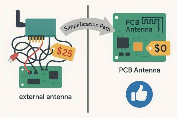
Why Cost and Reliability Make PCB Antennas a Go-To Choice
The benefits of a PCB antenna go far beyond the initial component cost. As a hardware engineer who has managed large-scale product platforms like the Honeywell Tuxedo Keypad, I've seen firsthand how these advantages translate into real-world success, especially in high-volume production.
True Cost Savings
The most obvious advantage is cost. A PCB antenna isn't a separate component. Its cost is the price of the copper and FR-4 it occupies. Let's quantify this. For a 1 million unit production run, choosing a PCB antenna over a $0.15 chip antenna saves $150,000 on components alone. Add another $0.05 per unit for assembly (pick-and-place and soldering), and you save an additional $50,000. That's $200,000 in direct savings, a number that gets any project manager's attention.
Enhanced Reliability and Simplified Manufacturing
Since the antenna is etched directly onto the board, it is not a separate physical part. This provides several manufacturing and reliability benefits, as shown in the table below.
| Advantage | Benefit |
|---|---|
| No Assembly Step | Reduces manufacturing cost and time. |
| No Solder Joints | Eliminates a common point of mechanical failure. |
| High Shock/Vibration Resistance | Increases product robustness in harsh environments. |
| Simplified BOM & Supply Chain | Reduces inventory management and sourcing complexity. |
This inherent robustness is critical in industrial or consumer devices that are subject to physical stress.
Full Design Control
When I design a PCB antenna, I have complete control in my EDA tool. I can integrate it with advanced ground plane strategies, such as using stitched vias around the antenna keep-out area to prevent surface currents and improve isolation. I can also shape the ground plane itself to act as a counterpoise, effectively making it part of the radiating structure. This level of system-level optimization is impossible with a fixed, off-the-shelf component.
How Do PCB Antennas Work?
Ever wondered how a simple copper trace can send and receive signals across the room? It seems like magic, but it is pure physics that can cause major design headaches when misunderstood.
A PCB antenna works by acting as a resonant structure. When an RF signal at a specific frequency is fed to the trace, it creates standing waves of current and voltage. This oscillating electric and magnetic field radiates away from the PCB as an electromagnetic wave.
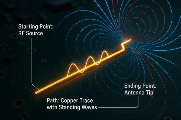
How a Simple Trace Becomes a Complex RF System
At its core, an antenna is a transducer. It converts guided electrical signals from a transmission line into electromagnetic waves propagating in free space, and vice versa. Understanding how a simple PCB trace achieves this is fundamental for any RF hardware designer.
The Principle of Resonance
Any conductor carrying an alternating current (AC) will radiate some energy. An antenna is a structure specifically designed to make this radiation process efficient at a particular frequency. The physical dimensions of the antenna are directly related to the wavelength (λ) of the signal. For example, a basic quarter-wave monopole antenna for 2.4 GHz Wi-Fi has a physical length related to λ/4. For 2.4 GHz, the full wavelength in free space is about 12.5 cm, so a quarter-wave element is approximately 3.1 cm. The trace on the PCB acts as this resonant element.
The Importance of Impedance Matching
For maximum power transfer from the radio transceiver to the antenna, their impedances must match. The industry standard is 50 Ω. A poor match creates a high Voltage Standing Wave Ratio (VSWR)1, which means power is reflected back toward the transceiver. The impact of a poor match is not trivial, as shown in the table below.
| VSWR | Reflected Power (%) | Transmitted Power (%) | Performance Quality |
|---|---|---|---|
| 1:1 | 0% | 100% | Ideal / Perfect Match |
| 1.5:1 | 4% | 96% | Excellent |
| 2:1 | 11.1% | 88.9% | Good / Acceptable |
| 3:1 | 25% | 75% | Poor / Significant Loss |
| 5:1 | 44.4% | 55.6% | Bad / Unacceptable |
A VSWR above 2:1 not only reduces the radiated signal but can also damage the radio's power amplifier over time.
The Critical Role of the Ground Plane
A common mistake is to design the antenna trace in isolation. The ground plane is an active part of the antenna system. It acts as the "other half" of the antenna, shaping the radiation pattern and influencing the impedance. The size of the ground plane and the clearance area around the antenna trace are critical. According to antenna design guidelines, such as those in the Texas Instruments Antenna Design and Selection Guide (SWRU120B), the ground plane clearance is paramount for achieving the designed performance. A clearance of at least 3H, where H is the thickness of the substrate, is a bare minimum starting point.
What Are The Main Types of PCB Antennas?
Choosing an antenna type from a sea of options feels overwhelming. Picking the wrong one can kill your product's performance, forcing a costly and time-consuming redesign late in the development cycle.
The most common PCB antenna types are the Inverted-F Antenna (IFA), popular for its compact size in IoT devices; the Meander Line Antenna (MLA), used to save space but with lower efficiency; and the Patch Antenna, which is effective at higher frequencies like GPS.

A Practical Guide to Common Antenna Geometries
The geometry of the PCB trace defines the antenna's characteristics. I choose the type based on the project's constraints: available space, required frequency, and performance targets.
Inverted-F Antenna (IFA)2
The IFA is the workhorse for Wi-Fi and Bluetooth. It's essentially a folded quarter-wave monopole, which gives it a compact footprint. Critically, it produces a relatively omnidirectional radiation pattern, meaning it transmits and receives well in most directions along its horizontal plane. This is ideal for mobile devices that change orientation frequently.
Meander Line Antenna (MLA)3
When board space is the absolute top priority, designers use the MLA. This shortens the antenna's footprint by folding a long trace back and forth. This meandering can reduce the required linear space by over 50%, but it comes at the cost of a 3-6 dB drop in gain compared to a proper monopole. The sharp bends and coupled segments create parasitic capacitance and field cancellation that severely hurts efficiency.
Patch Antenna4
For higher frequencies like GPS (1.575 GHz) or 5G, a microstrip patch antenna is a good choice. It consists of a rectangular "patch" of copper over a ground plane. They are inherently directional, radiating most of their energy in the direction perpendicular to the patch surface. This is perfect for a GPS unit in a car dashboard, which needs to face the sky, but poor for a handheld device that moves around.
| Antenna Type | Typical Use Case | Size | Efficiency | Bandwidth |
|---|---|---|---|---|
| Inverted-F (IFA) | Wi-Fi, Bluetooth, Zigbee | Compact | Moderate (30-60%) | Narrow to Moderate |
| Meander Line (MLA) | Space-constrained IoT | Very Compact | Low (10-40%) | Very Narrow |
| Patch Antenna | GPS, 5G (mmWave) | Medium | High (50-80%) | Narrow |
| Loop Antenna | NFC (13.56 MHz) | Large | N/A (Magnetic Field) | Very Narrow |
How Do PCB and Chip Antennas Compare?
Stuck deciding between designing your own PCB antenna or buying a pre-made chip antenna? This critical choice impacts your project's cost, performance, and ultimate time-to-market.
PCB antennas are cheaper but larger and require significant custom design and tuning effort. Chip antennas offer a smaller footprint and more predictable performance out-of-the-box, but at a higher component cost, and they are still sensitive to layout.
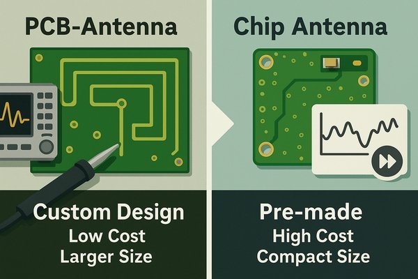
Making the Call: PCB Trace vs. Chip Antenna
Choosing between a PCB trace and a chip antenna5 is a classic engineering trade-off. I've used both extensively, and the decision always comes down to balancing NRE cost6, unit cost, performance, and schedule risk.
Design Effort and NRE
A PCB antenna requires a significant upfront investment in engineering time (NRE). This involves electromagnetic simulation, multiple prototype board spins, and hours of VNA testing. A chip antenna manufacturer has already done this work. My job is to follow their layout guidelines precisely. This lowers design risk, which is critical for tight schedules.
Predictability and Performance
Chip antennas offer predictable performance. The datasheet provides key metrics, giving you a solid baseline. A PCB antenna's performance is unknown until it's built and tested inside the final product. While a well-designed PCB antenna can perform very well, its performance is unique to that specific PCB stack-up and enclosure.
Time-to-Market Considerations
This is often the deciding factor. On the Honeywell Tuxedo Keypad project, using a custom PCB antenna across the platform saved significant cost, but the initial validation took months. For a startup's first product, the predictability of a chip antenna can get you to market 2-3 months faster. That speed can be worth far more than the per-unit cost savings.
| Feature | PCB Antenna | Chip Antenna |
|---|---|---|
| Unit Cost | Essentially $0 | $0.15 to $0.50 |
| NRE / Design Cost | High (simulation, multiple prototypes) | Low (follow datasheet layout guide) |
| Board Space | Larger, dictates board outline | Very small (e.g., 3.2mm x 1.6mm) |
| Performance | Variable, highly design-dependent | More predictable, good efficiency for its size |
| Tuning | Always required, can be complex | Always required, but often a simpler process |
| Best For | Cost-sensitive, high-volume products | Space-constrained, time-sensitive projects |
How Do PCB Antennas Compare to External Antennas?
Your device needs the best possible wireless range. But a bulky external antenna can ruin the product's sleek design and robust feel, creating a difficult trade-off between performance and aesthetics.
External antennas almost always offer superior performance (higher gain and efficiency) compared to PCB antennas. However, they come at a much higher cost, increase product size, and introduce mechanical failure points via connectors and cables. PCB antennas prioritize integration over raw performance.
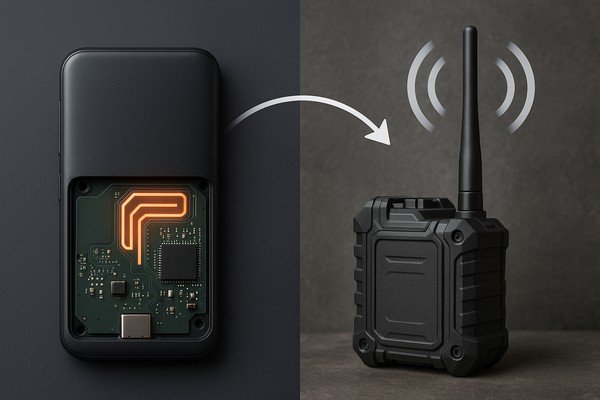
The Ultimate Trade-Off: Integration vs. Raw Performance
The decision between an integrated PCB antenna and an external antenna defines the product's capabilities and physical form factor. While a PCB antenna is part of the electronics, an external antenna is part of the product's industrial design.
The Performance Gap
The performance difference is significant. A 6 dB improvement in link budget, which is a realistic difference between a poor PCB antenna and a good external one, can quadruple the reliable communication range. For a device operating at the edge of its range, this is the difference between working and not working. This performance boost from an external antenna is often non-negotiable for mission-critical or long-range applications.
Cost, Reliability, and Mechanical Design
An external antenna solution is far more expensive, adding $2 to $7 to the BOM cost. It also introduces mechanical reliability risks. Connectors can loosen, and the external antenna itself can be damaged. Furthermore, for products requiring an Ingress Protection (IP) rating7 for water and dust resistance, like IP67, an external antenna complicates things immensely. It requires a specially sealed connector to be used, which adds further cost and assembly complexity. An internal PCB antenna keeps the enclosure fully sealed by default, simplifying rugged product design.
| Feature | PCB Antenna | External Antenna |
|---|---|---|
| Performance (Gain/Efficiency) | Low to Moderate (-5 to 2 dBi, 30-60%) | High (2 to 9 dBi, 70-95%) |
| Cost | Very Low (~$0) | High ($2 - $7 per unit) |
| Size / Aesthetics | Invisible, zero added volume | Adds external bulk, can be unsightly |
| Reliability | Very High (integrated into PCB) | Lower (connectors, cables, physical damage are risks) |
| Design Flexibility | Limited by product enclosure and PCB layout | Can be placed optimally for best signal reception |
| Certification (FCC/CE) | Part of the main board certification process | System must be certified with the specific antenna used |
Conclusion
PCB antennas offer huge cost and integration benefits. However, this comes at the price of lower performance and requires significant engineering expertise to design, tune, and implement correctly.
-
Understanding VSWR is crucial for optimizing RF systems and ensuring efficient power transfer. Explore this link for in-depth insights. ↩
-
Explore the benefits of IFA antennas, especially for mobile devices, to understand their omnidirectional capabilities and compact design. ↩
-
Learn about the Meander Line Antenna's design and efficiency trade-offs, crucial for space-constrained applications. ↩
-
Discover how Patch Antennas are optimized for high-frequency applications like GPS and 5G, enhancing directional performance. ↩
-
Discover the advantages of chip antennas, including predictability and space efficiency, which can be crucial for your project timelines. ↩
-
Learn about the implications of NRE costs in electronics design, which can significantly affect your project's budget and timeline. ↩
-
Exploring IP ratings will clarify their importance in ensuring device durability and reliability in various environments. ↩


