 Skip to content
Your wireless device has terrible range, and you suspect the software. But what if the problem is hiding in your hardware? It's likely an impedance mismatch silently killing your signal.
Impedance matching is critical because it ensures maximum power transfer from the radio transceiver to the antenna. Without a proper match, typically to 50 \(\Omega\), power is reflected back, causing severe signal loss, reduced range, poor efficiency, and potential failure during regulatory certification testing like FCC/CE.
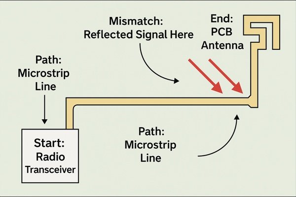
This might sound complex, but it's a fundamental concept in RF engineering. I've seen many projects get delayed because a simple mismatch rendered the entire wireless system useless. The good news is that once you understand the "why," the "how" becomes much clearer. Getting this right from the start saves countless hours of debugging and avoids costly board respins. Let's dive into the practical steps and best practices to ensure your antenna performs exactly as intended.
What are PCB antenna design best practices?
Designing a PCB antenna feels like black magic. A tiny layout error can ruin performance, forcing you to go back for an expensive and time-consuming board respin. Follow these proven practices.
Key best practices include strictly maintaining a 50-\(\Omega\) impedance for the feedline, creating a large and clear ground plane keep-out zone around the antenna, choosing appropriate PCB materials, and placing the antenna far from noisy components or metal enclosures for optimal radiation.
The Engineering Details
In my nearly 20 years of hardware design, I’ve learned that RF performance is won or lost in the layout details. It’s not about one single thing, but a combination of key elements. The 50-\(\Omega\) feedline is non-negotiable, but just as important is the ground plane it references. For many antenna types, like monopoles and PIFAs, the ground plane isn't just a signal return path; it's an active part of the antenna system, acting as the "counterpoise" or the other half of the radiator. A small or poorly designed ground plane will cripple performance. I also insist on including a pi-network footprint (a series element with two shunt elements) right at the antenna feed point on every design. Even with perfect calculations, manufacturing tolerances and enclosure effects will slightly alter the impedance. This network allows you to fine-tune the match with simple component changes, saving you from a board respin.
Here are some common antenna types you might implement on a PCB:
| Antenna Type | Common Application | Key Characteristic |
|---|---|---|
| Monopole (Trace) | Wi-Fi, Bluetooth, IoT | Simple \(\frac{\lambda}{4}\) trace. Requires a large ground plane as a counterpoise. |
| Inverted-F (PIFA)1 | Mobile Phones, GPS | Compact, folded monopole with a shorting pin. Balances size and performance. |
| Chip Antenna | Space-constrained devices | A tiny ceramic component. Requires careful layout per the datasheet. |
| Loop Antenna | NFC, RFID | Primarily magnetic field coupling. Less sensitive to detuning from hand effects. |
And here are the core practices I follow for all of them:
| Practice Area | Best Practice & Justification |
|---|---|
| Impedance Control2 | Design the feedline for 50 \(\Omega\). This is the industry standard for most RF chips and test equipment. Use an online or EDA tool's calculator. |
| Grounding | Provide a solid, unbroken ground plane under the feedline. For many antennas, the ground plane itself acts as the counterpoise. Ensure it's large enough for the operating frequency. |
| Matching Network | Always include a placeholder for a 3-element pi-network (e.g., C-L-C or L-C-L) for tuning. It's the cheapest insurance policy you can buy against a board respin. |
| Placement on PCB | Position the antenna at the edge or corner, far from other components, to maximize exposure. The ideal placement is often dictated by the antenna's radiation pattern and the product's use case. |
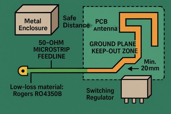
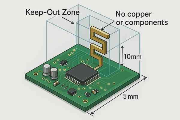
What is the keep-out zone for a PCB antenna?
Your antenna performance is poor, and you can't figure out why. Nearby ground planes or components could be detuning it, effectively blocking its signal. Define a strict keep-out zone to fix this.
A keep-out zone is a three-dimensional area around the antenna element where no copper (ground, traces, vias) or components should be placed. This prevents parasitic capacitance and detuning, ensuring the antenna can radiate efficiently at its intended frequency.
The Engineering Details
When I say keep-out zone, I mean a complete void. The reason is that any conductive object in the antenna's near-field creates parasitic capacitance or inductance. This extra capacitance detunes the antenna, shifting its resonant frequency. A 2.4 GHz antenna might suddenly become resonant at 2.2 GHz, where your radio isn't operating, making it effectively deaf. The size of this zone depends on the antenna, but a good rule of thumb from makers like Johanson Technology is a clearance of 5 mm to 15 mm. Also, remember this zone is 3D. A metal enclosure is just as bad as a ground plane. A critical factor many engineers forget is the "hand effect." The human body acts as a lossy dielectric, absorbing RF energy and detuning the antenna. A well-placed antenna with a proper keep-out zone can mitigate this.
Here’s a quick checklist for keep-out zone best practices:
| Category | Do | Don't |
|---|---|---|
| Copper | Keep the area on all layers completely free of copper. | Pour ground planes, route signal traces, or place vias within the zone. |
| Components | Place the antenna far from other components. | Place ICs, connectors, or even small passive components near the antenna. |
| Hardware | Consider the plastic enclosure and mounting hardware in your design. | Allow metal screws, shields, or battery contacts to encroach on the zone. |
| Datasheet | Follow the manufacturer's recommended layout and keep-out dimensions precisely. | Assume a generic keep-out size will work for a specific chip antenna. |
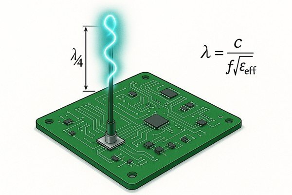
How is PCB antenna length calculated?
Calculating the right antenna length feels like a difficult math problem. If you get it wrong, your device's operating frequency will be off, which kills performance and your link budget. Luckily, it's based on a straightforward physics formula.
Antenna length is calculated based on the signal's wavelength (\(\lambda\)). For a simple monopole antenna, the ideal length is one-quarter of the wavelength (\(\frac{\lambda}{4}\)). The formula is \(\lambda = \frac{c}{f \sqrt{\epsilon_{eff}}}\), where '\(c\)' is the speed of light, '\(f\)' is the frequency, and \(\epsilon_{eff}\) is the effective dielectric constant of the PCB substrate.
The Engineering Details
The calculation for a straight quarter-wave monopole is a great starting point. For 2.45 GHz on FR-4 (\(\epsilon_{eff} \approx 3.2\)), this yields a length of about 17.2 mm. However, most modern devices don't have space for a straight 17 mm trace. This is where more compact designs are used. While the fundamental principle of resonating at a fraction of a wavelength remains, the physical implementation changes. Be cautious when meandering a trace to save space; while it makes the antenna smaller, the sharp bends and close segments create parasitic capacitance, which can significantly reduce radiation efficiency and bandwidth. A slightly larger, straight antenna will almost always outperform a tightly packed, meandering one.
Here is a comparison of common structures:
| Antenna Structure | Key Feature | Pros | Cons |
|---|---|---|---|
| Straight Monopole | Simple \(\frac{\lambda}{4}\) trace | Simple to design, high efficiency, good bandwidth. | Requires the most PCB area. |
| Inverted-F (PIFA) | Folded trace with a shorting pin | Very compact, good performance. | More complex to design and tune. |
| Meandered Trace | A long trace folded into a small area | Extremely small footprint. | Lower efficiency, narrow bandwidth, sensitive to detuning. |
How does PCB material affect PCB antenna performance?
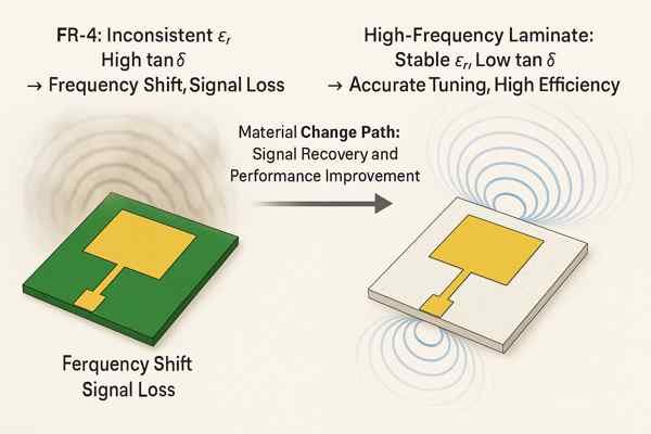
You chose standard FR-4 for your PCB to save costs. But you're finding out that its inconsistent electrical properties at RF frequencies are detuning your antenna and causing unacceptable signal loss.
PCB material directly impacts antenna performance through its dielectric constant (\(\epsilon_{r}\)) and loss tangent (\(\tan\delta\)). An inconsistent \(\epsilon_{r}\) shifts the antenna's resonant frequency, while a high loss tangent absorbs RF energy as heat, reducing the antenna's efficiency and range.
The Engineering Details
Choosing between standard FR-4 and a high-frequency laminate like Rogers is a trade-off between cost, performance, and risk. For a cost-sensitive IoT gadget where "good enough" is the target, FR-4 is often the choice. However, you accept the risk that its \(\epsilon_{r}\) and \(\tan\delta\) vary between batches. This can lead to production units falling out of spec. Another weakness of FR-4 is its higher moisture absorption rate. As it absorbs humidity from the air, its \(\epsilon_{r}\) changes, which can detune the antenna. For a medical device, military hardware, or any high-performance system where reliability is non-negotiable, the extra cost of an RF substrate is easily justified. The stable dielectric properties mean an antenna designed on it will perform predictably from prototype to high-volume production.
Here’s a comparison to put it in perspective:
| Parameter | Standard FR-4 | Rogers RO4350B (RF-Grade) | Impact on Antenna Performance |
|---|---|---|---|
| Dielectric Constant (\(\epsilon_{r}\))3 | \(\approx 4.2 - 4.8\) (variable) | \(3.48 \pm 0.05\) (stable) | A stable \(\epsilon_{r}\) ensures the antenna stays tuned to the correct frequency across all production units. |
| Loss Tangent (\(\tan\delta\))4 | \(\approx 0.02 \text{ @ } 2.4 \text{ GHz}\) | \(\approx 0.0037 \text{ @ } 2.4 \text{ GHz}\) | Lower loss means more power is radiated by the antenna and less is wasted as heat, resulting in higher efficiency. |
| Moisture Absorption | \(\approx 0.15\% - 0.25\%\) | \(\approx 0.06\%\) | Lower absorption leads to more stable performance in varying humidity. |
| Cost | Low ($) | High ($$$) | The choice is a risk management decision balancing unit cost against performance consistency. |
How is PCB antenna performance tested?
Your PCB is back from the fab, and the product is assembled. But how do you know if the antenna actually works well? You can't just ship it and hope for the best; you must test it.
Antenna performance is primarily tested in two ways. First, a Vector Network Analyzer (VNA) measures its return loss (\(S_{11}\)) to verify the 50-\(\Omega\) impedance match. Second, an anechoic chamber is used to measure its radiation pattern, efficiency, and gain.
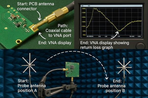
The Engineering Details
Effective testing is a staged process. You can't just test the final assembly and expect to find the root cause of any problems. This methodical approach isolates variables, so if performance drops at a certain stage, you know exactly where the problem lies.
Here is the staged process I use:
| Stage | Objective | Key Metrics & Tools |
|---|---|---|
| 1. Bare PCB | Verify the core antenna design and impedance match. | \(S_{11}\) (Return Loss) using a VNA. Tune the pi-network. |
| 2. With Enclosure | Quantify the detuning effect of the plastic housing. | \(S_{11}\) and Radiation Pattern. Re-tune pi-network if necessary. |
| 3. Full System, Active | Assess real-world performance with digital noise. | \(TRP\) (Total Radiated Power5) & \(TIS\) (Total Isotropic Sensitivity). |
These tests build on each other to provide a complete performance picture. The key test methods are defined below:
| Test Method | What It Measures | Tools Required | Success Criteria (Typical for 2.4 GHz) |
|---|---|---|---|
| Return Loss (\(S_{11}\))6 | Impedance Match Quality | Vector Network Analyzer (VNA) | \(S_{11} < -10 \text{ dB}\) at the operating frequency band. |
| Radiation Pattern & Efficiency7 | Signal directivity, gain, and overall efficiency. | Anechoic Chamber, Turntable | A relatively omnidirectional pattern and efficiency \(> 40\%\). |
| \(TRP\) / \(TIS\) | Active transmit power and receive sensitivity. | Anechoic Chamber, Comms Tester | Meets regulatory and carrier-specific limits (e.g., \(TRP > 20 \text{ dBm}\)). |
What are common PCB antenna layout mistakes?
Your wireless product is failing in the field, and customers are complaining about dropped connections. Simple and avoidable layout mistakes are often the silent killers of RF performance.
The most common mistakes are using an incorrectly sized feedline (not 50 \(\Omega\)), violating the antenna's keep-out zone with ground pours or vias, placing the antenna too close to noisy circuits or metal objects, and using sharp 90-degree bends in RF traces.
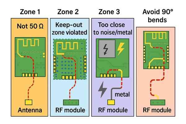
The Engineering Details
I've fixed countless underperforming wireless products, and the issue almost always traces back to a few fundamental layout errors. One of the most valuable yet overlooked features is the pi-network8. Its shunt-series-shunt configuration is incredibly versatile, allowing you to match almost any complex impedance (e.g., \(35+j15 \Omega\)) back to the ideal 50 \(\Omega\). Another subtle but critical mistake is poor ground plane design. The RF return currents from the feedline want to travel directly under the trace. If your ground plane has slots or gaps, these currents have to detour, which creates unwanted inductance and turns your ground plane into an unintentional radiator, causing EMI problems.
Here is a list of errors I frequently find and how to avoid them:
| Mistake | Why It's Bad | How to Fix It |
|---|---|---|
| Incorrect Feedline Width | Causes impedance mismatch and power reflection before the signal even reaches the antenna. | Use an impedance calculator with your PCB manufacturer's stack-up data to get the precise 50 \(\Omega\) trace width. |
| Violating Keep-Out Zone | Placing copper or components near the antenna creates parasitic capacitance that detunes its resonant frequency. | Strictly follow the antenna datasheet's keep-out recommendations on all layers. |
| Poor Ground Stitching | Gaps in the ground plane force RF return currents to take long paths, causing EMI and signal integrity issues. | Use a solid ground plane under RF traces and add plentiful ground stitching vias along the path, especially around bends. |
| No Pi-Network | Lacks the ability to fine-tune the match to compensate for real-world variations. | Always place a 3-component pi-network footprint. You can populate it with 0-ohm resistors initially if the match is close. |
Conclusion
Impedance matching and careful RF layout are not optional details. They are absolutely fundamental to designing a wireless product that works reliably and passes certification, saving you time, money, and frustration.
-
Learn how PIFA antennas balance size and performance, crucial for modern mobile devices. ↩
-
Understanding impedance control is crucial for optimizing RF performance and ensuring compatibility with industry standards. ↩
-
Understanding dielectric constant is crucial for optimizing antenna design and ensuring consistent performance across units. ↩
-
Exploring loss tangent helps in grasping how to enhance antenna efficiency and reduce power loss. ↩
-
Discover the significance of Total Radiated Power in wireless communication systems and improve your design strategies. ↩
-
Understanding Return Loss S11 is crucial for ensuring optimal antenna performance. Explore this link to deepen your knowledge. ↩
-
Learn about the importance of Radiation Pattern and Efficiency in antenna design to enhance your engineering skills. ↩
-
Understanding pi-networks can significantly enhance your RF design skills and help you avoid common pitfalls. ↩


