 Skip to content
Struggling with a design that can't switch fast enough? It’s frustrating when your circuit fails to meet speed requirements, causing delays and forcing redesigns. Let's pinpoint what's holding it back.
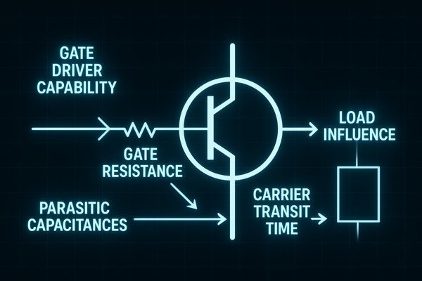
The maximum switching frequency of a transistor is determined by its internal characteristics, such as parasitic capacitances and carrier transit times, along with external circuit factors. These include the gate driver's capability, gate resistance, and the load itself. There isn't a single maximum frequency, but a practical limit defined by these combined factors.
Understanding these limitations is the first step toward designing faster, more efficient circuits. I once worked on a high-frequency power converter for an aerospace application where the prototype failed validation. The MOSFETs were overheating, and we saw significant voltage ringing on the switch node. The root cause wasn't a faulty component, but the interaction between the MOSFET's output capacitance (\(C_{oss}\)) and the parasitic inductance1 of our PCB layout. Fixing it required a deep dive into the very factors we'll discuss here. In this post, I'll share those hard-won lessons to help you navigate these challenges.
What Is the Maximum Switching Frequency for a Transistor?
You see high-frequency numbers on a datasheet but can't achieve them in practice. This gap between theory and reality can lead to unexpected design failures and project delays.
There is no single "maximum switching frequency" for a transistor. Instead, its practical speed is estimated from datasheet parameters like transition frequency (\(f_{T}\)) for BJTs or the switching times (\(t_{r}\), \(t_{f}\)) for MOSFETs. The actual operating frequency is always limited by the application circuit and thermal constraints.
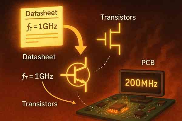
The term "maximum frequency" on a datasheet can be misleading. It usually refers to a specific figure of merit measured under ideal lab conditions. The true limit comes from a combination of the device's physics and your specific circuit implementation.
The True Limiting Factors: Heat and Noise
In the real world, several factors dictate your practical frequency limit long before the silicon gives up. Your final choice will be a compromise based on these competing requirements.
| Limiting Factor | Description | Impact on Maximum Frequency |
|---|---|---|
| Thermal Dissipation | The circuit's ability to remove heat from the transistor's junction (\(T_{J}\)). Switching losses are proportional to frequency. | Major Limiter. Your frequency is capped by the point at which \(T_{J}\) reaches its maximum safe rating. |
| EMI/EMC Compliance | Fast-switching edges create high-frequency noise that can interfere with other electronics and fail regulatory tests. | Often Reduces Frequency. You may need to slow down switching (lower the frequency) to pass EMC certification. |
| Gate Drive Capability2 | The ability of the driver circuit to source/sink enough current to charge/discharge the gate capacitances quickly. | Hard Bottleneck. If the driver can't keep up, the transistor won't switch cleanly, regardless of its own capabilities. |
| PCB Layout Parasitics | Unwanted inductance and capacitance in the PCB traces, especially in the power loop and gate drive loop. | Reduces Usable Frequency. Can cause ringing, overshoot, and instability, forcing you to slow down the design. |
What Is the Unity-Gain Frequency of a Transistor?
The term "unity-gain frequency" or \(f_{T}\) sounds abstract and academic. Ignoring it can lead to poor performance in high-frequency amplifiers or slow switching speeds in power circuits.
The unity-gain frequency, also known as the transition frequency (\(f_{T}\)), is the frequency at which a BJT's common-emitter current gain (\(\beta\) or \(h_{fe}\)) drops to one. It represents the theoretical upper limit of a transistor's useful frequency as an amplifier.
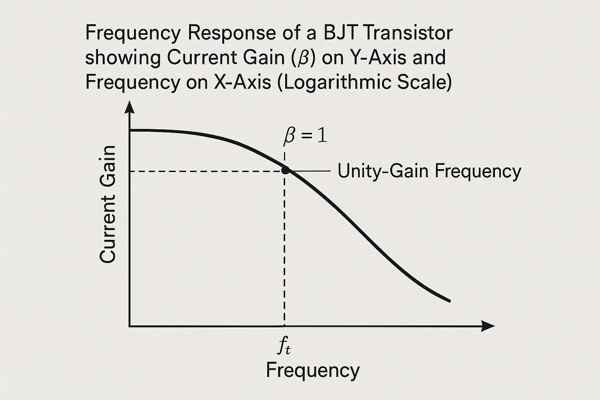
The \(f_{T}\) value is a fundamental figure of merit for a BJT. It gives you a quick way to gauge the intrinsic speed of the device's internal physics. A higher \(f_{T}\) means a faster transistor.
Defining Current Gain (\(\beta\))
First, you have to understand current gain3, or Beta (\(\beta\)). This is the ratio of the output current (Collector Current, \(I_{C}\)) to the input current (Base Current, \(I_{B}\)). A \(\beta\) of 100 means that for every 1 mA of current going into the base, you get 100 mA of current flowing through the collector.
The Impact of Operating Conditions on \(f_{T}\)
A crucial detail many engineers overlook is that \(f_{T}\) is not a static number. It is highly dependent on the transistor's operating point, specifically the collector current (\(I_{C}\)) and collector-emitter voltage (\(V_{CE}\)). Most datasheets for RF transistors include a graph of \(f_{T}\) vs. \(I_{C}\). You will see that \(f_{T}\) peaks at a specific collector current and falls off on either side. For any high-frequency amplifier design, biasing the transistor at this peak \(f_{T}\) point is critical for achieving maximum performance.
How \(f_{T}\) Relates to Switching Speed
While \(f_{T}\) is an amplifier metric, it's a strong indicator of switching performance. A higher \(f_{T}\) implies that the internal capacitances are smaller and the charge carriers move faster across the base region. This allows the transistor to respond more quickly to changes at its input, resulting in faster turn-on and turn-off times. As a reference, this concept is a cornerstone of semiconductor physics taught in texts like "Microelectronic Circuits" by Sedra and Smith.
How Do I Calculate the Maximum Switching Frequency from a Transistor's Datasheet?
Datasheets don't give a single "max frequency" number for switching applications. This leaves you guessing how fast your circuit can actually run, which is a risky way to design.
You can't calculate one absolute maximum frequency. Instead, you estimate the practical switching speed using the rise time (\(t_{r}\)), fall time (\(t_{f}\)), on-delay (\(t_{d(on)}\)), and off-delay (\(t_{d(off)}\)). A simple estimation is \(f_{sw(max)} \approx \frac{1}{t_{r} + t_{f}}\).
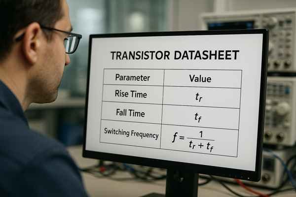
The most reliable method for estimating a MOSFET's speed is to use the switching time values found in its datasheet. But remember, these are always measured under specific test conditions.
The Importance of Test Conditions
The switching times listed in a datasheet are not universal truths. They are measured with a specific gate drive voltage (\(V_{GS}\)), drain current (\(I_{D}\)), and, most importantly, a specific external gate resistor (\(R_{g}\)). If your design uses a different \(R_{g}\), your switching times will change. As a rough rule of thumb, the switching time is proportional to the total gate resistance. If the datasheet specifies times with a 2.5 \(\Omega\) resistor and you use a 10 \(\Omega\) resistor to slow down switching and manage EMI, you can expect your rise and fall times to be roughly 4x longer.
Step-by-Step Calculation with an Example
Let's use a real power MOSFET, the Infineon BSC093N04LS G, as an example. Its datasheet lists the following typical values (tested with \(R_{g} = 2.5 \Omega\)):
| Parameter | Typical Value |
|---|---|
| \(t_{d(on)}\) | 7 ns |
| \(t_{r}\) | 3 ns |
| \(t_{d(off)}\) | 26 ns |
| \(t_{f}\) | 4 ns |
A more conservative calculation considers the entire period: \(T = t_{d(on)} + t_{r} + t_{d(off)} + t_{f}\).
\(T = 7 + 3 + 26 + 4 = 40 \text{ ns}\).
\(f_{sw(max)} = \frac{1}{T} = \frac{1}{40 \times 10^{-9} \text{ s}} = 25 \text{ MHz}\).
Why this Calculation is Only an Estimate
This 25 MHz figure is a theoretical ceiling. In a real power application, running at this frequency would generate catastrophic switching losses. Your actual frequency will be much lower and determined by your thermal design, gate driver capability, and EMI requirements. This calculation provides a starting point for analysis, not a final design value.
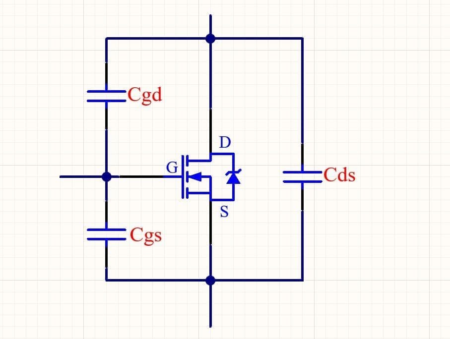
What Are Parasitic Capacitances in a Transistor?
Transistors are not perfect, ideal switches. Unseen internal capacitances can slow down your design, creating bottlenecks and performance issues that are hard to debug after the fact.
Parasitic capacitances are unintentional capacitances that exist between the terminals of a transistor due to its physical semiconductor structure. For a MOSFET, these are the Gate-Source (\(C_{gs}\)), Gate-Drain (\(C_{gd}\)), and Drain-Source (\(C_{ds}\)) capacitances.
You cannot remove these capacitances; they are an inherent part of the device. The goal is to understand them so you can manage their effects.
Breaking Down the Key Capacitances
Datasheets group the physical capacitances into three measurable parameters:
| Datasheet Parameter | Formula | What It Represents |
|---|---|---|
| \(C_{iss}\) (Input) | \(C_{gs} + C_{gd}\) | The capacitance the gate driver "sees." It must be charged to turn the MOSFET on. |
| \(C_{oss}\) (Output) | \(C_{ds} + C_{gd}\) | Affects the drain voltage slew rate and contributes to switching energy loss. |
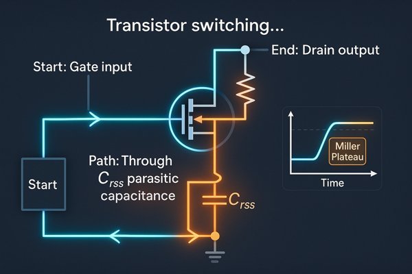
| \(C_{rss}\) (Reverse) | \(C_{gd}\) | The most critical parasitic for switching speed. Also known as the Miller capacitance4. |
The Impact of Non-Linearity (\(C_{oss}\) and \(E_{oss}\))
The voltage dependency of these capacitances has profound effects. The output capacitance, \(C_{oss}\), is particularly non-linear. In hard-switched converters, the energy stored in this capacitance, \(E_{oss} = \int_{0}^{V_{DS}} C_{oss}(V)VdV\), is dissipated as heat every single turn-on cycle. This loss, \(P_{oss} = E_{oss} \times f_{sw}\), becomes a major contributor to total power loss at high voltages and high frequencies. Many modern MOSFET datasheets list the \(E_{oss}\) value at a specific voltage, giving you a much more accurate way to calculate this loss than the simple \(\frac{1}{2}CV^2\) approximation.
How Do Parasitic Capacitances Affect a Transistor's Switching Speed?
Your circuit isn't switching nearly as fast as your calculations predicted. You've checked the logic and component values, but the bottleneck remains. It's almost certainly those parasitic capacitances at work.
Parasitic capacitances must be charged and discharged to switch a transistor on and off. The time required for this process, governed by the available drive current, directly limits the switching speed. The Miller capacitance (\(C_{rss}\)) is especially harmful as it creates a voltage plateau during switching.
The core issue is that you can't change the voltage across a capacitor instantaneously. It takes time and current.
The Effect of Each Parasitic on Performance
Each capacitance plays a different role in degrading switching performance.
| Parasitic Capacitance | Primary Effect | Consequence for Switching Performance |
|---|---|---|
| \(C_{iss}\) (Input) | Must be charged/discharged by the driver. | Determines the total gate charge (\(Q_{g}\)) needed. Larger \(C_{iss}\) requires higher drive current for the same speed. |
| \(C_{rss}\) (Reverse/Miller) | Creates the Miller Plateau. | The main bottleneck for voltage transition speed. Lengthens rise and fall times significantly. |
| \(C_{oss}\) (Output) | Interacts with circuit inductance. Stores energy. | Can cause voltage overshoot and ringing. Stored energy (\(E_{oss}\)) is lost as heat, reducing efficiency. |
Designing the Gate Drive Loop: It's Not Just Capacitance
Beyond capacitance, the parasitic inductance of your gate drive loop is a critical, often-ignored factor. This is the inductance of the physical PCB trace path from the driver output, through the gate resistor, to the MOSFET gate, and back through the source connection to the driver's ground. A high loop inductance will limit the current slew rate (\(di/dt\)) into the gate, effectively choking your driver and slowing down switching, no matter how powerful it is. This is why layout matters: keep your gate driver IC as close as physically possible to the MOSFET, using short, wide traces to minimize this inductance.
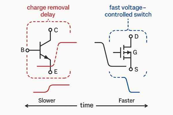
What Is the Difference in Switching Speed Between a BJT and a MOSFET?
Choosing between a BJT and a MOSFET for a high-speed design can be tricky. Making the wrong choice can compromise your circuit's performance, efficiency, and even its physical size.
In general, MOSFETs switch much faster than BJTs of a similar power rating. MOSFETs are voltage-controlled and limited by charging capacitances, while BJTs are current-controlled and limited by the time it takes to remove stored charge from the base region after turn-off.
Their different operating principles are the key to their speed differences.
The Hybrid Solution: IGBTs
What if you need the high voltage/current handling of a BJT but the easier drive of a MOSFET? That's where the Insulated Gate Bipolar Transistor (IGBT)5 comes in. It's a hybrid device that combines a MOSFET input stage with a BJT output stage. This makes IGBTs ideal for high-power applications like motor drives, welding, and solar inverters where raw speed is less critical than power handling.
Head-to-Head Comparison
| Feature | MOSFET | BJT | IGBT |
|---|---|---|---|
| Control Type | Voltage | Current | Voltage |
| Primary Speed Limiter | Gate Capacitance | Charge Storage | Tail Current |
| On-State Loss | Resistive (\(R_{DS(on)}\)) | Low saturation voltage (\(V_{CE(sat)}\)) | Low saturation voltage (\(V_{CE(sat)}\)) |
| Typical Frequency | Very High (MHz+) | Low-Medium (kHz) | Medium (\(<100 \text{ kHz}\)) |
| Application Niche | High-freq SMPS, DC-DC | Low-cost, low-freq switching | High-power, medium-freq drives |
How Does a Gate Driver Circuit Affect the Switching Speed of a MOSFET?
You selected a top-of-the-line, fast-switching MOSFET, but your circuit is still sluggish. The design isn't meeting its speed or efficiency targets, and you're not sure why. The problem is likely your gate driver.
A gate driver is a power amplifier for the MOSFET gate. It provides the high peak currents needed to rapidly charge and discharge the gate capacitances. The driver's current sourcing/sinking capability and low output impedance directly determine the switching time and speed.
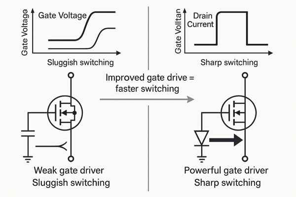
The gate of a MOSFET is essentially a capacitor. Driving it requires significant current for short bursts, something a standard microcontroller pin cannot do.
Impact of Gate Drive Parameters on Performance
| Parameter | What it Does | Impact of a "Better" Value (e.g., Higher Current) |
|---|---|---|
| Peak Source/Sink Current | The maximum current the driver can provide to the gate. | Faster Switching. Directly reduces the time to charge/discharge the gate. |
| Output Impedance (\(R_{out}\)) | The internal resistance of the driver's output stage. | Faster Switching. A lower \(R_{out}\) allows more current to flow and reduces voltage drop. |
| Propagation Delay | The internal delay from the driver's input to its output. | More Precise Timing. A lower delay is critical for high-frequency and multi-phase systems. |
| External Gate Resistor (\(R_{g}\)) | A user-added resistor to control switching speed. | Trade-off. A smaller \(R_{g}\) speeds up switching but increases EMI and ringing. A larger \(R_{g}\) does the opposite. |
Pro-Tip: Asymmetric Gate Drive
For advanced control, you can use asymmetric gate drive. This involves using different resistance values for turn-on and turn-off.
- Fast Turn-On: Use a small gate resistor to quickly charge the gate and minimize turn-on losses.
- Slower Turn-Off: Use a larger gate resistor for turn-off. This slows the \(dV/dt\) rate, which can significantly reduce voltage overshoot and ringing caused by parasitic inductance in the power loop.
This is easily implemented by placing a diode in parallel with the turn-on resistor. Current flows through the small resistor during turn-on, but is forced through a second, larger resistor during turn-off when the diode is reverse-biased.
What Is the Trade-off Between Switching Speed and Power Dissipation in a Transistor?
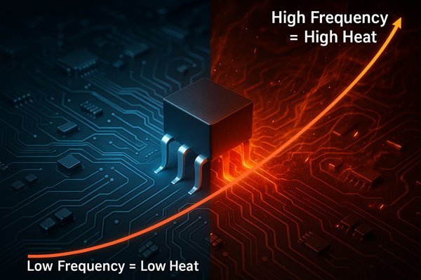
You want to design the fastest switching circuit possible to shrink the size of your components. But as you push the frequency higher, your transistor starts to overheat and threatens to fail.
The fundamental trade-off is that higher switching frequencies lead to proportionally higher switching losses. These losses occur during the rise and fall times when the transistor acts like a resistor, simultaneously conducting current and supporting voltage, which generates significant heat.
This creates a critical design trade-off that every power electronics engineer faces.
The Designer's Dilemma: A Balancing Act
| Aspect | Higher Switching Frequency | Lower Switching Frequency |
|---|---|---|
| Passive Components | Pro: Smaller, cheaper inductors and capacitors. | Con: Larger, more expensive passive components. |
| Power Density | Pro: More power in a smaller physical volume. | Con: Lower power density. |
| Efficiency | Con: Higher switching losses (\(P_{sw}\)) reduce efficiency. | Pro: Lower switching losses improve efficiency. |
| Thermal Management | Con: More heat generated, requires a more robust cooling solution. | Pro: Less heat generated, simpler cooling. |
| EMI/Ringing | Con: Sharper edges create more high-frequency noise and voltage overshoot. | Pro: Softer switching produces less EMI and ringing. |
| Transient Response | Pro: Faster control loop response to load changes. | Con: Slower control loop response. |
Breaking the Trade-off with Soft Switching
Is it possible to have both high frequency and high efficiency? Yes, with advanced circuit topologies. Techniques like Zero-Voltage Switching (ZVS)6 and Zero-Current Switching (ZCS)7 are designed to break this trade-off. They use resonant LC tanks to shape the voltage and current waveforms so that the transistor switches when either the voltage across it or the current through it is zero. This nearly eliminates the switching loss, allowing for a dramatic increase in operating frequency without the thermal penalty. This is the key technology behind many high-density power converters.
How Do I Choose the Right Transistor for a High-Frequency Application?
Faced with thousands of transistor options from dozens of manufacturers, how do you pick the right one? Choosing a suboptimal component can doom your design's performance and efficiency from the very start.
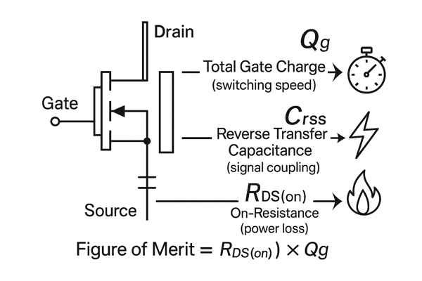
For high-frequency applications, focus on selecting a MOSFET with low total gate charge (\(Q_{g}\)), low reverse transfer capacitance (\(C_{rss}\)), and low on-resistance (\(R_{DS(on)}\)). Using a Figure of Merit (FOM), like \(R_{DS(on)} \times Q_{g}\), helps compare devices directly.
Here is a systematic checklist to narrow down the choices and find the best fit.
Transistor Selection Checklist
| Parameter | What to Look For | Why It's Important |
|---|---|---|
| \(V_{DS(max)}\) | > Max Bus Voltage + 30% safety margin. | Prevents device failure from voltage spikes and transients. |
| \(I_{D(max)}\) | > Max Peak Current in the circuit. | Ensures the transistor can handle the worst-case current load. |
| \(Q_{g}\) (Total Gate Charge) | As low as possible. | Lower \(Q_{g}\) means less work for the gate driver, enabling faster switching and lower drive losses. |
| \(R_{DS(on)}\) | As low as possible for your voltage class. | Lower \(R_{DS(on)}\) directly reduces conduction losses (\(P=I^2R\)). |
| FOM (\(R_{DS(on)} \times Q_{g}\)) | The lowest value available. | A lower FOM indicates a technologically superior device with a better balance of losses. |
| \(C_{rss}\) | As low as possible. | A lower Miller capacitance shortens the Miller plateau, directly increasing switching speed. |
| Package | Leadless (QFN, DFN) or low-inductance packages. | Minimizes parasitic inductance, which is a primary cause of voltage ringing and EMI. |
| \(E_{AS}\) (Avalanche Rating) | A high value for ruggedness. | Indicates the device's ability to survive inductive voltage spikes, improving reliability. |
Conclusion
A transistor's maximum switching frequency is not one number but a dynamic limit. It's set by a careful balance of the device's internal physics and the design of the external circuit.
-
Learn about parasitic inductance and its implications in PCB design to improve your circuit efficiency and reliability. ↩
-
Gate drive capability is essential for efficient switching in transistors. Discover more about its significance in this informative link. ↩
-
Understanding current gain is essential for optimizing transistor performance in circuits. Explore this link for a deeper insight. ↩
-
Learning about Miller capacitance can enhance your understanding of switching speed and efficiency in MOSFETs. ↩
-
Explore the benefits of IGBTs in high-power applications, including their efficiency and versatility in various industries. ↩
-
Explore this link to understand how ZVS can enhance efficiency in power converters, reducing losses and improving performance. ↩
-
Learn about ZCS and its advantages in minimizing switching losses, crucial for efficient power management. ↩


