 Skip to content
Struggling with your high-speed design? The wrong PCB material can introduce signal loss and impedance mismatches, causing your project to fail validation and delaying your schedule.
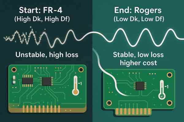
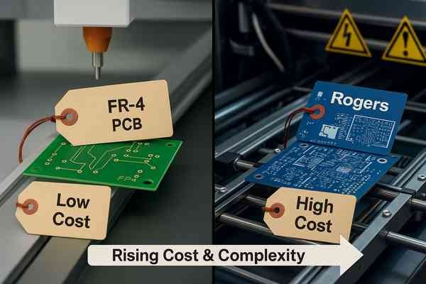
The primary differences are dielectric constant (\(D_{k}\)), dissipation factor (\(D_{f}\)), thermal stability, and cost. Standard FR-4 is inexpensive but has high, unstable electrical loss above \(1 \text{ GHz}\). High-frequency laminates like Rogers materials offer low, stable loss but at a significantly higher price point.
Choosing the right PCB substrate is one of the most fundamental decisions in hardware design. It's the foundation upon which your entire circuit is built. While FR-4 is the default for a huge range of applications, the moment you step into the world of high-speed digital or RF design, the game changes completely. This decision isn't just a line item on a BOM; it's an engineering commitment that impacts performance, reliability, and manufacturability. Let's walk through the structured decision-making process for selecting the right material for your project.
What are the criteria for selecting a PCB dielectric material?
Picking a dielectric can feel overwhelming with so many options. A poor choice can easily compromise your circuit's performance, blow your budget, and set you back weeks.
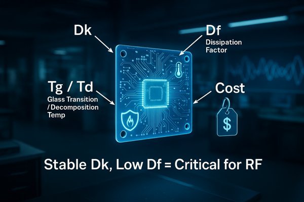
Key selection criteria are dielectric constant (\(D_{k}\)), dissipation factor (\(D_{f}\)), operating frequency, thermal properties like Glass Transition Temperature (\(T_{g}\)) and decomposition temperature (\(T_{d}\)), and overall cost. For high-speed or RF designs, a stable \(D_{k}\) and low \(D_{f}\) are absolutely critical.
When I start a new design, I evaluate materials by comparing their core properties side-by-side. A table is the best way to see the trade-offs clearly. Here is a typical comparison I would make:
| Property | Standard FR-4 (IPC-4101/21) | High-Performance FR-4 (IPC-4101/126)1 | High-Frequency (Rogers RO4350B) |
|---|---|---|---|
| Glass Transition Temp (\(T_{g}\)) | \(\approx 140^\circ\text{C}\) | \(\approx 180^\circ\text{C}\) | \(>280^\circ\text{C}\) (No Tg) |
| Decomposition Temp (\(T_{d}\)) | \(\approx 300^\circ\text{C}\) | \(\approx 345^\circ\text{C}\) | \(\approx 390^\circ\text{C}\) |
| Z-axis CTE (below \(T_{g}\)) | \(\approx 60 \text{ ppm}/^\circ\text{C}\) | \(\approx 50 \text{ ppm}/^\circ\text{C}\) | \(\approx 30 \text{ ppm}/^\circ\text{C}\) |
| Dielectric Constant (\(D_{k}\))2 | 4.5 (at 1 MHz) | 3.8 (at 2 GHz) | 3.48 (at 10 GHz) |
| Dissipation Factor (\(D_{f}\)) | 0.020 (at 1 MHz) | 0.010 (at 2 GHz) | 0.0037 (at 10 GHz) |
This table immediately highlights the advantages of moving to a higher-grade material. The improved thermal stability (higher \(T_{g}\) and \(T_{d}\), lower CTE) of high-performance FR-4 makes it suitable for lead-free assembly and improves via reliability. For RF work, however, the superior and more stable electrical properties (\(D_{k}\) and \(D_{f}\)) of a material like Rogers are non-negotiable. Notice how the test frequencies for \(D_{k}\) and \(D_{f}\) differ; this is because manufacturers characterize materials for their intended application range.
What are the detailed steps of selecting a right PCB dielectric material?
Knowing the criteria is one thing, but applying them can be confusing. This can lead to over-specifying and wasting money or under-specifying and causing design failure.
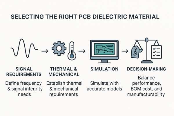
First, define frequency and signal integrity needs. Next, establish thermal and mechanical requirements. Then, simulate using accurate models. Finally, balance performance against BOM cost and manufacturability by comparing qualified materials and consulting your fabrication partner for their input.
Over my career, I've developed a systematic process to avoid guesswork. Following these steps ensures all key factors are considered, leading to a choice that is both technically sound and commercially viable.
Step 1: Define Electrical Performance Requirements.
This is always the starting point. You must clearly define the electrical budget for your critical signals.
- Maximum Frequency: What is the highest frequency component of your signals? This immediately puts you into a material category.
- Impedance Control3: What is your target impedance (e.g., \(50 \Omega\) single-ended) and what tolerance is required (\(\pm 10\%\) or tighter)?
- Loss Budget: What is the maximum acceptable insertion loss (\(IL\))? An RF design might have a budget of \(<3 \text{ dB}\).
Step 2: Determine Thermal and Mechanical Constraints.
Next, consider the physical world the PCB will live in.
- Manufacturing Process: Will the board undergo lead-free reflow? If so, a material with a \(T_{g} > 170^\circ\text{C}\) and \(T_{d} > 340^\circ\text{C}\) is essential.
- Operating Environment: What is the product's operational temperature range? For automotive or aerospace applications (IPC Class 3), a low Z-axis CTE is critical for via reliability.
Step 3: Simulate with Accurate Material Models.
Before shortlisting, verify your choice with simulation. Obtain accurate material data (wideband \(D_{k}/D_{f}\) values or S-parameter models) from the material vendor. Use a field solver or tool like Ansys HFSS or Keysight ADS to model your critical channels. This step validates that your chosen material will meet your loss budget and impedance targets before you even talk to a fab house.
Step 4: Create a Shortlist and Evaluate Total Cost.
With a validated choice, create a shortlist of 2-3 candidate materials. Engage your PCB fabricator to get quotes. Remember to evaluate the total cost, which includes raw materials and any special processing fees.
Step 5: Consult with Your Fabrication Partner.
This is a critical final check. I never finalize a material without talking to my fab house. They provide invaluable feedback on manufacturability, suggest stock alternatives, and can confirm their ability to process your specific stackup.
FR-4 vs. Rogers material: When should each type be used?
Are you debating between standard FR-4 and an expensive Rogers material? Choosing wrong means either over-engineering and wasting money or under-engineering and failing validation tests.
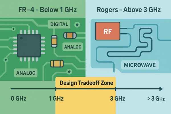
Use FR-4 for frequencies below \(1 \text{ GHz}\) and for most digital or low-frequency analog circuits. Switch to Rogers or similar high-frequency materials for applications above \(3 \text{ GHz}\), especially for RF, microwave, and critical high-speed digital designs where low signal loss is mandatory.
To make the decision even clearer, I've expanded the comparison table to include high-performance FR-4, which often represents the best compromise between cost and performance.
| Parameter | Standard FR-4 | High-Performance FR-4 | Rogers (RO4350B) |
|---|---|---|---|
| Typical Max Frequency | \(<1 \text{ GHz}\) | \(1 - 5 \text{ GHz}\) | \(>20 \text{ GHz}\) |
| Signal Loss | High | Medium | Very Low |
| Impedance Stability | Fair | Good | Excellent |
| Relative Cost | \(1\text{x}\) | \(1.5\text{x} - 3\text{x}\) | \(5\text{x} - 20\text{x}\) |
| Best For | General purpose, low-cost electronics, power supplies. | High-layer count boards, servers, DDR memory, cost-sensitive \(>1\text{GHz}\) designs. | RF/Microwave, antennas, high-speed backplanes, test equipment. |
The "gray area" is where high-performance FR-4 shines. For many projects, this material class provides the necessary signal integrity without the extreme cost of RF laminates. I often use hybrid stackups to optimize this trade-off. Here is an example of a 6-layer stackup for a device with a Wi-Fi module:
| Layer | Function | Material | Approx. Thickness |
|---|---|---|---|
| L1 | RF Traces / Antenna | Rogers RO4350B | 0.254 mm |
| L2 | Ground Plane | Prepreg | 0.150 mm |
| L3 | High-Speed Digital | Isola 370HR | 0.200 mm |
| L4 | Power Plane | Isola 370HR | 0.200 mm |
| L5 | Ground Plane | Prepreg | 0.150 mm |
| L6 | Low-Speed Digital | Isola 370HR | 0.500 mm |
This design strategically places the expensive RF material only where needed, on the outer layer, while using cost-effective high-performance FR-4 for the digital core.
How does the choice of dielectric material affect signal integrity?
Chasing down signal integrity issues is a hardware engineer's nightmare. You spend days in the lab trying to fix reflections or losses, only to find the problem is baked into the PCB itself.
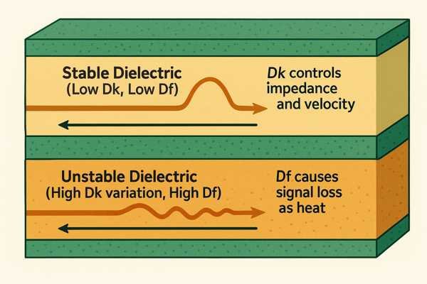
The dielectric material is fundamental to signal integrity. Its dielectric constant (\(D_{k}\)) determines trace impedance and signal velocity, while its dissipation factor (\(D_{f}\)) dictates how much signal energy is lost as heat. Unstable materials cause reflections, timing skew, and attenuation.
Total signal loss is a sum of dielectric loss and conductor loss. While we've focused on the dielectric, the conductor becomes equally important at very high frequencies.
Dielectric Loss and Fiber Weave
As discussed, dielectric loss4 is governed by \(D_{f}\), and the fiber weave effect can introduce skew. Using tighter weaves like 1080 or 106 is a key mitigation strategy for multi-gigabit differential pairs.
Conductor Loss: Skin Effect and Surface Roughness
At high frequencies, current no longer flows through the entire conductor. Due to the skin effect5, it concentrates in a thin layer near the surface. The skin depth (\(\delta\)) decreases with frequency, making the effective cross-sectional area smaller and increasing resistance. Furthermore, the current path follows the rough profile of the copper foil's surface. A rougher surface increases the path length, further increasing loss. This is why specifying low-profile (LP) or very-low-profile (VLP) copper is critical for designs above 10 GHz.
| Copper Foil Type | Typical Roughness (\(R_{z}\)) | Impact on Loss @ 28 GHz |
|---|---|---|
| Standard (STD) | \(5-10 \text{ } \mu\text{m}\) | High |
| Low Profile (LP) | \(\approx 3 \text{ } \mu\text{m}\) | Medium |
| Very Low Profile (VLP) | \(\approx 1.5 \text{ } \mu\text{m}\) | Low |
| Reverse Treated Foil (RTF) | \(3-5 \text{ } \mu\text{m}\) | Medium (Good compromise) |
For my most critical designs, specifying a VLP copper on a low-loss laminate is a standard requirement to meet the loss budget.
How does the choice of dielectric material impact overall PCB cost and manufacturing?
Your design works perfectly in simulation. But then the manufacturing quote for your high-frequency material comes back and completely shatters your project's budget.
High-frequency laminates like Rogers can cost 5 to 20 times more than standard FR-4 per unit area. They also require specialized manufacturing processes and tooling, increasing fabrication complexity, lead time, and cost.
Balancing performance with cost is a core responsibility. The cost impact is felt in the raw material price and in the additional manufacturing steps required.
- Raw Material Cost: This is the most obvious difference. A panel of Rogers material can cost over ten times more than an equivalent panel of FR-4.
- Manufacturing Complexity and Yield: The costs don't stop at raw material.
- Tooling and Drilling: Abrasive ceramic-filled RF materials wear out drill bits much faster than FR-4, requiring more frequent tool changes and increasing cost.
- Lamination: Lamination cycles for dissimilar materials in a hybrid stackup are complex and require tight process control to prevent delamination or warping, which can impact yield.
- Via Formation: For extremely high-speed designs, techniques like back-drilling are used to remove unused via stubs that cause reflections. This is an extra process step that adds significant cost but is often necessary for 25+ Gbps channels.
What are the relevant IPC standards for PCB base materials?
You specified a "high-performance" material on your fab drawing. But what does that really mean? Without a standard, you're likely to get inconsistent quality and unpredictable results.
The most important standard is IPC-4101, Specification for Base Materials for Rigid and Multilayer Printed Boards. It classifies laminates using "slash sheets" (e.g., /21, /126) that define electrical, thermal, and mechanical properties, ensuring consistency between suppliers.
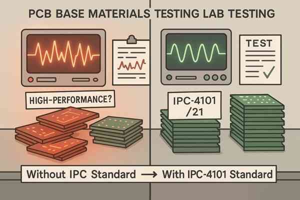
Relying on standards replaces ambiguity with precise, verifiable requirements. I always call out the specific IPC-4101 slash sheet on my fabrication notes.
| Slash Sheet | Material Description | Key Parameters | Typical Application |
|---|---|---|---|
| IPC-4101/21 | Standard FR-4, Epoxy | \(T_{g} \text{ } 110-150^\circ\text{C}\) | Low-cost consumer electronics, general use. |
| IPC-4101/26 | Halogen-Free FR-4 | \(T_{g} >150^\circ\text{C}\), Halogen-Free | Environmentally compliant products (RoHS). |
| IPC-4101/126 | High-Performance FR-4 | \(T_{g} >170^\circ\text{C}\), \(T_{d} >340^\circ\text{C}\) | Lead-free assembly, servers, high-speed digital. |
| IPC-4101/129 | High-Performance FR-4 | \(T_{g} >170^\circ\text{C}\), Enhanced Stability | Similar to /126 but with enhanced thermal stability. |
By specifying /126, you guarantee a material that can withstand lead-free reflow and provides more consistent electrical performance. The IPC-TM-650 Test Methods Manual6 defines the procedures for measuring properties for all material types. The board's overall reliability class is defined in IPC-22217.
What are the future trends in PCB dielectric materials?
Thinking your material choice is safe? The demands of next-generation electronics, from 6G to AI accelerators, are pushing traditional materials to their absolute limits.
Future trends are focused on ultra-low loss materials for data rates over 112 Gbps, improved thermal management for high-power components, and new composites that offer better performance and manufacturability for applications like automotive radar and satellite communications.

As an engineer, it's crucial to keep an eye on what's next. The material I select today might not be sufficient for a project two years from now. I am closely watching developments in several key areas:
| Material Trend | Key Properties | Target Application |
|---|---|---|
| Ultra-Low Loss (ULL) | \(D_{f} < 0.002\) | 112/224 Gbps PAM4 signaling, high-speed backplanes. |
| High Thermal Conductivity | \(TC > 1.0 \text{ W/mK}\) | High-power RF amplifiers, LED lighting, power modules. |
| Glass-Free Laminates | Extremely uniform \(D_{k}\) | Millimeter-wave (mmWave) applications, 6G, advanced radar. |
| Low-CTE Composites | CTE matched to silicon | Chip-on-board (CoB), advanced packaging, space applications. |
These advancements are critical. For instance, as data rates double, the acceptable signal loss budget is halved, making materials with a \(D_{f}\) below 0.002 a necessity, not a luxury. Similarly, as GaN and SiC power devices become more common, materials with high thermal conductivity (\(TC\)) will be essential for pulling heat away from these components. Staying informed on these trends is key to designing competitive products.
Conclusion
The choice between FR-4 and high-frequency laminates is a trade-off. Use FR-4 for cost-driven designs under \(1 \text{ GHz}\). For high-performance applications, invest in advanced laminates to guarantee signal integrity.
-
Explore the advantages of High-Performance FR-4 for improved thermal stability and reliability in PCB applications. ↩
-
Learn how the Dielectric Constant impacts signal integrity and performance in PCB designs. ↩
-
Impedance control is vital for signal integrity in PCBs; learning more can improve your design outcomes significantly. ↩
-
Dielectric loss is a key factor in signal integrity. Learn more about its implications for high-frequency designs by exploring this resource. ↩
-
Understanding the skin effect is crucial for optimizing conductor designs, especially at high frequencies. Explore this link for in-depth insights. ↩
-
Learn about the IPC-TM-650 test methods to see how they validate material properties and ensure compliance with industry standards. ↩
-
Discover the IPC-2221 standard to understand how it impacts the design and reliability of electronic circuit boards. ↩


