
Struggling with timing errors in your digital design? Your clock signal might be too weak to drive all the components, causing system instability and weird crashes.
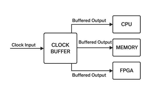
A clock buffer is a specialized integrated circuit (IC) that takes a single clock signal as input and produces multiple copies. These copies have the same frequency and phase but with restored signal quality and increased drive strength for circuits with many components.
Driving a clean, synchronized clock signal to every part of your circuit is one of the most fundamental challenges in hardware engineering. I’ve learned this lesson on countless projects, from industrial controllers to complex SoCs. When you have many devices that all need the same clock, you can’t just split the signal trace on your PCB and hope for the best. The signal will degrade quickly. This is where a clock buffer becomes an essential tool in your design toolkit. Let’s break down exactly why these components are so critical.
Why Are Clock Buffers Necessary?
Does your system crash unpredictably? A weak clock signal failing to reach all ICs at the same time could be the culprit, leading to intermittent failures.
Clock buffers are necessary to provide the required drive current (fan-out) for a clock signal that’s distributed to many different loads. They regenerate the signal, ensuring it has sharp edges and correct voltage levels, which prevents timing violations and ensures reliable system operation.
The Problem of Signal Degradation
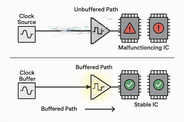
In any digital system, the clock signal is the heartbeat. It tells every component when to act. The source of this clock, like a crystal oscillator or a processor pin, has a limited ability to drive a signal. At high frequencies, the PCB trace itself starts acting like a transmission line. Splitting this trace creates impedance mismatches, which cause signal reflections1 that further distort the clock waveform.
Restoring Signal Integrity
A clock buffer acts as a regenerating hub. It properly terminates the incoming clock and uses its powerful drivers to create multiple new, pristine copies. The difference between an ideal clock and one degraded by high fan-out is stark.
| Characteristic | Ideal Clock Signal | Degraded Signal (from Overload) |
|---|---|---|
| Waveform Shape | Perfect square wave | Rounded, distorted shape |
| Rise/Fall Time | Very fast (e.g., \(< 500 \text{ ps}\)) | Slow (e.g., \(> 2 \text{ ns}\)) |
| Voltage Levels | Reaches full VCC and GND | Fails to reach valid \(V_{OH}\)/\(V_{OL}\) |
| Noise Margin | High | Low, susceptible to noise |
This table shows exactly what a clock buffer fixes: it takes a degraded signal and restores its characteristics back to the ideal state, ensuring reliable operation.
What Is Clock Fan-Out in a Digital Circuit?
Have you ever wondered why simply splitting a clock trace causes so many problems? You are most likely exceeding the clock source’s fan-out limit, which leads to a degraded and unreliable signal.
Clock fan-out is the maximum number of digital inputs that the output of a single clock source can reliably drive. Exceeding this limit causes serious signal integrity issues like slow rise times and reduced voltage levels, because the source simply cannot provide enough current for all the loads.

Fan-Out in CMOS Logic
In modern CMOS technology, fan-out is all about capacitive loading. Every IC input pin has a small input capacitance, typically 2 \(\text{pF}\) to 7 \(\text{pF}\). This adds up quickly when you connect multiple devices.
Calculating Load
The ability of a driver to charge this total capacitance determines the signal’s rise and fall time. The relationship is described by the formula \(I = C \frac{dV}{dt}\). Here, \(I\) is the drive current from the source, \(C\) is the total capacitance of all the loads, and \(\frac{dV}{dt}\) is the rate of voltage change. For a fixed drive current \(I\), a larger total capacitance \(C\) means that \(dt\) (the rise time) must increase. This progression is predictable and shows why fan-out is a critical design constraint.
| Number of Loads | Input Capacitance per Load | Trace Capacitance (Est.) | Total Load Capacitance | Impact on Signal |
|---|---|---|---|---|
| 1 | 5 \(\text{pF}\) | 2 \(\text{pF}\) | 7 \(\text{pF}\) | Sharp edges, good integrity |
| 5 | 5 \(\text{pF}\) | 10 \(\text{pF}\) | 35 \(\text{pF}\) | Slower edges, reduced margin |
| 10 | 5 \(\text{pF}\) | 20 \(\text{pF}\) | 70 \(\text{pF}\) | Very slow edges, timing failures |
What Are the Consequences of Not Using a Clock Buffer in a High-Fan-Out Design?
Are you chasing phantom bugs in your system? Ignoring high fan-out can lead to erratic behavior that is almost impossible to trace back to its root cause: a failing clock signal.
Not using a clock buffer in a high-fan-out design leads to severe signal degradation. This results in slow signal edges, a reduced noise margin, increased clock skew, and ultimately, setup and hold time violations. Your system will become unreliable, with data corruption and unpredictable crashes.

Timing Violations
I once spent a week debugging a prototype where a junior engineer had split a clock signal with a T-junction. The resulting signal degradation and skew were just enough to cause intermittent setup time violations. A single clock buffer IC fixed the problem completely. If a chip requires a data signal to be stable for 200 picoseconds (setup time) before the clock edge, but your clock skew is 150 \(\text{ps}\), you now only have a 50 \(\text{ps}\) window for everything else.
System-Level Instability
These low-level issues cascade into system-wide failures. The root causes are simple physics, but the impact is catastrophic for the product’s reliability.
| Root Cause | Direct Signal Consequence | System-Level Impact |
|---|---|---|
| Excessive Capacitive Load | Slow Rise/Fall Times | Setup/Hold Violations, Metastability |
| Unmatched Trace Impedances | Signal Reflections, Ringing | False Clock Edges, Data Corruption |
| Unequal Path Lengths | High Clock Skew | Reduced Timing Margins, Race Conditions |
This chain of events shows how a single layout mistake—overloading a clock output—can lead to complete system failure.
What Are Clock Skew and Clock Jitter?
Are the timing margins in your high-speed design razor-thin? Misunderstanding the difference between skew and jitter can lead to designs that fail in mass production, even if the prototype worked on your bench.
Clock skew is the time difference when the same clock edge arrives at different components. Clock jitter is the variation in a clock signal’s timing from its ideal position over time. Skew is a spatial problem (different places), while jitter is a temporal problem (different times).

Skew: The Spatial Problem
If the trace to IC A is 5 \(\text{cm}\) long and the trace to IC B is 7 \(\text{cm}\) long, there will be a predictable skew between them. A good design rule is to keep skew between critical components below 50-100 \(\text{ps}\). This is why PCB layout tools have features to add serpentine bends to shorter traces to match the length of the longest one.
Jitter: The Temporal Problem
Jitter is a dynamic problem caused by noise. If you look at a clock on an oscilloscope, the edges seem to "wobble" back and forth slightly. For high-speed serial links like PCIe Gen 4, the reference clock jitter must be \(< 0.5 \text{ ps RMS}\), according to the PCIe Base Specification.
| Characteristic | Clock Skew | Clock Jitter |
|---|---|---|
| Domain | Spatial (between different points) | Temporal (at one point over time) |
| Nature | Deterministic (caused by layout) | Random (caused by noise) |
| Analogy | Two runners arriving at different times | A single runner with an unsteady pace |
| Mitigation | Matched-length routing, clock buffers | Low-noise power supplies, good shielding |
How Does a Clock Buffer Minimize Skew and Improve Signal Integrity?
Struggling to synchronize dozens of ICs across a large PCB? A well-placed clock buffer is the key to solving your timing headaches, ensuring every component gets a clean clock right on time.
A clock buffer minimizes skew by providing multiple outputs with precisely matched propagation delays from a central point. It improves signal integrity by regenerating the clock, producing sharp, fast edges and a full voltage swing, which effectively restores the signal’s quality for all loads.
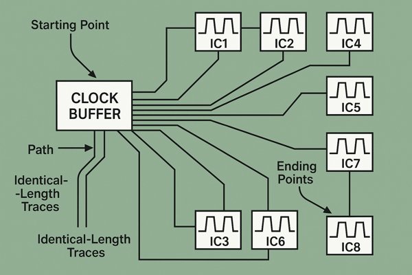
Advanced Clock Distribution Topologies
A clock buffer enables disciplined layout strategies. The most common is the star topology2. For more demanding applications, like on a large FPGA or an ASIC, an H-tree3 distribution network is used to ensure the path length from the central buffer to any endpoint is identical, virtually eliminating layout-induced skew.
Zero-Delay Buffers and Matched Outputs
High-performance clock buffers like the Texas Instruments LMK00334 specify a part-to-part output skew of just 35 \(\text{ps}\). This precision allows you to confidently distribute a clock, knowing the timing relationship between all components is tightly controlled. They are purpose-built to solve common timing problems.
| Problem | Clock Buffer Solution | Resulting Benefit |
|---|---|---|
| High Fan-Out / Capacitive Load | High-Drive Output Stages | Sharp, fast signal edges; full voltage swing |
| Clock Skew | Matched-Delay Outputs & Zero-Delay PLL | Synchronized signal arrival across all ICs |
| Signal Degradation (Noise, etc.) | Internal Signal Regeneration | Restored signal integrity and noise margin |
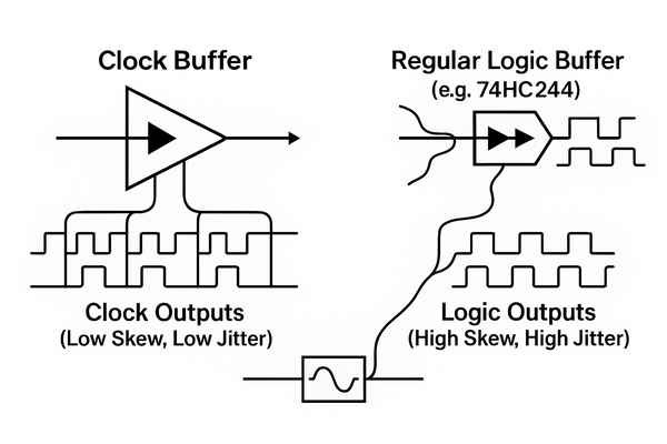
What Is the Difference Between a Clock Buffer and a Regular Logic Buffer?
Thinking of using a standard logic buffer, like a 74HC244, as a clock buffer to save a few cents? This common mistake can introduce massive amounts of jitter and skew, completely wrecking your design’s timing.
A clock buffer is specifically engineered for precision timing, with very low skew between outputs and extremely low additive jitter. A regular logic buffer is a general-purpose part not optimized for these characteristics. Its main job is simple logic level restoration, not high-fidelity clock distribution.
Designed for Timing and Power Integrity
A key difference is the power supply design. High-performance clock buffers often have separate analog power pins (AVDD) for their internal PLLs. These require careful filtering to isolate them from digital noise, which is crucial for minimizing jitter. A logic buffer just has a single VCC pin.
General-Purpose Functionality
A regular logic buffer’s propagation delay4 can vary by several nanoseconds from one channel to another. This is, by definition, skew. The datasheet tells the story.
| Parameter | Dedicated Clock Buffer | Regular Logic Buffer (e.g., 74HC244) |
|---|---|---|
| Primary Goal | Timing precision, low skew/jitter | Logic isolation, current drive |
| Output-to-Output Skew | Very low (e.g., \(< 50 \text{ ps}\)) | High, often not specified |
| Additive Jitter | Very low (e.g., \(< 100 \text{ fs RMS}\)) | High, not specified |
| Power Supply Pins | Often has separate, filtered AVDD | Single VCC, no special filtering |
| Cost | Higher | Lower |
On any serious project, saving 30 cents on a component is pointless if it leads to weeks of debugging.
Conclusion
Using a dedicated clock buffer is not an optional luxury in high-fan-out or high-speed digital designs. It’s a fundamental requirement for ensuring system stability and timing integrity.
-
Exploring signal reflections will help you grasp their impact on signal quality and how to mitigate issues in PCB design. ↩
-
Understanding star topology is crucial for effective clock distribution in digital circuits, enhancing design efficiency. ↩
-
Exploring H-tree distribution networks can provide insights into minimizing skew and optimizing performance in complex designs. ↩
-
Exploring propagation delay helps in grasping its impact on circuit timing and overall functionality, essential for effective design. ↩


