
Struggling with clock signal integrity? Distributing a clean clock to multiple chips can be a nightmare, causing system instability and timing failures.
No, they are essentially the same. A fan-out buffer is a type of clock buffer specifically designed to take one clock input and distribute it to multiple outputs. The terms are often used interchangeably to describe a device that creates multiple, clean copies of a single clock source.
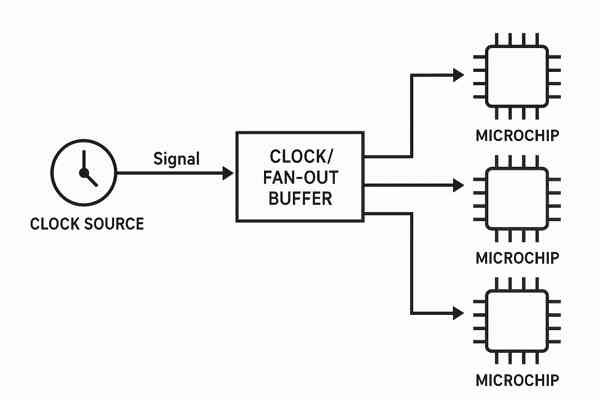
Now that we know they’re basically the same thing, let’s explore when to use different types and what to look for. This might seem simple, but I’ve seen many projects delayed because of poor clock distribution. The wrong choice can lead to intermittent failures that are incredibly difficult to debug. Understanding the details is key to building a robust timing system in any design, and getting it right from the start will save you a lot of headaches later.
When Is a Standard Single-Ended (LVCMOS) Clock Buffer Sufficient?
Your system seems simple, but clock noise is causing random errors? Is an expensive differential buffer always necessary, or will a basic LVCMOS buffer do the job?
A standard single-ended (LVCMOS) clock buffer is sufficient for low-to-moderate frequency applications, typically \(\approx <200 \text{ MHz}\). It works best when clock paths are short, noise is low, and you’re driving other LVCMOS inputs on the same PCB without crossing connectors.
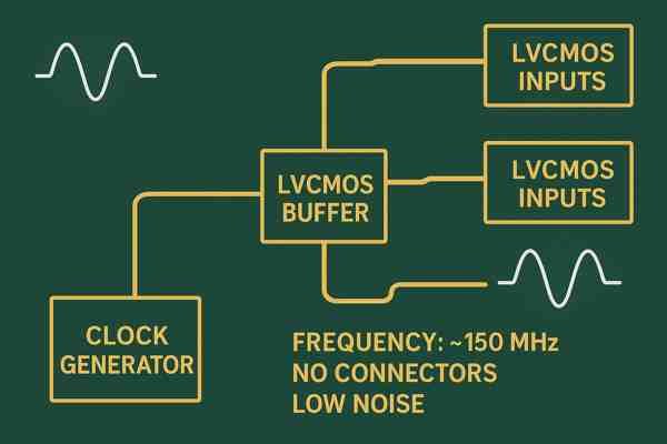
An LVCMOS1 (Low-Voltage Complementary Metal-Oxide-Semiconductor) buffer is the workhorse for general-purpose clock distribution. It’s simple, cheap, and widely available.
Key Characteristics of LVCMOS Buffers
These buffers work with standard logic levels that most digital ICs use. The logic levels are defined by the JEDEC standard JESD8-C.012 and are dependent on the supply voltage (\(V_{CC}\)).
| \(V_{CC}\) | \(V_{IH}\) (min Input High) | \(V_{IL}\) (max Input Low) |
|---|---|---|
| 3.3V | 2.0 V | 0.8 V |
| 2.5V | 1.7 V | 0.7 V |
| 1.8V | \(0.65 \times V_{CC}\) | \(0.35 \times V_{CC}\) |
The Hidden Dangers: Ground Bounce3 and Reflections
The biggest weakness of single-ended signals is their reference to ground. When multiple buffer outputs switch high at the same time, they draw a large, sudden current which can cause the ground level inside the chip to "bounce" upwards. This ground bounce can create significant jitter. It’s also why I avoid them for traces that cross a split in a ground plane or go through a connector, as this creates signal reflections that degrade the clock edge.
This table summarizes the core trade-offs before we dive into the high-speed alternative.
| Feature | Single-Ended (e.g., LVCMOS) | Differential (e.g., LVDS) |
|---|---|---|
| Wiring | 1 wire + Ground reference | 2 complementary wires (\(\text{P/N}\)) |
| Noise Immunity | Low (susceptible to ground noise) | High (common-mode noise rejected) |
| Max Frequency | Lower (\(\approx <200 \text{ MHz}\)) | Much Higher (\(>1 \text{ GHz}\)) |
| Layout Complexity | Simple | Complex (impedance & length matching) |
| Best Use Case | On-board, short distance | Board-to-board, noisy environments |
What Is a Differential Clock Buffer (LVDS, LVPECL, HCSL)?
High-speed designs failing due to clock jitter and EMI? Your single-ended clock might be the culprit, unable to handle the noise and long trace lengths.
A differential clock buffer uses two complementary signals (e.g., \(\text{CLK}^{+}\) and \(\text{CLK}^{-}\)) to distribute a clock. This design provides excellent common-mode noise rejection and supports much higher frequencies (in the Gbps range) and longer distances, making it ideal for noisy environments or board-to-board communication.

Differential signaling4 is my go-to solution for any serious high-performance clocking. The receiver subtracts the two signals, effectively doubling the signal swing and cancelling out any noise that affects both lines equally.
Common Differential Standards and Terminations
The termination scheme is critical and varies by standard.
| Standard | Typical Termination Method | Key Characteristics |
|---|---|---|
| LVDS | Single \(100 \Omega\) resistor across \(\text{P/N}\) lines at the receiver. | Simplest method. Low power. Matches differential impedance. |
| LVPECL | Thevenin or AC-Coupled. E.g., pull-up/pull-down resistors to create a bias voltage and \(100 \Omega\) termination. | More complex, higher power, but very high speed. |
| HCSL | Two \(50 \Omega\) resistors, one from each line (\(\text{P}\) and \(\text{N}\)) to Ground at the receiver. | Standard for PCI Express. Simple but different from LVDS. |
Layout Considerations for Differential Pairs
The physical layout is just as important as the component selection. When I lay out differential pairs, I follow strict rules:
- Controlled Impedance5: I design the traces to have a specific differential impedance, typically \(100 \Omega\) for LVDS/LVPECL or \(85 \Omega\) for HCSL in newer PCIe generations.
- Tight Coupling: The \(\text{P}\) and \(\text{N}\) traces must be routed as close together as the PCB fabrication rules allow.
- Length Matching: The physical lengths of the \(\text{P}\) and \(\text{N}\) traces must be almost identical. For signals \(>1 \text{ Gbps}\), I keep the mismatch below \(5 \text{ mils } (0.127 \text{ mm})\).
What Is a Zero-Delay Buffer (ZDB)?
Trying to sync multiple devices, but the buffer’s own delay is messing up your timing budget? This propagation delay can be a silent killer for system-level synchronization.
A zero-delay buffer (ZDB) uses an internal Phase-Locked Loop (PLL) to actively eliminate the propagation delay between its input clock and its output clocks. This ensures the output signals are phase-aligned with the input, which is critical for large, synchronous systems.
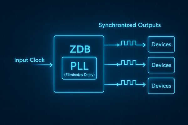
A standard buffer’s propagation delay (\(t_{pd}\)) can be several nanoseconds. A ZDB uses a PLL to compare a feedback output to the input clock and adjusts the phase of all outputs until they match the input perfectly. This table clearly shows the difference.
| Feature | Standard Fan-out Buffer | Zero-Delay Buffer (ZDB) |
|---|---|---|
| Core Technology | Simple logic gates/amplifiers | Phase-Locked Loop (PLL) |
| Propagation Delay6 (\(t_{pd}\)) | Exists (e.g., \(1-2 \text{ ns}\)) and must be budgeted | Effectively zero (phase-aligned outputs) |
| Jitter Performance | Adds low jitter | Can add PLL jitter, but can also "clean" a noisy input |
| Complexity | Low | High (requires lock time, careful bypassing) |
| Cost | Low | Higher |
| Best Use Case | Simple fan-out where delay is acceptable | Synchronous systems needing phase alignment |
ZDBs vs. Clock Synthesizers
It’s important not to confuse a ZDB with a clock synthesizer. A ZDB primarily distributes and phase-aligns an existing clock. A clock synthesizer creates new clock frequencies, often using more complex PLLs to multiply a crystal reference frequency.
What Are the Most Important Specifications in a Clock Buffer Datasheet?
Choosing a clock buffer feels like a lottery? Picking the wrong part based on a single spec can lead to subtle timing failures that are a nightmare to debug.
The most critical specs are additive jitter (the noise the buffer adds), propagation delay, and output-to-output skew (the timing difference between outputs). These directly impact signal integrity and the system’s timing budget. Power supply rejection is also crucial.
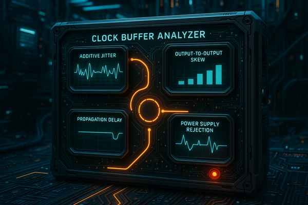
When I open a datasheet, I look for more than just the basics. The real story is in the performance metrics.
Key Performance Specifications
| Specification | What It Means | A "Good" Value (Example) |
|---|---|---|
| Additive Jitter | Noise added by the buffer. This is a critical part of your jitter budget. | \(< 50 \text{ fs RMS}\) (For PCIe Gen 4/5) |
| Output-to-Output Skew | The maximum time difference between the fastest and slowest outputs. | \(< 35 \text{ ps}\) (For DDR4 memory) |
| PSRR (Power Supply Rejection Ratio)7 | The buffer’s ability to reject noise from its own power supply. | \(> -50 \text{ dB @ } 10 \text{ MHz}\) |
| Propagation Delay (\(t_{pd}\)) | The time it takes for the signal to travel from input to output. | \(\approx 1.5 \text{ ns}\) (For a simple fanout buffer) |
PSRR is a spec I never ignore. Noise on the buffer’s \(V_{CC}\) pin can directly translate into jitter on the clock outputs. A buffer with a high \(\text{PSRR}\) is more immune to a noisy power rail.
How Is the Right Clock Buffer Chosen for a Design?
Overwhelmed by thousands of clock buffer options? Making the wrong choice can mean a costly board respin or, worse, a product that fails in the field.
Choose a clock buffer by first defining your system’s needs: required frequency, number of outputs, and logic levels. Then, analyze your timing budget to determine the maximum acceptable jitter, propagation delay, and skew. Finally, simulate and select the most cost-effective option.

I use a structured approach to make sure the component I choose is the right fit. It starts with filling out a checklist like this for my project.
Clock Buffer Selection Checklist
| Parameter | My Requirement | Notes |
|---|---|---|
| Input Clock Frequency | ______ \(\text{MHz/GHz}\) | What is the clock speed? |
| Number of Outputs | ______ | Always add 1-2 spares for testing. |
| Input Logic Level | LVCMOS / LVDS / etc. | E.g., 1.8V LVCMOS from FPGA. |
| Output Logic Level(s) | LVCMOS / HCSL / etc. | Can be multiple types on one chip. |
| Max Additive Jitter | \(< \text{ \_\_\_\_\_\_ fs/ps RMS}\) | Calculated from the system jitter budget. |
| Max Output-Output Skew | \(< \text{ \_\_\_\_\_\_ ps}\) | Critical for parallel buses like memory. |
| Zero-Delay Needed? | Yes / No | Is phase alignment with the input critical? |
| Package & Power | ______ / ______ \(\text{V}\) | What footprint and \(V_{CC}\) do I have available? |
Analyze, Simulate, and Select
With this checklist filled out, I analyze my timing budget. For a high-speed interface, I download the IBIS model8 for my top candidates. This lets me simulate the buffer’s performance in my specific PCB layout before I build hardware, which has saved me from countless potential issues.
Conclusion
Clock buffers are essential for reliable timing. Choosing the right one—single-ended, differential, or zero-delay—depends entirely on your system’s speed, noise, and synchronization needs.
-
Explore the benefits of LVCMOS technology in clock distribution, including its cost-effectiveness and simplicity. ↩
-
Learn the official voltage thresholds and logic level definitions for LVCMOS devices directly from the JEDEC JESD8-C.01 standard. ↩
-
Learn about ground bounce and its impact on digital circuits, crucial for understanding signal integrity. ↩
-
Understanding differential signaling can enhance your knowledge of high-performance clocking and noise cancellation. ↩
-
Understanding controlled impedance is crucial for ensuring signal integrity in high-speed PCB layouts, especially for differential signaling applications. ↩
-
Exploring propagation delay helps in grasping its impact on circuit performance and design considerations. ↩
-
Understanding PSRR is crucial for designing reliable circuits, as it impacts noise immunity and overall performance. ↩
-
Understanding the IBIS model is crucial for simulating buffer performance, ensuring your design meets timing requirements. ↩


