Struggling to pass EMC testing? Your Ethernet port is failing radiated emissions, and you can't figure out why. The problem might be the humble Ethernet cable itself, acting as an unintended antenna.
Yes, Ethernet cables are a primary source of EMI. Imbalances in the circuit create common-mode currents that flow along the length of the cable. This turns the entire cable into an efficient antenna, radiating noise that causes failures in EMC compliance testing, especially above 30 MHz.
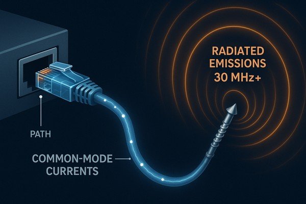
I've been there more times than I can count. You're in a shielded room, the clock is ticking, and the spectrum analyzer1 shows a massive spike that violates the CISPR 322 limit line. You trace it right back to the Ethernet cable. It’s a frustratingly common problem, but it's one that is entirely fixable with disciplined engineering. The key is understanding that the cable isn't the source of the noise, but the vehicle for it. The real problem starts on your PCB. Let's break down why this happens and, more importantly, how to design a bulletproof Ethernet interface from the ground up.
What causes common-mode noise on Ethernet cables?
Your differential signals look clean on the scope, but radiated emissions are still high. You're chasing layout ghosts, unsure what's causing the problem. The issue is almost always common-mode noise generated from simple, easy-to-miss design imbalances.
Common-mode noise on Ethernet cables is caused by asymmetry. This includes mismatched trace lengths, impedance discontinuities from vias, unequal coupling to ground, and return path interruptions. These imbalances convert a portion of the desired differential signal into unwanted common-mode current, which radiates from the cable.
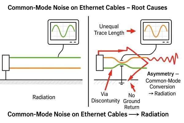
In my experience, the root cause of common-mode conversion is always a disruption of the electromagnetic field symmetry. An ideal differential pair has two signals whose fields are perfectly equal and opposite, resulting in zero net radiation. Any physical or electrical asymmetry, no matter how small, breaks this cancellation. This asymmetry can arise from several sources on your PCB.
How Physical Layout Asymmetry Creates Noise
This is the most common culprit. It includes mismatched trace lengths, which create a phase difference, and inconsistent spacing, which causes impedance variations. Even using a via on one trace of a pair but not the other introduces a significant delay and impedance mismatch. The rule is to treat the differential pair as a single, symmetrical entity throughout its entire path.
How Return Path Discontinuities3 Create Noise
This is a more subtle but equally critical issue. Every signal has a return current that flows in the reference plane directly beneath it. If you route a differential pair over a split or gap in that ground plane, the return current is forced to make a huge detour. This large current loop is an incredibly efficient antenna and a major source of common-mode noise.
| Source of Asymmetry | Impact on Signal | Recommended Design Rule / Mitigation |
|---|---|---|
| Trace Length Mismatch | Creates a phase difference between the pair's signals. | Match lengths to < 25 mils (0.635 mm) for 100BASE-TX; < 5 mils (0.127 mm) for Gigabit. |
| Via Asymmetry | Introduces impedance and delay mismatch. | If one trace uses a via, the other must have a matching one. Add 2+ ground stitching vias per signal via. |
| Return Path Discontinuity | Forces return current into a large, radiating loop. | Never route pairs over splits in the ground plane. Maintain a solid reference plane. |
| Component Tolerance | Creates imbalance in termination circuits. | Use 1% or better tolerance resistors for all termination and biasing networks. |
What are the most common Ethernet radiated emissions failure frequencies?
You see a sharp spike at 125 MHz during your EMC scan. You're not sure if it's from your Ethernet port or another part of the system. The good news is that Ethernet EMI leaves a very distinct fingerprint.
For 100BASE-TX Ethernet, the most common failure frequencies are odd harmonics of the 25 MHz clock, especially 75 MHz (3rd), 125 MHz (5th), and 175 MHz (7th). For 1000BASE-T (Gigabit), which has a 62.5 MHz fundamental rate, failures often occur at 125 MHz and 187.5 MHz.
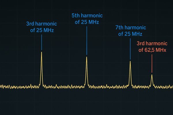
These frequencies are direct signatures of the Ethernet PHY's operation and clocking schemes. Understanding them allows you to immediately identify the Ethernet port as a likely culprit during EMC testing.
Common Failure Frequencies for 100BASE-TX
Fast Ethernet uses a 25 MHz clock. While its MLT-3 data encoding concentrates the desired signal energy below 40 MHz, any common-mode conversion will efficiently generate sharp, powerful harmonics. The 5th harmonic at 125 MHz is often the worst offender because a standard 1-meter Ethernet cable is a nearly perfect half-wavelength dipole antenna4 at this frequency, making it an incredibly efficient radiator.
Common Failure Frequencies for 1000BASE-T
Gigabit Ethernet uses a 62.5 MHz symbol rate with PAM-5 encoding across all four pairs. This complexity means more opportunities for imbalance. The most common failure points I see are at the 2nd harmonic (125 MHz) and 3rd harmonic (187.5 MHz).
| Ethernet Standard | Fundamental Rate | Common Failure Frequencies (Radiated Emissions) |
|---|---|---|
| 100BASE-TX | 25 MHz | 75 MHz, 125 MHz, 175 MHz |
| 1000BASE-T | 62.5 MHz | 125 MHz, 187.5 MHz, 312.5 MHz |
How to debug EMI from an Ethernet port?
Your product has failed its radiated emissions test. The test lab bill is climbing, and you're stuck in an expensive loop of tweaking the design and re-testing. A systematic debugging approach can find the root cause quickly and efficiently.
Start by using a near-field probe with a spectrum analyzer to find the loudest part—the cable, the connector, or the PHY. Then, use a current clamp on the Ethernet cable to measure common-mode current. Systematically disconnecting the cable is the definitive test to confirm it's the source.
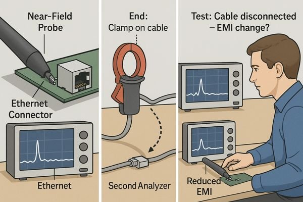
When I'm in the lab, I work from a pre-prepared "EMC debug kit" and document every single step. Guesswork is expensive; data is cheap. The process involves systematically isolating the problem from the system level down to the component level.
Debug Step 1: Isolate the Radiating Element
The first question is always: "Is the cable the antenna?" The simplest way to test this is to measure the emission with the Ethernet cable connected, and then measure it again with the cable unplugged. A drop of more than 10 dB in the problem frequency's amplitude is a clear confirmation that the cable is radiating the common-mode noise.
Debug Step 2: Quantify and Localize the Noise
Once the cable is confirmed as the radiator, use an RF current clamp to measure the magnitude of the common-mode current. This gives you a baseline for any fixes. A reading above 5 µA is a red flag for CISPR 32 Class B. Next, use a small H-field (magnetic) probe to sniff the PCB itself. This will help you pinpoint the physical location on the board where the noise is strongest, often revealing a flawed trace, a bad ground connection, or a noisy component.
| Step | Action | Expected Outcome / Observation |
|---|---|---|
| 1 | Confirm the Radiator With the system running, disconnect the Ethernet cable. | If the emission peak drops by >10 dB, the cable is the primary radiator. You're chasing a common-mode current problem. |
| 2 | Quantify the Current Reconnect the cable. Place an RF current clamp around it. | Measure the common-mode current at the failure frequency. A reading >5 µA is a likely cause for a CISPR 32 Class B failure. |
| 3 | Localize the Source Use a small H-field (magnetic) probe to scan the PCB layout. | The "hot spot" on the spectrum analyzer will identify the physical source of the noise (e.g., PHY-magnetics traces, bad ground). |
| 4 | Test Live Fixes Snap a ferrite bead on the cable. Use copper tape for temporary grounding. | If a ferrite helps, a board-level CMC will likely work. If the tape helps, your grounding scheme is flawed. |
What are the PCB layout best practices for an Ethernet PHY and magnetics?
You're starting a new design and want to avoid Ethernet EMI problems from the beginning. You know the layout is critical, but you're not sure about the specific rules. Getting the layout right is the single most effective way to ensure EMC compliance.
Place the magnetics as close to the RJ45 connector as possible. Keep traces between the PHY and magnetics short, symmetrical, and impedance-controlled to 100Ω. Most importantly, create an isolated ground "moat" under the magnetics and connector, and ensure this doesn't compromise the board's mechanical integrity.
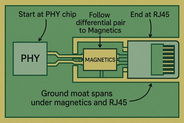
A good layout is about fanatical attention to detail. It's the cheapest form of EMI control and revolves around two core principles: maintaining signal path symmetry and providing a clean ground/isolation strategy.
Layout Practice: The Isolation "Moat" and Grounding Strategy
The most critical layout feature is the isolation gap, or "moat," that separates the PCB's digital ground from the connector's chassis ground. You must cut away all copper planes under the magnetics and the RJ45 connector area. I use a minimum gap of 100 mils (2.54 mm). For medical devices (IEC 60601-15), this can increase to 8mm or more. No signal or power traces should ever cross this moat; only the Ethernet signal pairs are allowed.
Layout Practice: Symmetrical Routing for High-Speed Pairs
The traces between the PHY and magnetics are a high-speed differential interface. They must be routed as a perfectly coupled pair with matched lengths and controlled 100Ω differential impedance. Keep them as short as possible, ideally under one inch. Every via adds discontinuity, so if one trace needs a via, the other must get one too. Always place at least two ground stitching vias next to any signal vias to provide a continuous return path for the current.
How to properly ground the shield of an RJ45 connector to the chassis?
You have a shielded RJ45 connector and a metal enclosure. You're wondering how to connect the connector's metal shell to the chassis. A poor shield connection can make your EMI problems worse, not better.
The shield of the RJ45 connector must be connected directly to the chassis ground using multiple, low-inductance paths. This chassis ground must be separate from your PCB's digital ground. Use connector mounting screws or a conductive gasket for the best connection.
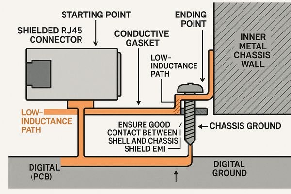
The goal is to create a 360-degree, low-impedance bond between the cable shield and the product's metal chassis. This bond acts as a highway for high-frequency noise to be shunted safely to the chassis ground, away from your sensitive electronics.
Grounding Method 1: Direct Mechanical Bond to Chassis
This is the gold standard for performance. It involves using a connector with metal mounting flanges that screw directly into the product's chassis. This provides the lowest possible inductance path. For best results, I specify star washers under the screw heads to ensure they cut through any paint or anodization on the chassis, creating a reliable, long-term metal-to-metal connection.
Grounding Method 2: Isolated RC Ground for Safety
In applications where DC isolation between the circuit and chassis is required for safety (per standards like IEC 62368-16), a direct bond is not allowed. In this case, the shield is connected to the chassis ground via a parallel resistor-capacitor network. A 1MΩ resistor provides a DC path for fault currents, while a high-voltage 2kV-rated, 1nF-4.7nF capacitor provides the essential low-impedance path for high-frequency EMI noise.
| Grounding Method | Best For | Pros | Cons | Implementation Key |
|---|---|---|---|---|
| Direct Mechanical Bond | Products with a metal chassis; maximum EMI performance. | Lowest possible inductance; most effective EMI shield. | Creates a DC path between circuit and chassis. | Use multiple screws with star washers to ensure a tight metal-to-metal bond. |
| RC Safety Ground | Products requiring DC isolation for safety (e.g., IEC 62368-1). | Provides DC isolation; blocks ground loops. | Higher inductance than a direct bond; less effective for EMI. | Use a 1MΩ resistor in parallel with a 2kV-rated, 1nF-4.7nF ceramic capacitor. |
How does the "Bob Smith" termination reduce Ethernet emissions?
You’ve heard engineers talk about the "Bob Smith" termination as a fix for Ethernet EMI. You understand it involves resistors and a capacitor, but you’re not sure how it actually works or when to use it.
The Bob Smith termination reduces common-mode emissions by providing a low-impedance path for common-mode currents to return to ground before they can flow onto the Ethernet cable. It consists of a 75Ω resistor from each transformer center tap to a central point, which is then connected to ground via a capacitor.
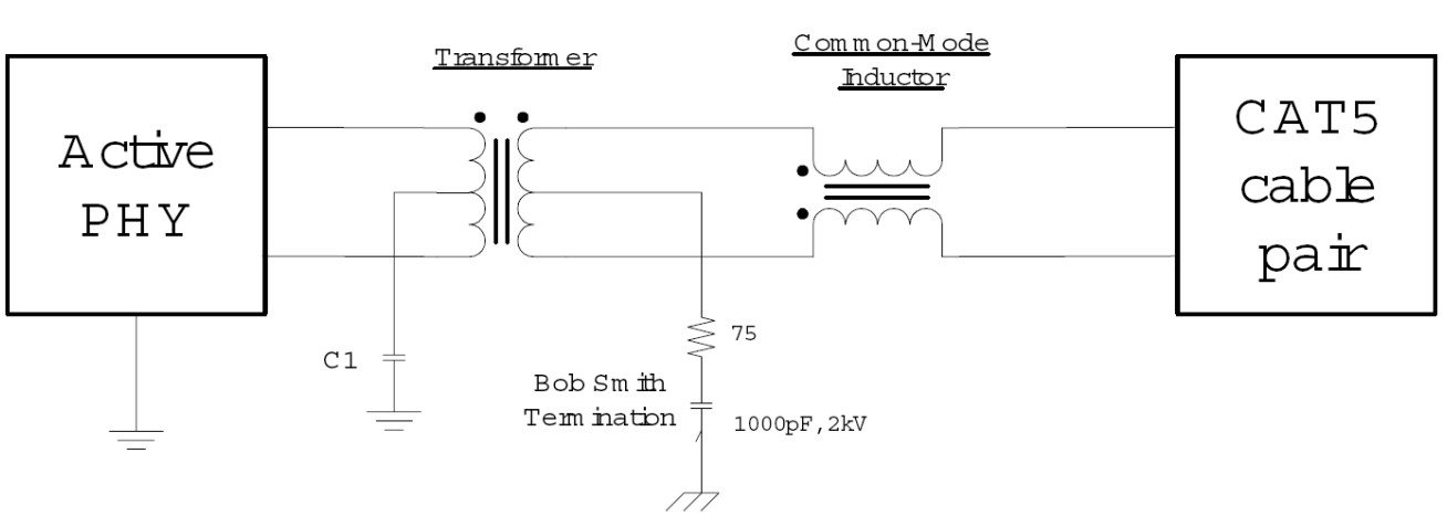
This is a classic EMC fix, but I view it as a patch, not a primary design choice. If your layout is good, you shouldn't need it. I often include the footprint for it, but leave it unpopulated as a "Plan B" for EMC testing.
How the Bob Smith Termination Circuit Works
The cable side of the Ethernet magnetics includes a center tap for each differential pair. The Bob Smith termination connects these center taps together through 75Ω resistors. This common point is then tied to the chassis ground through a high-voltage capacitor. This network provides a path to ground that matches the common-mode impedance of the cable, effectively absorbing common-mode currents before they can radiate from the cable.
Performance Trade-Offs of the Bob Smith Termination
This fix is not free. In my lab measurements, adding a Bob Smith termination typically increases the insertion loss7 of the signal path by 0.1 to 0.2 dB. This may seem insignificant, but for a system that needs to support a full 100-meter cable run, that extra loss can be the difference between a pass and a fail on the network signal integrity compliance test suite.
| Component | Value/Type | Purpose |
|---|---|---|
| Resistors (R) | 75Ω, 1% tolerance | Provides impedance matching for common-mode current. |
| Capacitor (C) | 1nF - 4.7nF, 2kV, X7R/C0G ceramic | Shunts high-frequency noise to chassis ground. |
| Connection Point | Chassis Ground (on the connector side of the moat) | Dumps the noise to the main system shield/earth. |
When and where should a common-mode choke be used on an Ethernet interface?
You're trying to decide if you need a common-mode choke (CMC) for your Ethernet design. You see them on some reference designs but not others, and you're unsure of the trade-offs.
A common-mode choke should be used when you need maximum suppression of common-mode noise, especially in designs that must pass stringent EMC standards like CISPR 32 Class B. It should be placed on the PCB between the Ethernet PHY and the magnetics.
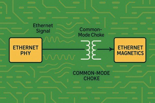
For any high-reliability product, I consider a CMC to be a mandatory part of the design. The cost of the component is trivial compared to the cost of a failed compliance test. Adding a good choke can provide 6 to 15 dB of emission reduction at a problem frequency.
How a Common-Mode Choke Filters Noise
A CMC is a differential filter. It presents a very low impedance to your differential Ethernet signal, allowing it to pass through unaffected. However, for common-mode noise (where currents on both lines flow in the same direction), the choke presents a very high impedance, effectively blocking the noise from propagating down the line.
Advanced Criteria for Selecting a Common-Mode Choke
Choosing the right choke is critical. You must look beyond the basic current rating and check the impedance-versus-frequency curves in the datasheet. A common mistake is choosing a choke that has high impedance at the wrong frequency. For PoE (Power-over-Ethernet) applications, you must also select a choke that will not saturate under the DC bias current, as saturation will cause its impedance to collapse, rendering it useless.
| CMC Selection Parameter | What to Look For in the Datasheet | Reason |
|---|---|---|
| Common-Mode Impedance | >1500Ω from 50 MHz to 200 MHz | Provides high impedance to block the unwanted common-mode noise. |
| Differential-Mode Impedance | < 5Ω across the 1-100 MHz signal band | Ensures the choke does not degrade the Ethernet signal itself. |
| Rated Current | Must be higher than the max PoE current (e.g., >1A for PoE++). | Prevents the ferrite core from saturating, which would make it ineffective. |
| Self-Resonant Frequency (SRF)8 | Should be well above 100 MHz. | Above the SRF, the choke acts like a capacitor and loses its effectiveness. |
How to select integrated magnetics (a "magjack") for the best EMC performance?
You're selecting the RJ45 connector for your design and see options for simple connectors or integrated magnetics, often called "magjacks." You're wondering if a magjack can help with EMC and how to choose the best one.
A high-quality magjack can significantly improve EMC performance. Select a magjack with built-in common-mode chokes and a high, flat common-mode rejection ratio (CMRR). Crucially, source these components from authorized distributors to avoid counterfeit parts.
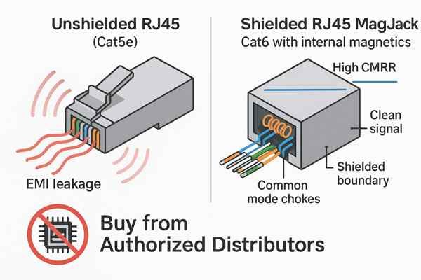
I almost exclusively use magjacks in new designs. However, this is one area where I've been burned by supply chain issues and counterfeit components.
The Danger of Counterfeit Magjacks
I once worked on a project where a production batch was failing EMC catastrophically. The design hadn't changed, but the magjacks had been sourced from a new, cheaper supplier to save cost. After decapping the components, we found they were counterfeits with poorly wound, unbalanced transformers inside. They looked identical on the outside. The lesson was expensive but clear: Always source critical performance components like magnetics from fully authorized, traceable distributors.
How to Read a Magjack Datasheet for EMC Performance
Don't just look at the front page specifications. You must analyze the performance graphs. A good magjack will have a Common-Mode Rejection Ratio (CMRR)9 that is very low (e.g., -40 dB) and remains flat across the entire frequency band. A curve that slopes upward at high frequencies indicates a poorly designed part that will fail you where you need it most. Also, check the schematic within the datasheet to confirm it includes the integrated common-mode chokes that are critical for EMI suppression.
What is the difference in EMC performance between shielded (STP) and unshielded (UTP) cables for a product?
You're deciding whether to specify shielded (STP) or unshielded (UTP) cable for your product. UTP is cheaper and more common, but you're concerned about passing EMC. You need to know if the extra cost of STP is justified.
A properly terminated Shielded Twisted Pair (STP) cable offers vastly superior EMC performance compared to UTP. The shield contains radiated emissions and protects against external noise, but only if it's connected to chassis ground at both ends.
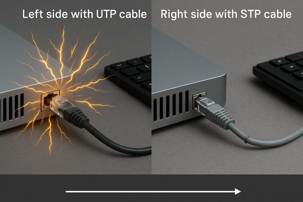
| Feature | Unshielded Twisted Pair (UTP) | Shielded Twisted Pair (STP) |
|---|---|---|
| Cost | Lower | Higher |
| EMC Emissions | Fair to Poor | Excellent |
| EMC Immunity | Fair to Poor | Excellent |
| Best Environment | Office, Home (Low Noise) | Industrial, Medical, Automotive (High Noise) |
| Key Dependency | Performance relies entirely on the perfection of your PCB layout. | Performance relies entirely on a proper 360° shield termination at both ends. |
System-Level Considerations for Choosing STP vs. UTP
The choice is a system-level risk assessment. For a cost-sensitive consumer product used in a home, UTP is often acceptable. For an industrial controller used in a factory full of VFD motors, STP is mandatory for reliable operation.
The User Factor: Documenting Cable Requirements
Here's a hard-won piece of advice: Specify the required cable type in your user manual. I've debugged field issues where a customer's system was unreliable because they used a cheap UTP cable in a noisy factory, even though our device was designed and tested with STP. Your design's performance is only as good as the weakest link, which is often the cable the user chooses.
How to pass Ethernet surge immunity tests?
Your product is being tested for surge immunity according to IEC 61000-4-5. The high-voltage pulses are causing your Ethernet port to reset or fail. You need a robust protection strategy.
To pass Ethernet surge tests, use a combination of high-voltage isolation magnetics (≥2.25kV), a low-inductance chassis ground path, and a low-capacitance Transient Voltage Suppression (TVS) diode array placed on the cable side of the magnetics.
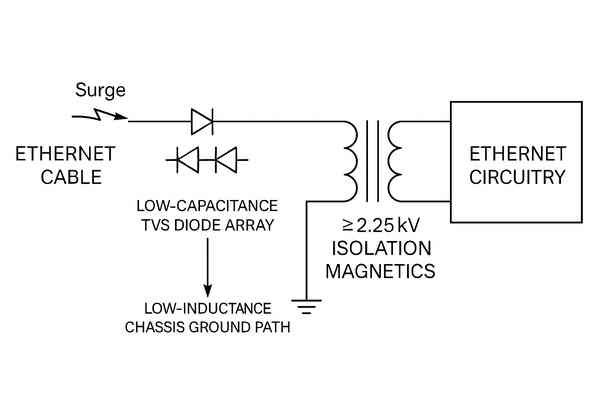
Surge immunity is about diverting massive amounts of energy. Your protection circuit must create a path to ground that is so much more attractive to the surge pulse than the path through your sensitive electronics.
A Layered Defense Strategy for Surge Protection
I think of surge protection in three layers:
- The Wall (Isolation): Your primary defense is the isolation voltage of the magnetics. Standard 1.5kV parts are often insufficient for industrial gear. I use 2.25kV as a baseline and go up to 4kV or 6kV for anything connected to outdoor cabling.
- The Diverter (TVS Diodes): The TVS array is the active component that shunts the surge current to ground. Its placement is critical: it must be the very first thing the signal sees after the connector, before the magnetics.
- The Sink (Grounding): The layout of the TVS diode's path to the chassis ground is paramount. Use wide, short polygon pours, not thin traces. Every nanohenry of inductance in this path develops a voltage (V = L * di/dt) that works against your protection scheme.
| Protection Component | Key Specification | Layout Criticality |
|---|---|---|
| Ethernet Magnetics | Isolation Voltage: ≥ 2.25kV (Hi-Pot) | Forms the primary voltage isolation barrier (the "wall"). |
| TVS Diode Array | Low Capacitance: < 2.5 pF, Low Clamping Voltage | Must be on the cable side. Path from TVS to ground must be a low-inductance pour. |
| Chassis Ground Plane | Low Impedance / Low Inductance | Must be robustly tied to the main product chassis/earth to safely sink the energy. |
How to pass Ethernet Electrical Fast Transient (EFT) immunity tests?
Your device resets during EFT testing and you're failing immunity. You can't figure out how the high-frequency noise is getting into your system and causing data errors or lockups. A multi-layered defense is key.
Passing EFT requires a multi-pronged defense: a solid shield-to-chassis ground, a common-mode choke to filter burst noise, and meticulous power supply filtering for the Ethernet PHY using a well-placed PI filter.
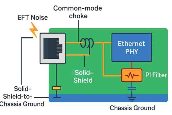
EFT is a high-frequency noise assault. Unlike surge, which is about high energy, EFT is about high frequency and fast rise times. The noise couples into your system through parasitic capacitance, so your defense must be based on high-frequency filtering principles.
Using a PI Filter10 to Protect the PHY from EFT
The most critical part of this defense is isolating the Ethernet PHY's power supply from system-level noise. You must create a proper PI filter on the PCB.
- First Capacitor: Place a
0.1µFcapacitor where the main power rail enters the Ethernet section of your layout. - Series Inductor: After this capacitor, place a high-frequency ferrite bead (like a Murata BLM series) on the power trace leading to the PHY. This is the series element that blocks high-frequency noise.
- Second Capacitor: Immediately at the PHY's power pin(s), place another set of decoupling capacitors (e.g.,
10nFand1nF).
This Capacitor-Inductor-Capacitor structure creates a very effective low-pass filter, ensuring the PHY has a clean, stable power source even during an EFT event. Placing these components out of order will render the filter ineffective.
Conclusion
Ethernet EMI is a solvable, physics-based problem. It demands fanatical attention to detail in your layout, a deep understanding of grounding, and a multi-layered strategy for filtering and protection. Master these fundamentals, and you can turn one of the most common sources of EMC failure into a robust and reliable part of your design.
-
Learn how a spectrum analyzer helps identify electromagnetic interference sources, crucial for troubleshooting and compliance in electronics design. ↩
-
Understanding CISPR 32 is crucial for ensuring compliance in Ethernet designs, helping you avoid costly redesigns and failures. ↩
-
Learning about return path discontinuities can help you avoid common pitfalls in PCB layout. ↩
-
Learn how a half-wavelength dipole antenna operates to understand why Ethernet cables can radiate efficiently at certain frequencies during EMC testing. ↩
-
Learn how IEC 60601-1 safety standards impact PCB design, especially isolation requirements, to ensure compliance and patient safety in medical devices. ↩
-
Delve into IEC 62368-1 standards to ensure your products meet safety regulations in electronics. ↩
-
Learn about insertion loss and its impact on network performance, crucial for ensuring compliance in long cable runs. ↩
-
Understanding SRF is essential for selecting the right choke to ensure optimal performance in your designs. ↩
-
Exploring CMRR's impact on EMC performance will enhance your knowledge of selecting reliable components. ↩
-
Understanding PI Filters is crucial for effective noise management in electronic designs, especially against EFT. ↩


