
Are you pushing the density limits on your PCB design? Choosing a via size that’s too small can lead to costly manufacturing failures. Let’s look at what fabricators can actually deliver reliably.
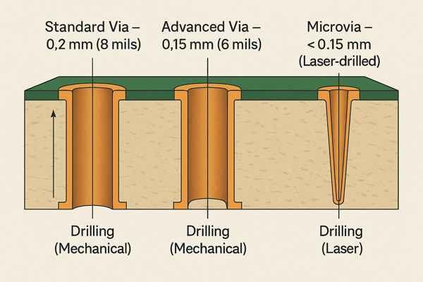
Most PCB fabricators can reliably produce vias with a mechanical drill size of 0.2 \(\text{mm}\) (about 8 \(\text{mils}\)). Advanced fabricators can push this to 0.15 \(\text{mm}\) (6 \(\text{mils}\)). Anything smaller typically requires more expensive laser-drilled microvias, which are in a different class of manufacturing.
Choosing the right via size isn’t just about what’s physically possible. It’s a critical engineering trade-off between board density, signal integrity, power delivery, and, most importantly, manufacturing cost and reliability. In my nearly 20 years as a hardware engineer, I’ve seen countless projects get delayed or go over budget because of aggressive via choices that weren’t truly necessary. The key is to understand the different thresholds where cost and risk start to climb. We will explore not only the standard choices but also the advanced techniques and trade-offs that separate a good design from a great one.
What is a standard, cost-effective via size for a typical PCB?
Struggling to keep your prototype costs down? 😟 Your choice of via size could be the culprit, adding hidden expenses without you realizing it. Let’s define the sweet spot for cost and manufacturability.
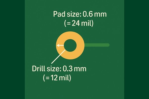
For maximum cost-effectiveness, the industry standard via uses a 0.3 \(\text{mm}\) (\(\approx\)12 \(\text{mil}\)) drill with a 0.6 \(\text{mm}\) (\(\approx\)24 \(\text{mil}\)) pad. This combination is robust, supported by virtually all manufacturers at their lowest price tier, and offers excellent production yield.
Understanding Cost Tiers for PCB Vias
The 0.3 \(\text{mm}\) drill / 0.6 \(\text{mm}\) pad via is the industry workhorse for a reason. A key factor behind this dimension is the drill-to-copper clearance rule. Most fabricators require a minimum clearance of 0.2 \(\text{mm}\) (8 \(\text{mils}\)) from the edge of a drilled hole to any adjacent copper feature. This clearance rule, more than any other, often dictates your maximum routing density.
Here is a breakdown of how via sizes typically map to cost.
| Cost Tier | Drill Size | Pad Size | Relative Cost Index 💰 | Use Case |
|---|---|---|---|---|
| Standard | \(\geq\) 0.3 \(\text{mm}\) (12 \(\text{mil}\)) | \(\geq\) 0.6 \(\text{mm}\) (24 \(\text{mil}\)) | 1x | General purpose, non-dense areas |
| Advanced | 0.2 \(\text{mm}\) (8 \(\text{mil}\)) | 0.45 \(\text{mm}\) (18 \(\text{mil}\)) | 1.5x – 2x | Denser routing, some BGA breakouts |
| Leading-Edge | 0.15 \(\text{mm}\) (6 \(\text{mil}\)) | 0.40 \(\text{mm}\) (16 \(\text{mil}\)) | >3x | High-density, fine-pitch components |
What is the difference between the drill size and the finished hole size for a via?
Have you ever specified a via hole size in your design, only to find the physical hole on the finished board is smaller? This common confusion can cause problems. It’s crucial to understand the manufacturing step that causes this difference.
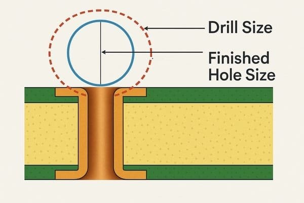
The drill size is the diameter of the physical bit that creates the hole in the laminate. The finished hole size is the diameter that remains after the hole is plated with copper. The finished hole is always smaller than the initial drill size.
The Role of Copper Plating in Determining Finished Via Size
The reduction in hole size is directly related to the plating thickness, which is influenced by your specified copper weight. For a high-power board with 2\(\text{oz}\) (70\(\mu\text{m}\)) finished copper, the plating in the barrel will be significantly thicker than on a standard 1\(\text{oz}\) (35\(\mu\text{m}\)) board. This means the fabricator needs a larger drill bit to achieve the same finished hole size.
The table below illustrates this critical relationship.
| Target Finished Hole | Plating Thickness (1\(\text{oz}\) Cu) | Required Drill (1\(\text{oz}\) Cu) | Plating Thickness (2\(\text{oz}\) Cu) | Required Drill (2\(\text{oz}\) Cu) |
|---|---|---|---|---|
| 0.20 \(\text{mm}\) (8 \(\text{mil}\)) | \(\approx\)25 \(\mu\text{m}\) | 0.25 \(\text{mm}\) | \(\approx\)50 \(\mu\text{m}\) | 0.30 \(\text{mm}\) |
| 0.30 \(\text{mm}\) (12 \(\text{mil}\)) | \(\approx\)25 \(\mu\text{m}\) | 0.35 \(\text{mm}\) | \(\approx\)50 \(\mu\text{m}\) | 0.40 \(\text{mm}\) |
| 0.40 \(\text{mm}\) (16 \(\text{mil}\)) | \(\approx\)25 \(\mu\text{m}\) | 0.45 \(\text{mm}\) | \(\approx\)50 \(\mu\text{m}\) | 0.50 \(\text{mm}\) |
What is the minimum required annular ring size for a via?
Ever get back a batch of prototype boards where some vias are breaking out of their copper pads? 😱 This is called a "tangency" or "breakout" and it can create an open circuit. It’s caused by an insufficient annular ring.
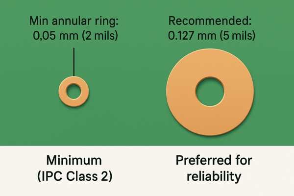
The absolute minimum annular ring for a standard commercial product (IPC-A-600 Class 2) is 0.05 \(\text{mm}\) (\(\approx\)2 \(\text{mils}\)). However, to ensure good yield and reliability, I strongly recommend designing with a minimum annular ring of 0.127 \(\text{mm}\) (5 \(\text{mils}\)) whenever possible.
Why the Annular Ring is Your Manufacturing Safety Margin
The annular ring is your guard band against misregistration during PCB fabrication. Its size is calculated as:
\(\text{Annular Ring} = \frac{(\text{Pad Diameter} – \text{Finished Hole Diameter})}{2}\)
The IPC defines specific requirements based on the product’s intended reliability, which are crucial to understand.
| IPC Class | Description | Annular Ring Requirement | Allowed Breakout Condition |
|---|---|---|---|
| Class 1 | General Electronic Products | Not explicitly defined; relies on minimum land. | 90\(^\circ\) breakout is permitted. |
| Class 2 | Dedicated Service Electronics | 0.05 \(\text{mm}\) (2 \(\text{mil}\)) minimum (internal & external). | 90\(^\circ\) breakout is permitted, but undesirable. |
| Class 3 | High Reliability / Aerospace | 0.05 \(\text{mm}\) (2 \(\text{mil}\)) minimum, with no breakout allowed on internal layers. | Not permitted. |
For any design pushing the limits, I enable teardrops1 in my EDA tool. This adds a copper fillet where a trace joins a pad, reinforcing the connection and providing cheap insurance against breakout.
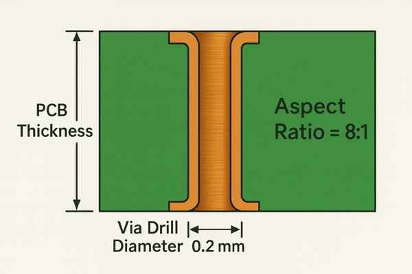
What is the aspect ratio of a PCB via and why does it matter?
Have you ever designed a thick board with very small vias, only to be told by the fabricator that it’s not manufacturable? The problem is likely the via’s aspect ratio. This is a critical constraint that limits how small your vias can be.
The aspect ratio is the ratio of the PCB’s total thickness to the via’s drill diameter. Most fabricators can reliably achieve an 8:1 aspect ratio using standard processes. Advanced fabricators might offer 10:1 or 12:1, but at a significantly higher cost and risk.
Via Aspect Ratio: A Critical Manufacturing Limit
Achieving uniform plating in a deep, narrow hole is a major chemical challenge. To overcome this, fabs use advanced plating technologies.
| PCB Thickness | Smallest Drill Size | Resulting Aspect Ratio | Risk Level | Plating Technology Recommendation |
|---|---|---|---|---|
| 1.6 \(\text{mm}\) | 0.20 \(\text{mm}\) | 8:1 | Standard ✅ | Standard DC Plating |
| 1.6 \(\text{mm}\) | 0.16 \(\text{mm}\) | 10:1 | Advanced ⚠️ | Pulse Plating2 |
| 2.4 \(\text{mm}\) | 0.30 \(\text{mm}\) | 8:1 | Standard ✅ | Standard DC Plating |
| 2.4 \(\text{mm}\) | 0.24 \(\text{mm}\) | 10:1 | Advanced ⚠️ | Pulse Plating |
| 2.4 \(\text{mm}\) | 0.20 \(\text{mm}\) | 12:1 | Leading-Edge 🚨 | Advanced Pulse / Via-Fill Required |
Pulse plating uses a complex electrical waveform to deposit copper more evenly in deep holes, enabling reliable manufacturing at higher aspect ratios.
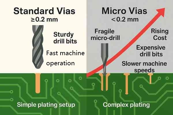
How does via size affect PCB manufacturing cost?
You’ve finished a dense layout using tiny 0.15 \(\text{mm}\) vias, and the prototype quote comes back 3x higher than expected. What happened? 💸 The via size itself is a primary driver of PCB fabrication cost.
Cost rises sharply when you use a drill size smaller than 0.2 \(\text{mm}\) (8 \(\text{mils}\)). Smaller vias require more expensive, fragile drill bits, slower machine speeds, and more complex plating processes. These factors combine to increase both the time and risk of manufacturing.
Key Cost Drivers for Manufacturing PCB Vias
The total cost impact is a combination of several factors, some of which are not obvious.
| Cost Driver | Why it Increases Cost with Smaller Vias | Impact |
|---|---|---|
| Tooling (Drill Bits)3 | Smaller bits are more expensive and have a shorter lifespan. | Moderate |
| Machine Time | Slower ‘peck drilling’ is required to prevent breakage. | High |
| Plating Process | Higher aspect ratios require advanced, slower plating chemistry. | High |
| Panel Yield | Higher probability of defects (breakout, bad plating) per panel. | High |
| Multiple Drill Cycles | Designs with many unique hole sizes require more machine setups. | Moderate |
A classic DFM strategy is to minimize the number of unique drill sizes used in your design to reduce the number of machine setups.
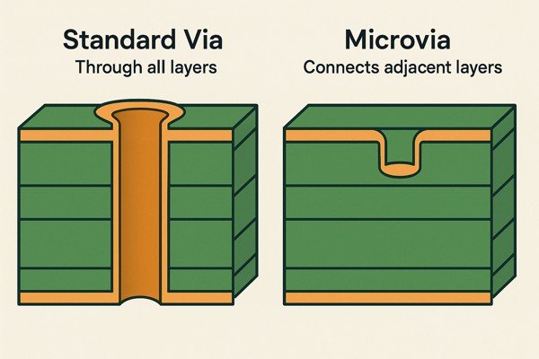
What is a microvia and when should it be used instead of a standard via?
You’re trying to route a 0.5 \(\text{mm}\) pitch BGA, but there’s no way to get a trace out from the inner balls. Standard vias are simply too large. This is the exact problem that microvias were invented to solve. 💡
A microvia is a laser-drilled via, typically 0.1 \(\text{mm}\) (4 \(\text{mils}\)) or smaller, that connects only adjacent layers (blind via) or an outer layer to the one just below it. You must use microvias for High-Density Interconnect (HDI) designs, especially for breaking out of fine-pitch BGAs (0.5 \(\text{mm}\) pitch or less).
Microvias: The Solution for High-Density Interconnect (HDI) PCBs
HDI technology is formally classified by the IPC-22264 standard based on the complexity of the board’s layer build-up. Understanding this helps you communicate your needs clearly to a fabricator.
| IPC-2226 Type | Structure Description | Complexity / Cost 💰 |
|---|---|---|
| Type I | 1 layer of microvias on a simple laminate core. | Low |
| Type II | 1 layer of microvias on a core that also contains buried mechanical vias. | Medium |
| Type III | 2+ layers of microvias on a core (enables stacked vias). | High |
| Any Layer HDI | A core-less build-up made entirely of HDI layers. | Very High |
For most BGA breakouts, a Type I or Type II structure is sufficient.
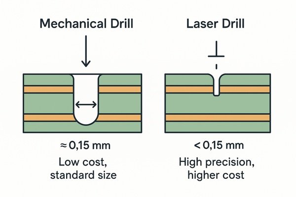
What are the limitations of mechanical drilling versus laser drilling for vias?
You know you need to create holes in your board, but should they be drilled with a bit or a laser? Choosing the wrong method can either limit your design’s density or massively inflate its cost. Understanding their core differences is key.
Mechanical drilling is the workhorse for cost-effective through-holes, with a practical lower limit of \(\approx\)0.15 \(\text{mm}\) (6 \(\text{mils}\)). Laser drilling is a premium process for creating much smaller vias (\(<\)0.15 \(\text{mm}\)) for HDI boards, but it’s more expensive.
Mechanical vs. Laser Drilling5: Choosing the Right Tool for Vias
The two technologies are optimized for completely different tasks.
| Feature | Mechanical Drilling ⚙️ | Laser Drilling ⚡ |
|---|---|---|
| Smallest Hole Size | \(\approx\)0.15 \(\text{mm}\) (6 \(\text{mils}\)) | \(\approx\)0.025 \(\text{mm}\) (1 \(\text{mil}\)), typically 0.1 \(\text{mm}\) |
| Via Type | Primarily Through-Holes | Primarily Blind Vias (one layer deep) |
| Aspect Ratio Limit | Plating-limited (\(<\)12:1) | Focus-limited (\(\approx\)1:1) |
| Special Process | Enables Back-drilling to remove stubs | Enables Via-in-Pad6 Plated Over (VIPPO) |
| Cost | Low | High |
| Primary Application | Standard PCBs, Power Boards | HDI, BGA Breakout, Miniaturization |
Often, a dual-laser process (CO₂ for bulk removal, UV for cleaning) is used to create the highest quality microvias.
How should the appropriate via size be selected for a PCB design?
You’re starting a new layout and it’s time to set up your design rules. Picking a via size can feel arbitrary, but making a thoughtful choice now will save you countless headaches during routing and manufacturing.
Always start with a standard, cost-effective via like a 0.3 \(\text{mm}\) drill / 0.6 \(\text{mm}\) pad as your default. Only deviate from this standard when a specific design constraint—such as BGA breakout, high-current needs, or routing density—absolutely forces you to use a smaller or larger size.
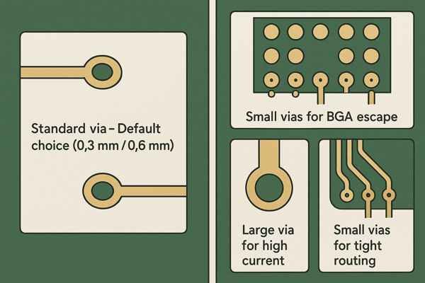
A Practical 5-Step Process for Selecting Via Sizes
This "Via Selection Cheat Sheet" summarizes the process I follow for every design.
| Design Consideration | Recommended Via Type | Key Parameter to Define | Rule of Thumb / Best Practice |
|---|---|---|---|
| General Routing | Standard Through-Hole | Drill/Pad Size | Start with 0.3\(\text{mm}\) / 0.6\(\text{mm}\). It’s cheap and reliable. |
| Fine-Pitch SMT/BGA | Smaller Through-Hole | Drill/Pad Size | Use 0.2\(\text{mm}\) / 0.45\(\text{mm}\) only where routing space is tight. |
| High Current (\(>\)1\(\text{A}\)) | Power Via(s) | Finished Hole Diameter | Use IPC-21527 calculator. Use multiple vias for \(>\)2\(\text{A}\). |
| Thermal Dissipation | Thermal Via Array | Via Quantity & Placement | Place an array of 0.3\(\text{mm}\) vias directly under the thermal pad. |
| High-Speed Signals | Impedance-Controlled Via | Antipod Diameter | Model with a field solver. Add ground return vias nearby. |
Following a structured approach like this ensures that every via on your board is fit for its specific purpose, balancing performance, density, and cost.
Conclusion
Choosing the right via is a core engineering decision. Always start with a robust, low-cost standard via and only shrink it when density forces your hand, always staying aware of your fabricator’s capabilities.
-
Learn how teardrops can reinforce PCB connections, prevent breakout, and improve manufacturing reliability in your circuit board designs. ↩
-
Explore this link to understand how Pulse Plating enhances copper deposition in PCBs, crucial for high aspect ratio applications. ↩
-
Learn why proper tooling is essential in PCB manufacturing to ensure accuracy, efficiency, and consistent quality. ↩
-
Exploring this link will provide you with a comprehensive understanding of the IPC-2226 standard, essential for effective communication with PCB fabricators. ↩
-
Discover laser drilling, a high-precision, non-contact technique using pulsed lasers to rapidly create tiny holes in various materials for industrial and medical applications. ↩
-
Discover how via-in-pad can benefit high-density PCB designs but demands precise manufacturing to avoid soldering issues. ↩
-
Learn how the IPC-2152 standard helps you accurately size vias for high-current PCB designs, ensuring reliability and safety in your circuits. ↩


