Your new PCB prototype has arrived. It looks perfect, but hidden thermal problems can cause instant failure. Knowing what to look for before and during that first power-on is critical.
During board bring-up, you can detect issues like short circuits, overloaded components, oscillating regulators, and poor thermal design. These problems show up as unexpected hot spots that a thermal camera or even a careful touch can find, preventing catastrophic damage to your prototype.
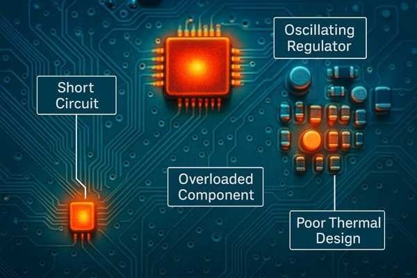
The first few seconds after powering on a new board are the most critical. This is when design flaws, assembly errors, or faulty components often reveal themselves through excess heat. A systematic approach to bring-up helps you catch these issues early, saving countless hours of difficult debugging later. Let's break down how to find and understand these thermal problems.
What Are The Essential Tools For Board Bring-up and Thermal Analysis?
You have a new board, but do you have the right tools? Without them, you're essentially flying blind, risking damage with every test. The right gear makes finding heat problems simple.
For effective thermal analysis during bring-up, you need a DC power supply with an adjustable current limit, a digital multimeter (DMM), an oscilloscope, and a thermal camera. These tools allow you to control power, measure key values, and see heat signatures directly.
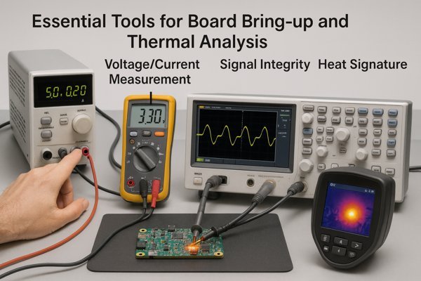
Each tool has a specific job in finding thermal issues. In my experience, having these ready before I even think about plugging in a board has saved me from destroying expensive prototypes. At Honeywell, on the Tuxedo Keypad project, our bring-up checklist always started with verifying our test bench was fully equipped. A missing tool, especially the current-limited supply, was a non-starter. You don't just need the tools; you need to know how to use them to hunt for heat.
The Four Essential Tools for Thermal Triage
These four tools work together to create a safety net, allowing you to control, observe, and measure the board's behavior. The power supply acts as a gatekeeper, the DMM as a pre-flight checker, the thermal camera as your heat-vision, and the oscilloscope as a detector for invisible problems like instability, which often manifests as heat. When a regulator gets hot for no obvious reason, the scope is often the tool that reveals the high-frequency oscillation silently burning up power.
Essential Tool Breakdown and Pro-Tips
| Tool | Primary Function for Thermal Analysis | My Pro-Tip |
|---|---|---|
| DC Power Supply | Safely apply power with a strict current limit. An abnormal current draw is the first sign of a problem that generates heat. | Start with a very low current limit, maybe 50-100 mA, for the very first power-on. If the supply hits the limit, you have a short. Don't increase it. |
| Digital Multimeter (DMM) | Measure resistance on unpowered rails to find shorts before applying power. Also used to verify voltages are correct once powered. | Use the "diode check" or continuity mode to check power rails against ground. A reading near zero ohms means you have a direct short. |
| Thermal Camera | Instantly visualize heat across the entire board. It's the fastest way to find an overheating component without touching anything. | Even an entry-level thermal camera for your smartphone is a game-changer. It can spot a 10°C rise in seconds, pointing you directly to the problem area. |
| Oscilloscope | Check for high-frequency oscillations on regulators or op-amps. These oscillations don't always draw huge DC current but cause components to get very hot. | Use a 10x probe with a short ground lead. Look for fuzzy, thick waveforms on regulator outputs where you expect a clean DC line. Zoom in on the timebase to see the high-frequency ringing. |
What Is The Safe Procedure For The First Power-on of a New Pcb?
The moment of truth arrives: the first power-on. A wrong move here can turn your brand-new board into a paperweight. A disciplined, step-by-step process is your best defense against failure.
A safe power-on involves a pre-power visual inspection, checking for shorts with a DMM, and using a current-limited power supply set to a minimal value. You then apply power briefly, check for hot spots, and only gradually increase voltage and current limits.
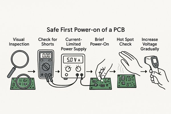
This procedure might seem slow, but it's far faster than debugging a board you've just damaged. I learned this the hard way early in my career when I powered a board with a reversed tantalum capacitor. The pop was loud, and the damage was permanent. Now, I follow a strict checklist for every new board. This structured approach methodically reduces risk by checking for different types of faults at each stage.
Step-by-Step Power-On Checklist
| Step | Action | Purpose | What to Look For |
|---|---|---|---|
| 1 | Visual Inspection | Catch physical assembly errors. | Solder bridges, incorrect component orientation, tombstoned parts, missing components. |
| 2 | Resistance Checks | Find shorts on power rails before applying voltage. | Use a DMM to check resistance from each power rail to GND. A value < 10 Ω is a likely short. |
| 3 | Set Power Supply | Prepare for a safe, low-power test. | Set voltage to the board's primary rail. Set current limit to a minimal value (e.g., 50 mA). |
| 4 | "Flicker Test" | Apply power for only 1-2 seconds. | Watch the power supply's current meter. If it instantly hits the limit, you have a hard short. |
| 5 | "Touch Test" / Thermal Scan | Detect immediate overheating. | With power off, carefully touch major ICs or scan with a thermal camera. Nothing should be warm. |
| 6 | Gradual Power-Up | Bring the board up while monitoring it. | If the flicker test passes, power on and watch the current draw. It should be stable and low. |
What to Do When a Check Fails
Following a procedure is great, but knowing what to do when something goes wrong is even more important. A failed check is not a dead end; it's the start of the real debugging process. If a visual inspection fails, you must stop and send the board for rework. If the resistance check fails, do not apply power. The most common culprit is a failed ceramic bypass capacitor, so begin checking the caps on the shorted rail. If the flicker test fails, the power supply hitting its current limit confirms a hard short; the heat generated, even for a second, can often be seen by a thermal camera, pointing you directly to the faulty component.
| Failure Point | Immediate Action | Next Diagnostic Step |
|---|---|---|
| Visual Inspection | STOP. Do not proceed to power-on. | Document the specific error with photos. Contact the assembly house for rework or guidance. |
| Resistance Check | STOP. Do not apply power. | Begin isolating the shorted rail. Start by checking the resistance of all ceramic capacitors on that rail, as they are a common failure point. |
| "Flicker Test" | STOP. Power off immediately. | The short is confirmed. Use a thermal camera to see if the brief power pulse created a hot spot, which can pinpoint the faulty component. |
What Are The Common Signs of a Short Circuit on a PCB During Bring-up?
You power on the board and something is wrong. A short circuit is a common culprit, but its signs can vary. Knowing the symptoms helps you diagnose the problem quickly and safely.
The most common signs of a short circuit are the power supply immediately hitting its current limit, a specific component getting extremely hot, or a voltage rail measuring 0V. Sometimes, you might even smell burning or see a wisp of smoke.
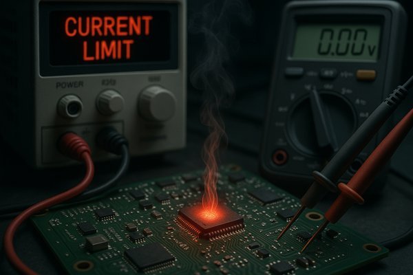
A short circuit provides a low-resistance path for current to flow, usually from a power rail directly to ground. This massive current flow, governed by Ohm's Law (\(I = V/R\)), is what generates the intense heat that can damage your board. When I was bringing up the PACE evaluation board at Lightelligence, we had a tiny solder bridge under a BGA chip. The board drew almost 5 amps at 1.2V on first power-on. The thermal camera immediately showed the BGA glowing red hot, and we knew exactly where the short was.
Troubleshooting Guide for Short Circuit Symptoms
| Symptom | What It Means | First Investigation Step |
|---|---|---|
| Current Limit Hit Instantly | A very low-resistance path ("dead short") exists on the main power input. | Disconnect power. Use your DMM's continuity mode to find the rail that is shorted to ground. |
| A Single Hot Component | Heat is concentrated. This could be an internally failed component or a backward-installed part. | Use a thermal camera to pinpoint the hot IC. Power down and check the resistance of its output pins to ground. |
| Voltage Rail at 0V | The short is pulling so much current that it's causing the supplying voltage regulator to shut down. | This confirms the short is on a specific rail. Focus your DMM resistance checks on the components connected to that rail. |
| Audible Buzz or Smell | A component is under extreme stress and on the verge of catastrophic failure. | Immediately disconnect all power. Visually inspect for scorch marks or physical damage. |
Advanced Short-Finding Techniques
When your DMM isn't enough to find a tricky short (like one with ~1-2 ohms of resistance), you need more advanced methods. One is low-voltage injection, where you use a lab supply to inject a low voltage (e.g., 0.5 V) and high current (1-2 A) into the shorted rail. The component that is truly shorted will heat up significantly, making it easy to spot with a thermal camera. Another is a four-wire (Kelvin) measurement1 using a high-quality bench DMM. This method eliminates the resistance of the test leads, allowing you to precisely measure milliohm differences along a power plane to trace the path of lowest resistance to the short.
| Technique | Best For | How It Works | Cautions |
|---|---|---|---|
| Low-Voltage Injection | Finding low-resistance shorts (\(<1 \text{ Ω}\)) on complex boards. | Inject a low voltage (e.g., 0.5V) and high current (1-2A) into the shorted rail. The shorted component heats up significantly due to \(I^{2}R\) power loss. | Use a dedicated short-finding tool or be very careful with a lab supply. Do not exceed the voltage rating of the components on the rail. |
| Four-Wire (Kelvin) Measurement | Precisely measuring resistance to trace the path of a short. | A bench DMM uses four wires (two for current, two for voltage sensing) to eliminate test lead resistance, allowing for accurate milliohm measurements. | Requires a specialized DMM. Best for tracing shorts across large ground planes or wide power traces where voltage drops are tiny. |
How Can a Thermal Camera Be Used to Debug a New Circuit Board?
You have a problem, but your eyes can't see it. A thermal camera can reveal hidden issues instantly. It's like giving yourself superpowers for electronics debugging, showing you exactly where to look.
A thermal camera detects infrared radiation and translates it into a visual image, showing the temperature distribution across your board. This allows you to instantly spot short circuits, stressed components, or inefficient power conversion as bright, hot spots, guiding you directly to the root of the problem.
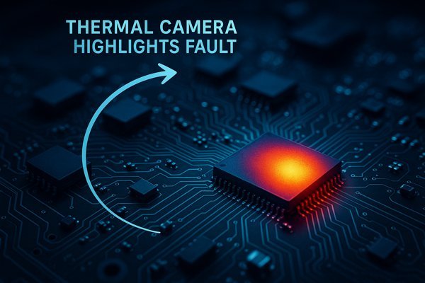
Using a thermal camera is straightforward, but interpreting the results is a skill. It's not just about finding the hottest spot; it's about understanding what "normal" looks like for your board and identifying deviations from that baseline. Before I even power on a board, I have a mental map of where I expect to see heat: the voltage regulators, the processor core, and any high-current drivers. Anything outside of those areas getting warm is an immediate red flag.
Why Emissivity Affects Thermal Camera Accuracy
A critical concept for accurate thermal measurement is emissivity2. This is a measure of how effectively a surface radiates thermal energy, on a scale from 0 to 1. Shiny surfaces, like a solder joint, have low emissivity and will reflect the infrared radiation from their surroundings, making them appear cooler than they actually are. Matte surfaces, like the black plastic of an IC package, have high emissivity (close to 1) and give a much more accurate reading. To get reliable measurements across a board, apply a small patch of material with a known, high emissivity (like a piece of electrical tape or special matte spray) to the components you want to measure accurately.
| Surface Material | Typical Emissivity (ε) | Appearance in Thermal Image (if uncorrected) |
|---|---|---|
| Black IC Package (Matte) | ~0.95 | Accurate Temperature |
| Green Solder Mask | ~0.92 | Mostly Accurate |
| Solder (Shiny) | 0.1 - 0.3 | Appears much cooler than its actual temperature |
| Bare Copper (Shiny) | ~0.05 | Appears very cool, highly reflective |
Common Thermal Signatures and Their Meanings
| Thermal Signature | Possible Cause(s) | Next Step |
|---|---|---|
| One intensely hot, small spot | A short circuit, often caused by a solder bridge or a failed ceramic capacitor. | Power off. Use a DMM to confirm a low-resistance short at that location. |
| A warm, but not hot, component | A component drawing more quiescent current than expected, a minor logic contention, or an oscillating amplifier. | Check the component's current draw. Probe its outputs with an oscilloscope. |
| A warm trace or wire | Higher than expected current is flowing through that conductor. | Calculate the expected current for that trace. Check the load it is powering for faults. |
| Entire board is slightly warm | Inefficient power regulation or a higher-than-expected idle current for the entire system. | Measure the total current draw and compare it against your power budget. |
What Causes a Voltage Regulator or LDO to Overheat Immediately at Power-on?
You power up the board and the voltage regulator is instantly hot enough to burn your finger. This common problem can be frustrating. It almost always points to a few specific, fixable issues.
A voltage regulator or LDO typically overheats immediately due to a short circuit on its output, an excessive load, high-frequency oscillation, or reversed input polarity. Each of these conditions forces the regulator to dissipate far more power than it was designed for, converting electricity directly into heat.
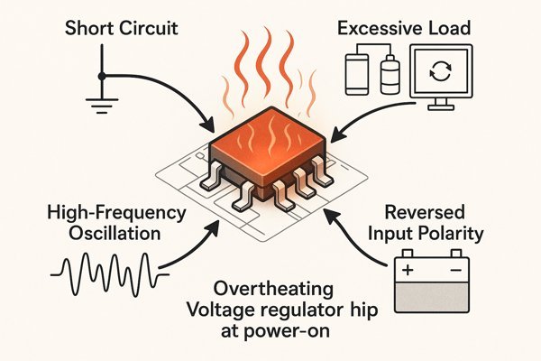
When I was at Smiths Medical developing an infusion pump, we had an LDO that kept overheating. The output had no short, and the load was minimal. The problem turned out to be oscillation. The output capacitor we chose had too low of an ESR (Equivalent Series Resistance), which made the LDO's control loop unstable. The LDO was oscillating at several MHz, and this high-frequency switching was burning up power inside the chip. An oscilloscope on the output revealed the problem instantly.
Troubleshooting Checklist for an Overheating Regulator
| Potential Cause | How to Verify | Solution |
|---|---|---|
| Shorted Output | Power down. Use a DMM to measure resistance from the regulator's output pin to ground. A reading near \(0 \text{ Ω}\) confirms a short. | Find and fix the short on the output rail. Check for failed bypass capacitors or solder bridges. |
| Excessive Load | The current draw is higher than the regulator's rating, but it's not a direct short. | Isolate the load from the regulator and power the load separately to measure its current draw. Fix the downstream circuit. |
| Instability / Oscillation | Use an oscilloscope with a 10x probe on the regulator's output. Look for high-frequency noise or ringing. | Check the regulator's datasheet for required output capacitor type, value, and \(ESR\). You may need to change the capacitor. |
| Incorrect Installation | The regulator is installed backward, or the input and output pins are swapped. | Visually inspect the component's orientation against the PCB silkscreen and layout. Correct the installation. |
| Input Voltage Too High | The voltage drop across the LDO (\(V_{IN} - V_{OUT}\)) is excessive, causing high power dissipation (\(P_{D} = (V_{IN} - V_{OUT}) \times I_{LOAD}\)). | Verify the input voltage. If it is correct but dissipation is too high, you may need a switching regulator instead of an LDO. |
What Causes an FPGA or CPU to Get Hot Without Any Firmware Loaded?
Your main processor or FPGA is getting hot, but you haven't even loaded firmware. This is a scary problem. It often points to a fundamental hardware issue with the board or the chip itself.
An FPGA or CPU can get hot without firmware due to shorted power or I/O pins, contention between I/O banks powered by different voltages, a manufacturing defect in the chip, or a latch-up condition caused by improper power sequencing. These issues cause uncontrolled current flow.
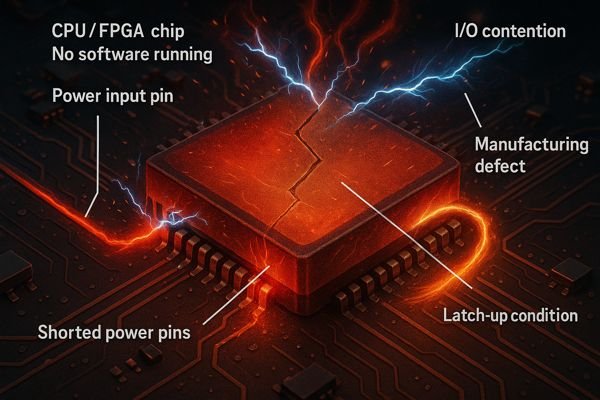
On a large board with a multi-rail BGA chip, this is a particularly tough problem to debug. The first thing I do is re-verify the power rails. Use a DMM to check every single power pin on the device for shorts to ground or shorts to adjacent rails. Next, think about I/O pins. Are any pins that default to outputs at power-on connected together? Or is an output pin tied directly to ground or VCC? This creates a direct path for current to flow.
Using JTAG Boundary Scans for Pre-Power-On Checks
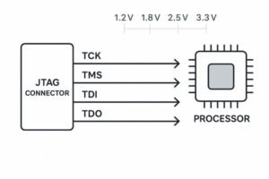
For complex devices like FPGAs, a powerful tool to use before the first power-on is a JTAG boundary scan. This test can check for open circuits (like a non-soldered BGA ball) and short circuits between I/O pins without powering up the core logic. Running a boundary scan can catch many common manufacturing defects that would otherwise cause the chip to get hot on first power-on, saving you from potentially damaging an expensive component.
Common Causes for Pre-Firmware Overheating
| Cause | Description | How to Debug |
|---|---|---|
| Shorted Power Pins | A solder bridge or internal defect is shorting a power rail (e.g., 1.2V core) to ground or another rail. | Power off. Use a DMM to meticulously check the resistance of every power and ground pin on the BGA to its neighbors. |
| I/O Pin Contention | Two I/O pins that default to an output state are tied together in the schematic, fighting each other. | Review the schematic and the chip's default pin states in the datasheet. Look for any direct conflicts. |
| Improper Power Sequencing | An I/O voltage (e.g., 3.3V) comes up before the core voltage (e.g., 1.2V), causing latch-up. | Check the datasheet's power sequencing requirements. Use an oscilloscope to probe the power rails during startup and verify they turn on in the correct order. |
| Manufacturing Defect | The silicon die itself has a flaw, causing an internal short. This is less common. | This is a diagnosis of last resort. If all other possibilities are exhausted, try replacing the chip. |
How Can Current Draw Be Measured Accurately to Detect Thermal Problems?
You suspect a thermal problem, and you know it's related to power consumption. But how do you measure it accurately? Getting a precise current measurement is key to confirming your suspicions and finding the fault.
Accurate current draw can be measured using the built-in meter on a bench power supply for a general idea, a DMM in series with the power rail for high precision at low currents, or a dedicated current probe with an oscilloscope for dynamic loads.
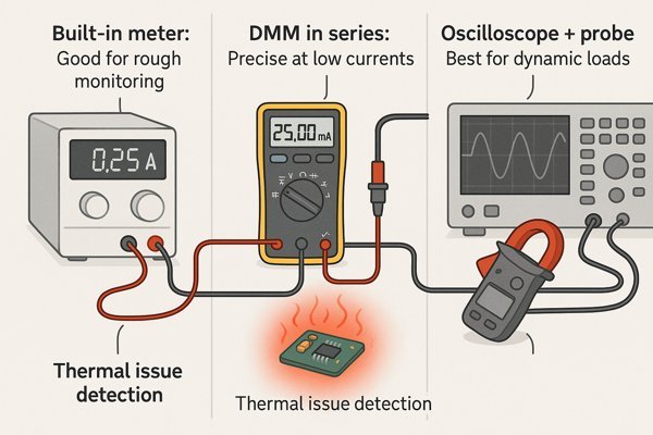
Each method has its trade-offs. The right choice depends on whether you need a quick check, a precise average, or a view of dynamic behavior. For example, the bench supply might show an average of 150 mA, but a current probe could reveal that the circuit is actually drawing 1A for short bursts, which could be the source of your thermal issue.
How to Design-In Shunt Resistors for Current Measurement
For a permanent and accurate measurement point, I often design a small shunt resistor3 directly into the power path of a critical rail. A shunt is a very low-value, high-precision resistor (e.g., \(10 \text{ m}\Omega\)). By placing probe points across this resistor, you can use a sensitive DMM or an oscilloscope to measure the small voltage drop. Using Ohm's Law (\(I = V/R\)), you can calculate the current. When choosing a value, it's a trade-off: a larger resistance gives you a larger, easier-to-measure voltage drop, but it also wastes more power (\(P = I^{2}R\)) and reduces the voltage supplied to the load (known as "\(IR\) drop").
| Target Current Range | Example Shunt Value | Voltage Drop at Max Current | Power Dissipation at Max Current |
|---|---|---|---|
| 0 - 100 mA | 1 Ω | 100 mV | 10 mW |
| 0 - 1 A | 0.1 Ω (100 mΩ) | 100 mV | 100 mW |
| 0 - 5 A | 0.01 Ω (10 mΩ) | 50 mV | 250 mW |
| 0 - 10 A | 0.005 Ω (5 mΩ) | 50 mV | 500 mW |
Comparison of Current Measurement Techniques
| Method | Best For | Pros | Cons |
|---|---|---|---|
| Bench Power Supply Meter | Quick, rough check of total board consumption. | Very convenient, no circuit modification needed. | Low accuracy, slow update rate, cannot see dynamic changes. |
| DMM (Ammeter Mode) | Measuring stable, DC current for a specific rail. | High accuracy and resolution for DC measurements. | Must break the circuit to insert the meter. The meter's "burden voltage" can affect the circuit. |
| Oscilloscope + Current Probe | Visualizing dynamic, time-varying current. | See real-time current waveforms, inrush currents. | Probes are expensive. Lower accuracy than a good DMM for DC. |
| Shunt Resistor + Voltmeter | Built-in, permanent current measurement point. | Low cost, allows for continuous monitoring. | Requires careful design, introduces a small voltage drop. |
What Is a Normal Operating Temperature for Components Like Processors and Power Ics?
Your component feels hot to the touch, but is it too hot? Without knowing the component's limits, you can't tell if you have a real problem. "Hot" is subjective; datasheets provide the facts.
A normal operating temperature depends on the component and its rating. Most commercial-grade ICs are rated for a case temperature up to \(70^\circ\text{C}\) or \(85^\circ\text{C}\). The critical value is the maximum junction temperature (\(T_{J}\)), often \(125^\circ\text{C}\) or \(150^\circ\text{C}\), which is the internal temperature of the silicon.
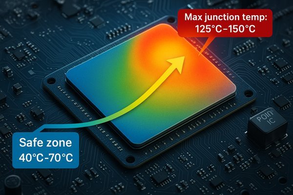
The first place to look is always the component's datasheet under "Absolute Maximum Ratings" and "Thermal Information." You'll find the maximum junction temperature (\(T_{J}\)) and the thermal resistance values. As a rule of thumb, if a component is too hot to comfortably keep your finger on it for more than a few seconds (around \(50-60^\circ\text{C}\)), it's worth checking the datasheet.
The Importance of Derating for Reliability
Just because a component can run at a \(T_{J}\) of \(125^\circ\text{C}\) doesn't mean it should. Operating continuously at maximum temperature significantly reduces the lifespan and reliability of a component. The failure rate of semiconductors increases exponentially with temperature. For high-reliability applications like medical or aerospace systems, we practice "derating." This means we design the system so that components operate at a junction temperature significantly below their maximum rating. A common target is to keep \(T_{J}\) below \(105^\circ\text{C}\), even if the part is rated for \(125^\circ\text{C}\). This \(20^\circ\text{C}\) margin provides a buffer and ensures a much longer product life.
| Parameter | Absolute Max (Datasheet) | High-Reliability Derated Target | Rationale |
|---|---|---|---|
| Junction Temperature (\(T_{J}\)) | \(125^\circ\text{C}\) | \(< 105^\circ\text{C}\) | A \(20^\circ\text{C}\) margin dramatically improves lifespan and reliability (\(MTBF\)). |
| Voltage Rating | 20 V | \(< 16 \text{ V}\) (80% of max) | Provides a buffer against transient voltage spikes and reduces electrical stress. |
| Power Dissipation | 1 W | \(< 0.7 \text{ W}\) (70% of max) | Ensures the component runs cooler and has headroom for thermal variations. |
Typical Operating Temperature Grades
| Grade | Ambient Operating Range (\(T_{A}\)) | Typical Max Junction Temp (\(T_{J}\)) | Application Examples |
|---|---|---|---|
| Commercial | \(0^\circ\text{C}\) to \(70^\circ\text{C}\) | \(125^\circ\text{C}\) | Consumer electronics, office equipment |
| Industrial | \(-40^\circ\text{C}\) to \(85^\circ\text{C}\) | \(125^\circ\text{C}\) | Factory automation, control systems |
| Automotive (AEC-Q100) | \(-40^\circ\text{C}\) to \(125^\circ\text{C}\) (Grade 1) | \(150^\circ\text{C}\) | In-vehicle electronics, engine control units |
| Military | \(-55^\circ\text{C}\) to \(125^\circ\text{C}\) | \(150^\circ\text{C+}\) | Aerospace, defense systems |
Can an Incorrect Component Orientation or a Tombstoned Part Cause Overheating?
You've checked the design, but the problem is on the board itself. A simple assembly mistake can easily lead to a serious thermal issue. These are often the first things to look for.
Yes, absolutely. An incorrect component orientation, such as a reversed diode or polarized capacitor, can create a short circuit and cause immediate overheating. A tombstoned component can open a critical circuit path, like a feedback loop, causing a regulator to fail and overheat.
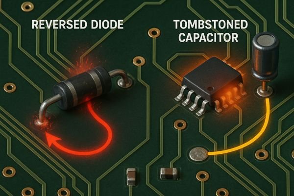
These are manufacturing defects, but they show up as electrical and thermal problems during bring-up. A reversed tantalum capacitor will act like a short and often fail spectacularly. A reversed diode will either block current when it should conduct or conduct when it should block, both of which can lead to overheating in other parts of the circuit. This is why a thorough visual inspection under magnification is the very first step of any board bring-up.
Common Assembly Errors and Their Thermal Consequences
| Assembly Error | Electrical Consequence | Thermal Result |
|---|---|---|
| Reversed Polarized Capacitor | The capacitor acts as a low-resistance short circuit when reverse-biased. | Intense, localized heating of the capacitor itself, often leading to it venting or exploding. |
| Reversed Diode / LED | The diode conducts when it should block (or vice versa), shorting a power rail or failing to protect a circuit. | Heating of the diode and/or other components in the path due to unexpected high current. |
| Incorrect IC Orientation | Power and ground pins are connected to the wrong signals, and I/O pins are mismatched. | Severe internal shorting within the IC, causing it to heat up rapidly and likely suffer permanent damage. |
| Tombstoned Resistor | The resistor lifts off one pad, creating an open circuit. | If in a regulator's feedback path, the output voltage can spike, causing the regulator and downstream components to overheat. |
How Can a Faulty Component Be Differentiated From a Design Flaw When Diagnosing a Hot Spot?
You've found a hot spot. Now for the hard question: is the component bad, or is your design asking it to do something impossible? Differentiating between these two is a critical debugging skill.
To differentiate a faulty component from a design flaw, first, analyze the circuit to see if the component is being operated within its datasheet limits. If the design seems correct, replace the suspect component with a new one. If the problem disappears, the original component was likely faulty.

This process is one of elimination. I always start by assuming the design is flawed, as that's more common than a brand new component being dead on arrival. I once spent two days debugging a power supply where an LDO was overheating. The design looked perfect, my calculations were right, and the load was correct. I was convinced my layout was causing an oscillation I couldn't capture. As a last resort, I swapped the LDO with one from a different reel. The problem vanished. It turned out the entire batch of regulators we received had a manufacturing defect. It's a good lesson: always validate your design, but don't rule out a bad part.
Troubleshooting Process: Design Flaw or Faulty Part?
| Step | Question to Answer | Action | Implication if Problem is Solved |
|---|---|---|---|
| 1. Sanity Check | Is the component operating within its datasheet limits according to the design? | Review schematic, check calculations for power, voltage, current. Compare against datasheet absolute maximum ratings. | N/A (This step identifies design flaws). |
| 2. Isolate | Is an external factor causing the issue? | Disconnect the load from the hot component. Power other sections of the board independently if possible. | The problem is in the load or another interacting circuit, not the component itself. |
| 3. Replace | Is the specific component defective? | Carefully desolder the hot component and replace it with a brand new one (ideally from a different batch). | The original component was faulty (e.g., damaged by ESD, manufacturing defect). |
| 4. Replicate | Does the issue only occur under specific conditions? | Vary the input voltage, load, or ambient temperature within the intended operating range. | The design has a marginality issue; it's not robust. It's a design flaw that needs correction. |
What Role Do Ground Planes and Power Planes Play in Thermal Dissipation?
You might think of ground and power planes as just electrical pathways. But they are also your board's most powerful, built-in cooling system. Ignoring their thermal role is a common design mistake.
Ground and power planes act as large, flat heat sinks integrated directly into the PCB. They dissipate heat by spreading it laterally away from hot components and vertically to other layers. A large, unbroken copper plane offers a low thermal resistance path to the surrounding air.
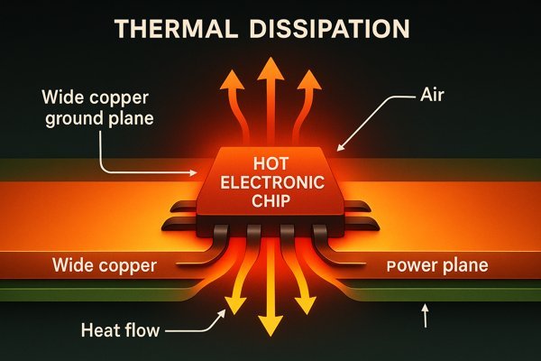
Heat wants to move from a hot area to a cooler one, and thick copper planes are excellent conductors of heat. When a component's thermal pad is connected to a large ground plane, the heat doesn't stay concentrated under the part. Instead, it spreads out across the area of the plane.
Example Heat Dissipation vs. Copper Area
The effectiveness of a copper plane is significant. Application notes from component manufacturers provide useful estimates for PCBs in open air with natural convection.
| Copper Area (1 oz, top layer) | Approx. Power Dissipation Capability | Equivalent To |
|---|---|---|
| Minimal Pad Size | ~0.5 W | A very poor heatsink. |
| 1.0 sq inch (~6.5 cm²) | ~1.2 W | A small, dedicated heatsink. |
| 2.5 sq inch (~16 cm²) | ~1.8 W | A medium heatsink. |
| 5.0 sq inch (~32 cm²) | ~2.2 W | A moderately large heatsink. |
Note: These are typical estimates. Actual performance depends heavily on airflow, board thickness, and internal planes.
Plane Design Best Practices
| Parameter | Good Practice | Bad Practice (Reduces Thermal Performance) |
|---|---|---|
| Continuity | Keep planes as solid and unbroken as possible. | Slicing planes into small, isolated islands with too many traces or cutouts. |
| Area | Maximize the copper area connected to the heat source. | Using only thin thermal reliefs to connect a component pad to the plane. |
| Connections | Connect component thermal pads directly to the plane, often with multiple vias. | No direct connection, or relying on only signal traces to carry heat. |
| Layer Stacking | Place hot components on outer layers with planes directly underneath them. | Burying a high-power plane deep inside the board stack-up with no thermal vias. |
How Do Thermal Vias Function to Dissipate Heat?
You've connected your component to a ground plane on the top layer, but it's still too hot. How do you get that heat to the other layers? The answer is thermal vias.
Thermal vias are small plated holes that create a thermal path to transfer heat from a component on the top layer of a PCB down to internal or bottom copper planes. They act like metal pillars, providing a low thermal resistance path through the non-conductive PCB substrate.
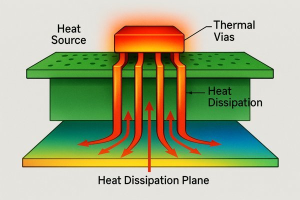
The core material of a PCB, like FR-4, is a very poor conductor of heat (a thermal insulator). Placing a hot component on the board is like putting a hot pan on a wooden table—the heat stays concentrated. Thermal vias solve this by creating multiple parallel paths for heat to travel through the insulating FR-4 to other copper layers, which can then spread the heat out.
Key Design Parameters for Effective Thermal Vias
| Parameter | Recommendation | Rationale |
|---|---|---|
| Quantity | Use as many vias as can reasonably fit under the thermal pad. | Thermal resistance is reduced in parallel. More vias = lower total resistance. |
| Diameter | 0.3mm to 0.5mm (12 to 20 mils) is a common range. | A good balance between thermal performance and manufacturability. Prevents excessive solder wicking if left open. |
| Plating Thickness | 1 oz (35µm) copper or more if possible. | Thicker copper plating provides a better thermal path through the via barrel. |
| Filling (Optional) | For best performance, fill vias with thermally conductive epoxy and cap (plate over) them. | Eliminates air voids and provides a solid thermal path. Prevents solder paste from wicking away from the component pad during reflow. This adds cost. |
| Placement | Place vias directly on the component's thermal pad in a grid pattern. | This provides the most direct path for heat to escape from the source. |
What Is The Method For Verifying The Effectiveness of Thermal Vias?
You added thermal vias to your design, trusting they would help with cooling. But how do you know they're actually working? You need to test and verify their performance on the real board.
The effectiveness of thermal vias is best verified using a thermal camera to compare the temperature of the component with and without a proper thermal connection. You can also use thermocouples for precise point measurements and compare the results against your initial thermal simulation data.
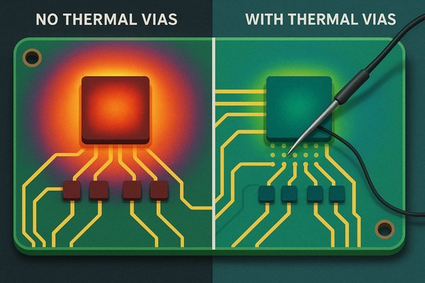
The most direct method is an A/B test4. If you have a prototype where the thermal vias were not tented and were filled with solder paste, and another where they were not, you can measure the temperature difference under the same load. A well-designed thermal via array can lower a component's case temperature by 10-30°C compared to a design with no vias. When I'm validating a new high-power design, I get very quantitative about it.
Comparison of Verification Methods
| Method | Description | Pros | Cons |
|---|---|---|---|
| Thermal Camera Imaging | Use an IR camera to visually compare the temperature of the component case and the temperature on the opposite side of the PCB. | Quick, non-contact, gives a great visual representation of heat spreading. | Measures surface temperature, not internal junction temperature. Emissivity of surfaces can affect accuracy. |
| Thermocouple Measurement | Attach fine-gauge thermocouples directly to the component case and to the copper plane on the bottom side of the board. | High accuracy for point measurements. Allows for direct calculation of thermal resistance (\(\Delta T / P_{D}\)). | Invasive (requires gluing probes), measures only a single point, can be difficult to attach properly. |
| Comparison to Simulation | Run the board under a known, fixed load and measure the resulting component temperature. Compare this value to the temperature predicted by your thermal simulation. | Directly validates the accuracy of your design models. Helps you improve future simulations. | Requires an accurate power dissipation value for the component, which can sometimes be hard to determine. |
What Are The Best Design Practices for PCB Thermal Management?
Fixing thermal problems during bring-up is stressful and expensive. The best approach is to design for good thermal performance from the very beginning. A few key practices can prevent most common heat issues.
The best practices for PCB thermal management include placing hot components away from sensitive ones, using large copper planes for heat spreading, implementing thermal vias under power components, using wider traces for high currents, and considering the board's orientation and airflow early in the design process.
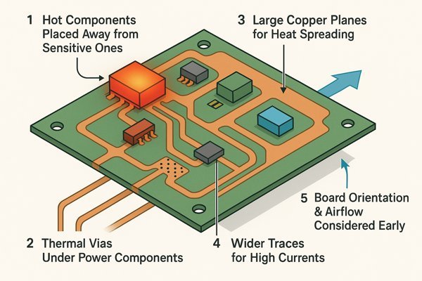
Good thermal design is about giving heat an easy path to escape. I treat it as a fundamental part of the layout process, not an afterthought. For the Tuxedo Keypad, we had a powerful processor in a sealed plastic case with no fan. We relied entirely on the PCB to act as the heatsink. This meant every detail, from component placement to copper pours, was optimized for heat dissipation.
Balancing Performance and Manufacturability with Thermal Reliefs
For non-power pins on a high-power component (like signal pins on a large QFN package), you should still use thermal reliefs when connecting them to a large plane. A direct connection can make soldering difficult, as the plane wicks heat away from the soldering iron too quickly, potentially leading to a cold solder joint. However, for the main thermal pad and high-current power pins, a direct, solid connection (a "flood") is almost always preferred to maximize thermal and electrical conductivity. It's a trade-off between manufacturability and performance.
| Connection Type | Best For | Pros | Cons |
|---|---|---|---|
| Direct Connect (Flood) | Thermal pads, high-current power pins, ground connections. | Lowest thermal and electrical resistance. Maximizes heat transfer. | Can make manual soldering difficult as the plane wicks away heat. |
| Thermal Relief (Spokes) | Non-power pins, signal pins on large components, through-hole component pins. | Prevents cold solder joints by limiting heat flow into the plane during soldering. | Higher thermal and electrical resistance. Should not be used for primary heat transfer paths. |
Thermal Design Checklist
| Design Stage | Best Practice | Rationale |
|---|---|---|
| Floorplanning | Place high-power components near the center of the board and away from edges. Separate hot components from thermally sensitive ones. | Allows heat to spread in all directions. Prevents heat from one component from degrading the performance or lifespan of another. |
| Layer Stackup | Use solid ground or power planes directly adjacent to layers with hot components. Use thicker copper (e.g., 2 oz). | Provides a low-resistance path for heat to spread. Thicker copper has lower thermal resistance. |
| Component Layout | Connect thermal pads to large copper pours and stitch with an array of thermal vias to other planes. | Creates a 3D heat-spreading structure, pulling heat away from the component both laterally and vertically. |
| Trace Routing | Use a trace width calculator based on the IPC-21525 standard for high-current traces. Be generous with width. | Prevents the traces themselves from becoming significant heat sources (\(P = I^{2}R\)). |
| System Level | Consider the enclosure and airflow early. If the board is in a sealed box, the PCB must dissipate all the heat. | The system environment defines the ultimate boundary condition for how heat can escape from the PCB. |
How Is a Thermal Simulation Performed Prior to PCB Manufacturing?
Can you find thermal problems before you even create your first prototype? Yes. Thermal simulation allows you to test your design in a virtual environment, saving time and money on costly respins.
A thermal simulation is performed by importing the PCB layout from an ECAD tool into a simulation software. The engineer then assigns power dissipation values to components, defines material properties and boundary conditions like ambient temperature and airflow, and the software solves for the resulting temperature distribution.
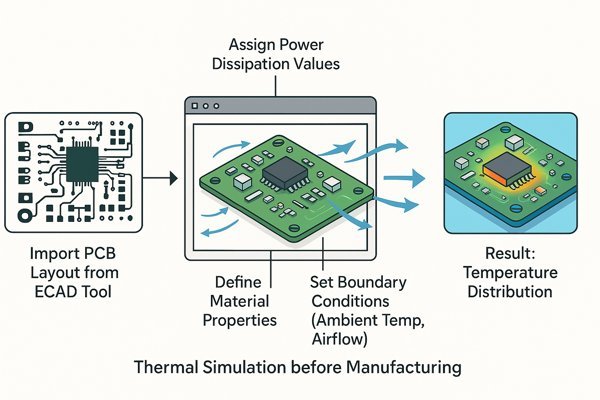
The process starts with your completed PCB layout. You export the board geometry and import it into a tool like Ansys Icepak, SolidWorks Flow Simulation, or HyperLynx Thermal. The next step is critical: defining the inputs. You have to tell the software how much heat each component generates. This data comes from datasheets or your own power consumption estimates.
Understanding Simulation Limitations and Real-World Correlation
A simulation is only a model of reality, and it's only as good as the data you feed it. The biggest source of error is often an inaccurate power dissipation value for the components. Therefore, simulation is best used to compare the relative performance of different design choices. After you build the first prototype, it is crucial to perform real-world temperature measurements and correlate them with your simulation results. This feedback loop allows you to refine your models, making your future simulations much more accurate and trustworthy.
| Aspect | Simulation | Real-World Measurement |
|---|---|---|
| Purpose | To predict thermal performance and compare design alternatives before manufacturing. | To validate the design and the simulation model after manufacturing. |
| Key Strength | Allows for rapid, low-cost iteration of design ideas (e.g., adding vias, increasing copper). | Provides the "ground truth" of how the board actually performs. |
| Main Weakness | Accuracy is highly dependent on the quality of the input data (especially power dissipation). | Can be time-consuming, requires physical hardware, difficult to isolate single variables. |
| Best Used For | Identifying major design flaws and optimizing the relative performance of thermal solutions. | Final design validation, quality control, and refining future simulation models. |
Key Inputs for an Accurate Simulation
| Input Parameter | Description | Source of Data |
|---|---|---|
| Geometry | The physical layout of the board, including all copper layers, vias, and components. | Exported directly from your ECAD tool (e.g., Altium Designer, Cadence Allegro). |
| Component Power Dissipation | The amount of heat (in Watts) generated by each active component. This is the most critical input. | Component datasheets, power budget calculations, or measurements from a previous design. |
| Material Properties | The thermal conductivity of the PCB substrate (e.g., FR-4), copper, component packages, etc. | Material datasheets, software libraries. |
| Boundary Conditions | The environment surrounding the PCB. This includes ambient temperature, airflow, and gravity orientation. | System requirements, intended use case of the product. |
Conclusion
Detecting thermal issues during bring-up is not luck; it is a skill. A methodical process and the right tools can reveal hidden problems before they cause irreversible damage to your hardware.
-
Learn about four-wire measurement techniques to improve your accuracy in tracing shorts and measuring resistance. ↩
-
Understanding emissivity is crucial for accurate thermal measurements, making this resource essential for anyone using thermal cameras. ↩
-
Understanding shunt resistors is crucial for accurate current measurement in circuits, making this resource invaluable. ↩
-
Understanding A/B testing can enhance your approach to validating thermal designs effectively. ↩
-
Learn how the IPC-2152 standard helps you calculate safe trace widths for high-current PCB design, ensuring reliable thermal performance and safety. ↩


