Your PCB assembly just failed. Finding the root cause is critical, but manually probing a dense board is slow and frustrating. You need a fast, reliable way to pinpoint manufacturing defects before they derail your project.
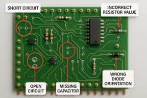
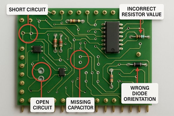
In-circuit testing (ICT) is an automated test that checks a populated PCB for manufacturing defects. It uses a "bed of nails" fixture to access individual nodes, detecting shorts, opens, incorrect component values (resistance, capacitance), missing components, and wrong component orientation for polarized parts like diodes and electrolytic capacitors.
As a hardware engineer, I've seen ICT save projects by catching defects early. It’s a powerful tool, but it's not a magic bullet. Understanding exactly what it can—and can't—do is key to using it effectively. This post will walk you through the details of ICT, from its core advantages to how it compares with other methods, helping you make smarter decisions about your testing strategy.
What Are The Main Advantages And Disadvantages Of ICT?
You need to test thousands of boards quickly, but functional testing is too slow and expensive for high-volume production. How do you ensure quality without creating a massive bottleneck and driving up costs?
The main advantage of ICT is its speed and high fault coverage for manufacturing defects, making it ideal for mass production. Its primary disadvantages are the high upfront cost for creating a custom test fixture and the lack of test access on increasingly dense board designs.

I've used ICT extensively on large-scale projects, like the Tuxedo Keypad at Honeywell. The initial investment in the fixture, which can range from a few thousand to over $20,000, was significant. However, the test itself takes about 30-60 seconds per board, compared to 5-10 minutes for a full functional test. When you're producing thousands of units, that time saving is enormous and provides a clear return on investment. The challenge is that without good test point access designed in from the start, the effectiveness of ICT drops dramatically.
Breaking Down the Pros and Cons of ICT
ICT is a strategic tool where the high initial capital expense is justified by lower per-unit test costs at scale. Its value is a direct function of production volume.
Key Advantages of In-Circuit Testing
- High Throughput: With test times of 30-60 seconds, an ICT machine can process 400-800 boards in an 8-hour shift. This speed is essential for keeping pace with modern, high-volume SMT assembly lines.
- Comprehensive Fault Coverage: ICT excels at finding the most common manufacturing flaws—shorts, opens, wrong parts, missing parts, and reversed parts. It typically achieves \(90\%-98\%\) coverage of these structural defects, providing high confidence that the board was assembled correctly.
- Simple, Actionable Diagnostics: When a board fails, the ICT system provides a clear, specific error message (e.g., "Short between net R1-1 and C5-2"). This allows a junior technician to perform diagnostics and repair, freeing up senior engineers for more complex tasks.
Key Disadvantages of In-Circuit Testing
- High Initial Cost and Inflexibility: The custom "bed of nails" fixture is the biggest hurdle. The cost depends on the board's node count and complexity, ranging from $5,000 for a simple, single-sided fixture to over $25,000 for a complex, dual-sided fixture with thousands of probes. Any layout change, even a minor one that moves a test point, requires a costly fixture modification or a completely new one.
- Requires Rigorous Design-for-Test (DFT): The board must be designed for testability from day one. This means adding hundreds of non-functional test pads, which consumes valuable board real estate. On dense, space-constrained designs, this can be a major challenge.
- Blind to Functional and Performance Issues: ICT confirms the board was built right, not that it works right. It won't catch firmware bugs, signal timing issues, or components that fail under operational load.
The Alternative for Prototypes: Flying Probe Testing
For prototyping and low-volume production, a Flying Probe Tester is an excellent alternative. It uses 4 to 8 robotic probes that move around the board to test points programmatically. Its pros include having no custom fixture needed, making it very flexible and cost-effective for small batches (\(<500 \text{ units}\)). The primary con is that it is much slower, with test times of 5-15 minutes per board, making it unsuitable for mass production.
| Feature | Flying Probe Tester | In-Circuit Tester (ICT) |
|---|---|---|
| Best Use Case | Prototypes, Low Volume (\(<500 \text{ units}\)) | High-Volume Production (\(>1000 \text{ units}\)) |
| Fixture Cost | None | High ($5,000 - $25,000+) |
| Speed per Board | Slow (5-15 minutes) | Fast (30-60 seconds) |
| Setup Time | Fast (hours) | Slow (weeks, for fixture fabrication) |
What Defects Are Undetectable By ICT?
Your boards are passing ICT, but you're still seeing field failures. Customers are reporting issues that your manufacturing tests should have caught, creating costly returns and damaging your reputation. What is the test missing?
ICT cannot detect functional or performance-related defects. This includes timing issues, firmware bugs, power integrity problems under load, signal integrity issues like crosstalk, and intermittent faults that only appear under specific thermal or operating conditions. It also misses non-electrical components.
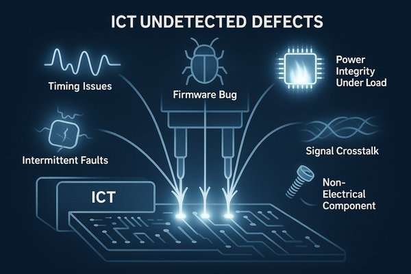
Early in my career, I worked on a board that consistently passed ICT but failed intermittently in the field. The problem was a signal integrity issue—crosstalk between two high-speed traces that only caused errors when the system was running at full clock speed. ICT powers the board but doesn't operate it at speed, so it never saw the problem. It confirmed all the resistors were the right value and nothing was shorted, but it couldn't tell us the design was flawed. This experience taught me that ICT is a structural test, not a functional one.
Examining the Blind Spots of In-Circuit Testing
ICT performs a static, DC, or low-frequency AC check of the board's components and connections. It does not simulate the board's actual operating environment. This fundamental difference is the source of its limitations.
Blind Spot 1: Functional and Parametric Failures
ICT tests components in isolation. It cannot verify that a DAC (Digital-to-Analog Converter) produces the correct analog voltage when given a specific digital code from the MCU. It can confirm a \(32.768 \text{ kHz}\) crystal is connected, but it cannot measure its frequency accuracy (e.g., \(\pm 20 \text{ parts per million}\)) or stability over temperature.
Blind Spot 2: High-Speed and Signal Integrity Defects
The test is blind to analog signal integrity issues like overshoot, undershoot, and ground bounce on high-speed digital lines. These defects can cause intermittent data corruption that only a high-speed oscilloscope or a functional test can catch.
Blind Spot 3: Power Integrity Problems Under Load
The test will verify that a \(3.3\text{V}\) power rail is not shorted to ground. It will not detect if that same rail experiences excessive voltage droop or ripple when a high-current component, like a processor, transitions from an idle to a full-load state.
Blind Spot 4: Hidden Physical and Intermittent Defects
While ICT can detect a completely open or shorted BGA pin (if connected to a test point), it cannot find subtle but critical defects like voids, micro-cracks, or "head-in-pillow" faults. A board might also have a component that only fails above \(50^{\circ}\text{C}\), an issue invisible to a standard ICT performed at room temperature.
The table below summarizes these blind spots and the proper tools to find them.
| Defect Category | Specific Examples | Recommended Test Method to Detect It |
|---|---|---|
| Functional Failures | Firmware bugs, incorrect component interaction, wrong logic | Functional Test (FCT) |
| Signal Integrity Issues | Crosstalk, overshoot, impedance mismatch, ground bounce | FCT with an oscilloscope, SI analysis |
| Hidden Solder Defects | BGA voids, "head-in-pillow," insufficient solder | Automated X-ray Inspection (AXI) |
| Intermittent Faults | Faults that appear with heat, cold, or vibration | FCT in an environmental chamber (HASS) |
Can ICT Test Digital And Programmed Components?
You have a complex board with microcontrollers and FPGAs. You know ICT is great for checking resistors and capacitors, but can it verify that these complex digital parts are soldered correctly and working?
Yes, ICT can test digital and programmed components, but in a limited way. It primarily performs static digital logic tests to check for solder joint defects (opens/shorts) on the component's pins and can be used to program blank devices like flash memory or microcontrollers.
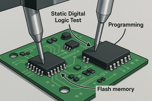
On the Tuxedo Keypad, we used ICT not just to check for manufacturing faults but also as the first step in our programming and provisioning process. The ICT fixture would first verify all the hardware was correct. If that passed, it would then use the same test points to flash the initial bootloader onto the main microcontroller via its JTAG or SWD interface. This combined step was incredibly efficient. It saved us from having a separate programming station and ensured we didn't waste time trying to program a board that had a hardware fault.
How ICT Tests and Programs Complex Components
Testing digital ICs with ICT moves beyond simple value measurements. It involves powered tests to check pin-level connectivity and often incorporates programming to streamline the manufacturing flow.
How ICT Performs Digital Logic and Vector Testing
This is a low-speed, static test to ensure the digital IC is alive and connected. The tester uses a pre-defined "vector file" to stimulate the IC's input pins with logic-level signals (e.g., \(0\text{V}\) for low, \(3.3\text{V}\) for high) and checks the response on the output pins. This process verifies the device's truth table at a basic level but does not test its AC performance or timing characteristics.
Using ICT for On-Board Programming (ISP)1
This feature transforms the ICT from just a tester into a manufacturing workstation. The ICT fixture connects to the device's programming interface (JTAG, SWD, ICSP, SPI, etc.) to load firmware after structural tests pass. This "Test and Program in One" approach is highly efficient, though programming speed may be slower than a dedicated gang programmer.
Unpowered Checks Using Internal Component Diodes
An unpowered test can check for shorts or opens by using the IC's internal ESD protection diodes. By biasing the chip's power rails, the tester can check the integrity of each pin's connection through these diodes without fully powering the device.
This table summarizes these digital test types:
| ICT Digital Test Type | Purpose | Key Limitations |
|---|---|---|
| Unpowered Diode Check | Verifies pin continuity and checks for shorts without powering the IC. | Cannot detect functional faults or open pins on outputs. |
| Powered Vector Testing | Checks for opens, shorts, and basic logic functionality (stuck-at faults). | Not an at-speed test; does not verify AC/timing performance. |
| On-Board Programming (ISP) | Loads firmware, bootloaders, or serial numbers onto programmable devices. | Can be slower than dedicated programmers; requires test access. |
How Does ICT Verify Component Values Like Resistance And Capacitance?
You've specified a \(10 \text{ k}\Omega\) precision resistor in your design, but a mix-up on the assembly line could place a \(1 \text{ k}\Omega\) resistor instead. How can you be sure the correct component values are on every board?
ICT verifies component values using a technique called a "guarded" measurement. The tester applies a known current (or voltage) to the component under test and measures the resulting voltage (or current), then calculates the value. Guarding isolates the component from parallel circuit paths.
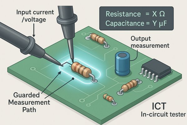
I remember debugging an amplifier circuit where the gain was completely wrong. The board had passed ICT, which was confusing. After digging in, we found that two resistors were in a parallel configuration that the ICT test program hadn't properly guarded against. The tester was measuring the combined parallel resistance, which fell within the tolerance of the target resistor. It was a lesson in the importance of a well-written test program. A simple measurement isn't enough; you have to actively isolate what you're measuring.
How Guarded Measurements Ensure Accuracy
On a populated PCB, components are interconnected, creating complex networks. The guarding technique electrically removes parallel "sneak paths" that would corrupt the measurement, often in combination with a 4-wire Kelvin setup2 for precision.
How ICT Measures Different Component Types
- Resistors: A DC current is forced, and DC voltage is measured. The value is calculated via Ohm's Law (\(R = \frac{V}{I}\)).
- Capacitors: An AC voltage at a known frequency (typically \(1 \text{ kHz}\)) is applied, and the resulting AC current is measured. The impedance is calculated, and from there, the capacitance is derived (\(C = \frac{1}{2\pi f Z}\)).
- Inductors: Similar to capacitors, an AC stimulus is used to measure impedance, from which inductance is calculated (\(L = \frac{Z}{2\pi f}\)).
This process is summarized below:
| Component Type | ICT Stimulus | What is Measured | Calculation Principle |
|---|---|---|---|
| Resistor | Known DC Current (e.g., \(1 \text{ mA}\)) | Resulting DC Voltage | Ohm's Law (\(R = \frac{V}{I}\)) |
| Capacitor | Known AC Voltage (e.g., \(1\text{V} \text{ @ } 1 \text{ kHz}\)) | Resulting AC Current | Impedance (\(C = \frac{1}{2\pi f Z}\)) |
| Inductor | Known AC Voltage (e.g., \(1\text{V} \text{ @ } 10 \text{ kHz}\)) | Resulting AC Current | Impedance (\(L = \frac{Z}{2\pi f}\)) |
Understanding the Limits of Guarding
While powerful, guarding has limits. It is less effective when trying to measure a high-impedance component (e.g., \(1 \text{ M}\Omega\)) in parallel with a very low-impedance one (e.g., \(100~\Omega\)). A skilled test engineer must recognize these situations and devise multi-stage tests.
Does ICT Verify Correct Component Orientation?
You're using polarized capacitors and diodes in your design. If one of these is installed backward, it could fail immediately upon power-up, potentially damaging other parts of the board. How do you catch this simple but critical assembly error?
Yes, ICT can verify the correct orientation of polarized components like diodes, electrolytic capacitors, and transistors. It uses specific electrical tests that measure the component's unique behavior in the forward and reverse directions to confirm it is placed correctly.
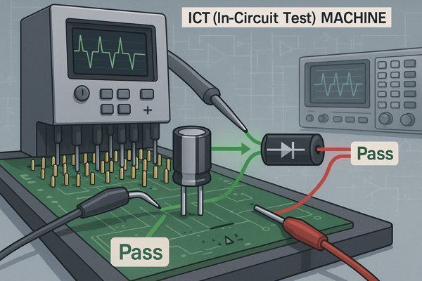
I once had a batch of boards for a medical device where a single tantalum capacitor was installed backward on a power rail. The board would seem fine at first, but after a few minutes, the capacitor would short, causing the power supply to fail. The functional test caught it, but not before wasting valuable time. After that, we added a specific orientation test to our ICT program. The test was simple: it checked for high resistance in the reverse direction. This immediately caught the assembly error on subsequent batches, saving us countless hours of debug and rework.
How ICT Electrically Verifies Component Placement
ICT does not use cameras; it deduces orientation based on a component's electrical asymmetry. The test method is tailored to the component type.
Checking Diode and Transistor Orientation
The tester performs a forward and reverse bias test. It applies a small positive voltage and expects to see current flow (\(\approx 0.7\text{V}\) drop for silicon), then reverses the voltage and expects to see almost no current flow. If the results are flipped, the part is reversed.
Verifying Polarized Capacitor Placement
A non-destructive leakage test is performed. A small DC voltage (\(1-2\text{V}\)) is applied in the correct polarity. A good, correctly installed capacitor will show very high resistance. If it's backward, it will conduct, showing a much lower resistance.
Detecting IC Rotation with Protection Diodes
Even without full power, ICT can often check orientation by testing the internal ESD protection diodes present on each I/O pin. By checking for these diodes relative to the VCC and GND pins, the tester can detect if an IC is rotated.
Here is a summary of these tests:
| Component Type | ICT Test Method | Pass Criteria (Correct Orientation) |
|---|---|---|
| Diode / LED | Forward & Reverse Bias Test | Low resistance forward, high resistance reverse. |
| Polarized Capacitor | Low-Voltage DC Leakage Test | Very high resistance (low leakage current). |
| IC | Unpowered ESD/Protection Diode Check | Correct diode presence detected between I/O pins and VCC/GND. |
How Does Automated Optical Inspection (AOI) Compare To ICT?
You're trying to decide on the right test strategy for your new product. You need to catch manufacturing defects, but you're not sure whether to invest in ICT, AOI, or both. Which one gives you the best return?
AOI is a visual inspection method that uses cameras to find defects, while ICT is an electrical test. AOI is faster to set up and excels at finding placement errors, whereas ICT is better for verifying component values and finding electrical shorts/opens.
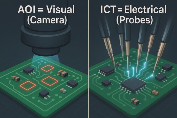
In my experience, AOI and ICT are complementary tools, not competitors. At Smiths Medical, we used both in our SMT line. AOI was placed "in-line" right after the reflow oven. It gave us real-time feedback, catching a tombstoned resistor moments after it happened. This allowed operators to adjust the pick-and-place machine immediately. The boards then went to ICT for "end-of-line" structural testing, which caught hidden electrical faults like wrong capacitor values. Using both gave us comprehensive coverage and a better process.
Comparing AOI and ICT: Strengths and Weaknesses
AOI: Visual Inspection Strengths and Weaknesses
- Strengths: AOI is fast to set up with no fixture cost. It excels at finding visual and quality defects like missing components, poor solder fillets, and polarity based on markings. Modern 3D AOI can even measure solder paste volume and component height. It's ideal for real-time process feedback.
- Weaknesses: AOI cannot verify electrical values—it can't tell a \(1\text{k}\) resistor from a \(10\text{k}\) resistor in the same package. It also has blind spots for joints hidden under components like BGAs.
ICT: Electrical Testing Strengths and Weaknesses
- Strengths: ICT provides a definitive electrical test, directly measuring component values and confirming connectivity. It can find hidden shorts under components that cameras cannot see.
- Weaknesses: ICT has a high setup cost due to the custom fixture. It cannot judge the quality of a solder joint, only that a connection exists. It is typically used at the end of the line, so feedback to the process is slow.
This table provides a quick summary:
| Feature | Automated Optical Inspection (AOI) | In-Circuit Test (ICT) |
|---|---|---|
| Test Principle | Visual (Camera-based) | Electrical (Probe-based) |
| Setup Cost | Low (Software setup) | High (Custom hardware fixture) |
| Finds Wrong Values? | No (can only read markings) | Yes (primary strength) |
| Finds BGA Defects? | No (blind to hidden joints) | Limited (only if pin has a test point) |
When Is Boundary Scan Testing Used Instead Of ICT?
Your board is packed with high-density components like BGAs and fine-pitch QFPs, leaving no room for traditional ICT test pads. How can you test for manufacturing defects when you can't physically probe the pins?
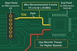
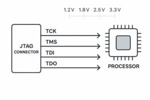
Boundary scan (JTAG) testing is used when physical test access is limited or impossible. It's a digital testing method that accesses the pins of compliant ICs through a simple four- or five-wire test port, without needing direct probe contact.
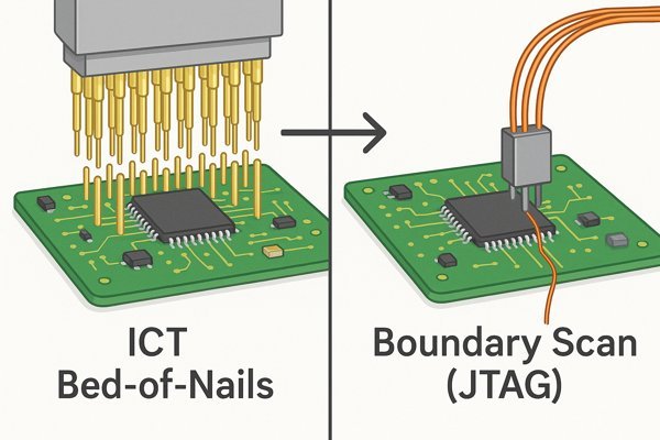
At Lightelligence, I worked on an evaluation board for a photonic computing chip. The board was incredibly dense, with multiple BGAs and high-speed connectors. Placing test pads for ICT was simply not an option. Instead, we relied heavily on boundary scan. By connecting to the JTAG port, we could verify the integrity of the connections between the main processor, the FPGA, and the memory chips. It allowed us to confirm that hundreds of BGA pins were correctly soldered down without a single test probe.
Boundary Scan: The Solution for Limited Test Access
Boundary scan, standardized as IEEE 1149.1 (JTAG), is a test architecture embedded within complex ICs. It provides a digital, non-contact method for testing PCB interconnects, making it indispensable for modern electronics. While both are used to find manufacturing defects, they are fundamentally different tools.
| Feature | In-Circuit Test (ICT) | Boundary Scan (JTAG) |
|---|---|---|
| Test Access | Requires physical access via test pads ("bed of nails") | Requires only a 4/5-pin TAP connector and compliant ICs |
| Component Coverage | Tests digital, analog, and passive components | Primarily tests interconnections between digital JTAG-compliant ICs |
| Cost | High fixture cost; lower test development cost | No fixture cost; potentially higher software/development cost |
| Ideal Use Case | High-volume boards with good test point access | High-density boards with many BGAs and limited physical access |
A hybrid ICT/Boundary Scan approach is often the best solution. The ICT fixture probes the analog, power, and connector sections, while the integrated boundary scan controller tests the dense BGA-to-BGA connections.
What Are The Best Practices For Design For Testability (DFT) For ICT?
You want to use ICT for your next project, but you know its success depends on the PCB layout. What specific design rules should you follow to ensure your board is fully testable and avoids problems during production?
The best practices for ICT Design for Testability (DFT) are to place test pads on every net, use standard pad sizes and spacing (e.g., \(1.0 \text{ mm}\) pads with \(2.54 \text{ mm}\) spacing), and include tooling holes for a precise board alignment in the fixture.
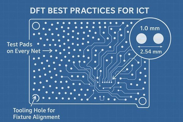
I've reviewed countless designs where DFT was an afterthought, and the consequences are always the same: reduced test coverage and painful compromises. On one project, the team had placed test points too close to tall components. When the ICT fixture was built, the probes couldn't make reliable contact without hitting the component's body. We had to accept a lower test coverage on that revision, a risk that could have been easily avoided by following basic DFT rules from the start.
A Practical Checklist for Test-Ready PCB Designs
Good DFT isn't just about adding pads; it's about making the testing process reliable, repeatable, and cost-effective.
The Golden Rule: One Test Point Per Net
This is the most critical principle to ensure 100% shorts coverage and is the foundation of a comprehensive ICT strategy.
Physical Layout Rules for Reliable Probing
- Single-Sided Probing: Place all test points on one side of the PCB (typically the bottom/solder side) to create a simpler, cheaper fixture.
- Dedicated Pads: Never use component pads or leads as test points. Solder on these surfaces is uneven and can cause poor contact.
- Even Distribution: Distribute test points as evenly as possible across the board to prevent the PCB from bowing under pressure from the probes.
Key Specifications for Test Pads and Tooling Holes
The table below summarizes key physical design rules.
| Parameter | Recommended Value (Metric) | Recommended Value (Imperial) | Reason |
|---|---|---|---|
| Test Pad Diameter | \(1.0 \text{ mm}\) | \(40 \text{ mils}\) | Provides a sufficient target for the probe. |
| Test Pad Spacing (Center) | \(\ge 2.54 \text{ mm}\) | \(\ge 100 \text{ mils}\) | Standard probe pitch; reduces fixture cost. |
| Clearance from Board Edge | \(\ge 3.0 \text{ mm}\) | \(\ge 125 \text{ mils}\) | Allows fixture clamps to hold the board without interference. |
| Tooling Hole Diameter | \(3.175 \text{ mm} (\pm 0.05 \text{ mm})\) | \(125 \text{ mils} (\pm 2 \text{ mils})\) | Standard size for precise alignment pins in the fixture. |
How Is An ICT Test Program Generated?
You've designed your PCB with excellent DFT, and the first prototypes are being assembled. Now, you need to create the actual test that will run on the ICT machine. What does that process involve?
An ICT test program is generated by processing the board's CAD data (e.g., ODB++) and Bill of Materials (BOM). This information is used to locate all the components and nets, create a fixture design, and automatically generate the basic test sequence.
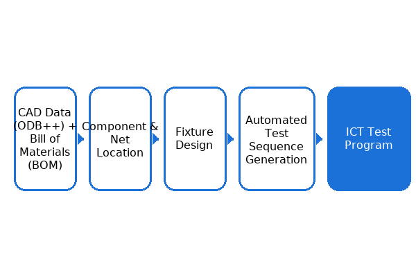
When I was the technical lead for the Tuxedo Keypad, generating the ICT program was a standardized process. We would release a package containing the final ODB++ files, the BOM, the schematic, and a netlist to our manufacturing partner. Their test engineers would feed this data into their ICT software. The software automatically generated about \(80\%\) of the test. The final \(20\%\) involved manual refinement by an experienced test engineer to optimize guarding and debug the fixture on a "golden" board.
From Design Files to a Finished Test Program
Creating a robust ICT test program is a systematic process that combines automation with expert engineering knowledge.
Step 1: Gathering the Required Design Data
A complete and accurate data package is the foundation. This includes intelligent CAD Data (like ODB++), a precise Bill of Materials (BOM) with tolerances, and the schematics.
Step 2: Automated Generation of the Baseline Program
The ICT system's software parses this data to build the test foundation. It generates the fixture design files and applies pre-written test modules from its library for standard components.
Step 3: Engineering Refinement and Validation
This is where automation ends and engineering skill begins. The test engineer reviews the auto-generated program, manually adds guard points, adjusts test tolerances, and develops any custom test scripts. The entire program is then validated against a known-good "golden" board.
| Step | Required Inputs | Key Activities & Outputs |
|---|---|---|
| 1. Data Preparation | CAD Data (ODB++, IPC-2581), BOM, Schematics | Engineer gathers and verifies all design files are final and consistent. |
| 2. Fixture & Program Generation | All data from Step 1 | Software parses data, maps test points, and generates fixture build files. Auto-generates basic tests. |
| 3. Refinement & Validation | Auto-generated program, Schematics, "Golden" board | Engineer adds guarding, sets tolerances, debugs false failures, and validates the final program. |
What Are The Common Causes Of False Failures In ICT?
Your production line is stopped because the ICT machine is flagging good boards as bad. This "false failure" problem is killing your efficiency, and you need to find the cause quickly. What usually goes wrong?
The most common causes of false failures in ICT are worn-out or dirty test probes causing poor contact, incorrect test tolerances, and fixture alignment issues. Environmental factors like static discharge or electrical noise can also cause intermittent, incorrect readings.
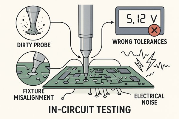
I remember a frustrating situation where a specific capacitor test started failing on \(30\%\) of our boards after a few months of production. It turned out that the test probe for that specific pad had become worn and contaminated with flux residue. After thousands of cycles, the contact resistance was just high enough to throw off the measurement. A simple probe cleaning and replacement fixed the issue instantly. It taught me that ICT is a physical, mechanical system, and it needs regular maintenance.
Identifying the Root Causes of False Failures
False failures (Type I errors) are insidious because they turn your quality control tool into a production bottleneck. They typically fall into three categories.
Cause 1: Physical Problems with the Fixture and Probes
This is the source of over \(80\%\) of false failures. Probes get dirty with flux residue or simply wear out after their rated cycle life (\(100\text{k}-500\text{k}\) actuations). Poor board alignment due to worn tooling pins can also cause intermittent contact.
Cause 2: Flaws in the Test Program and Tolerances
Setting test tolerances too tightly is a common mistake. The limits must account for both component tolerance and tester variance. Missing guard points or insufficient stabilization delays can also cause incorrect readings.
Cause 3: External Factors and Process Variation
A new batch of components might have a slightly different value distribution. Board warpage can prevent it from sitting flat in the fixture. ESD damage during handling can cause a real failure that appears random.
This table organizes the common causes and their solutions:
| Cause Category | Specific Cause | Common Solution(s) |
|---|---|---|
| Physical Fixture | Dirty or contaminated probes | Implement a regular probe cleaning schedule. |
| Worn out probes (exceeded cycle life) | Proactively replace probes based on actuation count. | |
| Test Program | Tolerances are too tight | Widen test limits; perform a statistical analysis (Cpk). |
| External Factors | Board warpage | Improve board manufacturing process or fixture clamping. |
How Can ICT Test Coverage Be Improved?
You're using ICT, but your report says you only have \(85\%\) test coverage. This means \(15\%\) of your board's connections are not being tested, creating a blind spot for potential defects. How can you close this gap?
ICT test coverage is improved primarily through better Design for Testability (DFT). This means adding test points to all electrical nets, ensuring adequate clearance around those points, and using boundary scan (JTAG) for high-density components where physical probing is impossible.
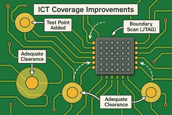
On a cost-reduction project for a legacy product, we were tasked with shrinking the board size. The first layout version came back with only \(70\%\) ICT test coverage because the engineers had removed many test points to save space. I had to reject the layout. We went back and found creative ways to add small test vias back into the design, eventually getting coverage up to \(95\%\). It was a classic trade-off: a slightly larger board was a small price to pay for the assurance that our products were being tested thoroughly.
A Three-Part Strategy for Maximum Test Coverage
Test coverage is the key metric for ICT effectiveness. Aiming for \(>95\%\) net coverage is a realistic goal for most designs and requires a combination of good design, smart tool usage, and continuous improvement.
Strategy 1: Implement a Rigorous DFT Plan
This is non-negotiable and has the biggest impact. The "one test point per net" rule is the most important principle.
Strategy 2: Augment ICT with JTAG and Flying Probe Testing
For modern, high-density designs, combine ICT with Boundary Scan (JTAG) to test components like BGAs where probes cannot go. During prototyping, use a Flying Probe tester to get high coverage before the DFT is finalized.
Strategy 3: Analyze and Act on Test Coverage Reports
Use the "uncovered nets" list from your ICT software as an action plan for the next PCB revision. Perform a risk analysis on each untested net to prioritize which ones must get a test point.
Here is a summary of strategies to improve coverage:
| Strategy | Key Action | Impact on Coverage |
|---|---|---|
| Design for Testability | Add a test point to every net ("100% access"). | The single most effective way to achieve maximum coverage. |
| Hybrid Testing | Integrate Boundary Scan (JTAG) into the ICT sequence. | Covers dense digital ICs (BGAs) where probes cannot go. |
| Test Coverage Analysis | Review the "uncovered nets" report from the ICT software. | Provides a specific, actionable list of gaps to address in the next design revision. |
What Is The Process For Debugging A Failing ICT Test?
A board has just failed ICT. The tester has printed out a ticket with a fault message like "Open circuit on net RESET_L." What is the step-by-step process a technician follows to find the cause and fix the board?
The process for debugging a failing ICT test starts with analyzing the tester's fault report. A technician then uses a multimeter and schematic to confirm the fault on the physical board, visually inspects the area for defects, and performs the necessary rework.
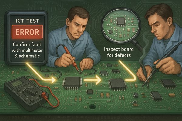
During my time at Honeywell, I saw our repair technicians handle thousands of ICT failures. Their process was incredibly systematic. First, they'd look at the failure log. Then, they would pull up the schematic and board view. With a multimeter, they would probe the exact pins identified by the ICT report to confirm the short or open. \(90\%\) of the time, the problem was a visible solder bridge or a dry joint, which they could fix in minutes. This fast feedback loop is what makes ICT so valuable in a production environment.
A Step-by-Step Guide to Debugging Failures
A skilled technician follows a structured process to ensure accurate and efficient diagnosis. This process prevents wasted time and avoids "shotgun" repairs where multiple components are replaced without a clear root cause.
The Debugging Workflow: From Report to Rework
The main steps are to analyze the report, confirm the fault on the bench, perform a close visual inspection under a microscope, and then rework the board. After the repair, the board must be re-tested to verify the fix.
Beyond the Single Board: Analyzing Trends with a "Bone Pile"
For high-volume manufacturing, technicians will periodically analyze the "bone pile" of failed boards. If they notice that the same component, R52, is consistently failing for an open circuit across dozens of boards, this indicates a systemic problem. It's not a random defect anymore; it could be a flaw in the solder paste stencil, a problem with the pick-and-place machine, or a bad batch of components. This higher-level analysis is crucial for improving overall production yield.
| Step | Tools Used | Objective / Goal |
|---|---|---|
| 1. Analyze Fault Report | ICT Test Log / Failure Ticket | Understand the type of fault and the specific components/nets involved. |
| 2. Confirm the Fault | Digital Multimeter (DMM), Schematic, Layout Viewer | Manually verify the fault on the bench. This rules out a false failure from the ICT fixture. |
| 3. Visual Inspection | High-Magnification Microscope | Find the physical root cause of the fault (e.g., solder bridge, cold joint). |
| 4. Rework & Re-Test | Soldering Station, ICT Machine | Correct the physical defect and verify the fix. |
Conclusion
In-circuit testing is a fast, powerful tool for catching manufacturing defects. By understanding its strengths, weaknesses, and how to design for it, you can make it a cornerstone of your production test strategy.


