
Poor impedance control in printed circuit boards (PCBs) leads to signal reflections, distortions, and EMI, causing severe performance issues in high-speed digital and RF circuits. These problems can result in unreliable communication, data corruption, or complete system failure. Without careful design, impedance mismatches become the hidden culprits of PCB malfunctions. This guide equips engineers with the necessary knowledge to eliminate these issues by mastering PCB impedance control and ensuring reliable circuit performance.
Introduction
What is PCB Impedance Control, and Why is it Important?
PCB impedance control is the process of maintaining a controlled impedance range for signal traces to minimize reflections and signal degradation. In high-speed and RF PCB design, ensuring consistent impedance helps preserve signal integrity, reduce data loss, and mitigate electromagnetic interference (EMI).
What Real-World Problems Arise from Poor Impedance Control?
- Signal Integrity Issues: Data corruption from reflections, ringing, and signal degradation in high-speed and RF circuits.
- EMI: Increased radiation and signal leakage, severely impacting RF and high-speed digital applications.
- Crosstalk: Unwanted coupling between traces causing noise, degrading performance in high-speed digital routing.
- Reduced Reliability: Instability in high-speed and RF signals, leading to malfunctioning circuits and degraded system performance.
Fundamentals of PCB Impedance
What is Impedance, and How Does It Differ from Resistance?
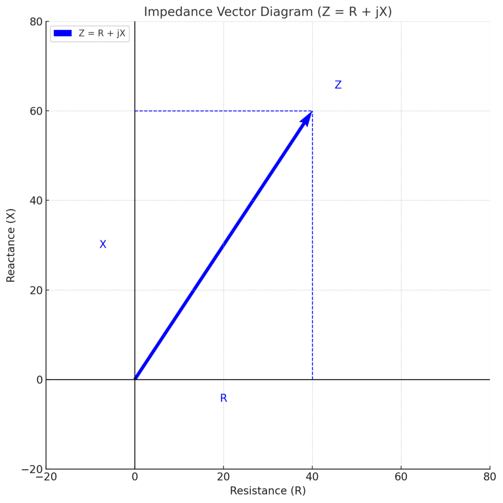
Impedance (Z) is the total opposition to AC current, consisting of resistance (R) and reactance (X). It is mathematically defined as:
\( Z = R + jX \)
where:
R (Resistance): A frequency-independent component that dissipates energy as heat.
X (Reactance): A frequency-dependent component that includes inductive reactance \( X_L \) and capacitive reactance \( X_C \), given by:
\( X = X_L – X_C \)
Inductive Reactance:
\( X_L = 2\pi f L \)
Increases with frequency \( f \).
Capacitive Reactance:
\( X_C = \frac{1}{2\pi f C} \)
Decreases with frequency \( f \).
Unlike resistance, impedance varies with frequency, making it crucial in high-speed and RF PCB designs to prevent signal reflections and maintain signal integrity.
How Do Capacitance, Inductance, and Resistance Influence Impedance?
- Capacitance: Affects impedance by storing and releasing energy between conductors, increasing reactance at high frequencies.
- Inductance: Opposes changes in current flow, increasing impedance as frequency rises.
- Resistance: Dissipates energy as heat and remains constant regardless of frequency.
Why Do High-Frequency Signals Require Controlled Impedance?
At high frequencies, PCB traces function as transmission lines, meaning they exhibit distributed capacitance and inductance, which impact signal speed, cause reflections, and can lead to signal attenuation or distortion if impedance is not properly controlled.
How Does Impedance Impact Signal Transmission, Distortion, and Reflections?
Signal Transmission: Impedance affects signal propagation in PCB traces by controlling how voltage and current interact. When impedance is matched, signals travel with minimal distortion and power loss, ensuring efficient transmission. If impedance varies, it can lead to energy reflections, signal attenuation, or phase shifts, impacting overall circuit performance.
Distortion: Mismatched impedance alters signal waveforms, causing overshoot, undershoot, and ringing. These distortions affect data accuracy and can lead to errors in high-speed circuits.
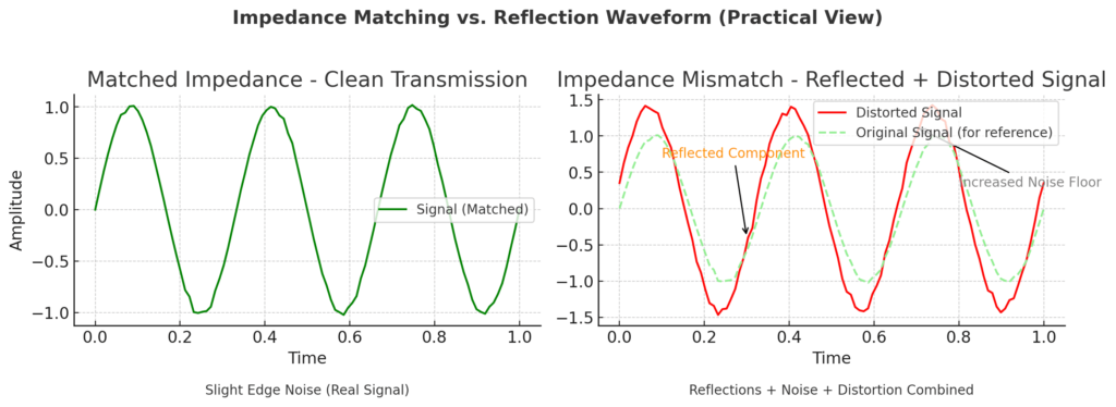
Reflections: When impedance mismatches occur, part of the signal is reflected back toward the source, interfering with the original signal. This results in standing waves, increased EMI, and reduced transmission efficiency.
Understanding Different Impedance Types
What is Characteristic Impedance, and Why Does It Matter?
Characteristic impedance Z0 is the inherent impedance of a PCB trace when treated as a transmission line. It is defined by:
$$
Z_0 = \sqrt{\frac{L}{C}}
$$
where:
- L = Inductance per unit length (H/m)
- C = Capacitance per unit length (F/m)
Why It Matters:
Characteristic impedance must be carefully controlled in high-speed and RF circuits to prevent signal reflections and transmission losses. Proper impedance matching ensures efficient energy transfer and minimizes waveform distortion.
What is Single-Ended Impedance, and When Is It Used?
Single-ended impedance applies to signals transmitted over a single PCB trace with a reference to a ground plane. It is given by:
$$
Z_{single} = \sqrt{\frac{L}{C}}
$$
Use Cases:
- Low-speed digital signals
- General-purpose PCB traces
- RF applications where single-ended transmission is practical (e.g., antenna feeds)
What is Differential Impedance, and Why Is It Essential for High-Speed Signals?
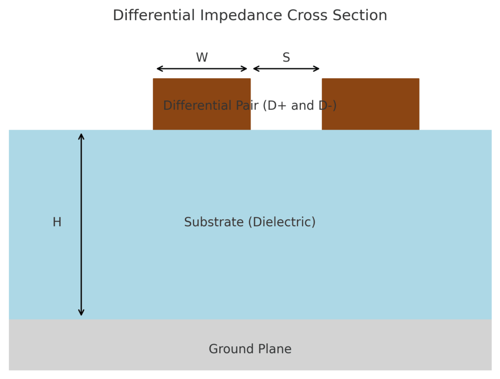
Differential impedance Zdiff applies to a pair of traces carrying equal and opposite signals. It is defined as:
$$
Z_{diff} ≈ 2Z_0 (1 – k)
$$
where k is the coupling coefficient between the traces.
Importance:
Differential signals reduce EMI, improve noise immunity, and enhance signal integrity, making them essential for high-speed protocols such as USB, HDMI, PCIe, and Ethernet.
What Are the Key Differences Between Single-Ended and Differential Traces?
| Feature | Single-Ended Impedance | Differential Impedance |
|---|---|---|
| Signal Type | One conductor & ground | Two complementary signals |
| Noise Immunity | Lower | Higher (common-mode noise rejection) |
| EMI Emission | Higher | Lower (due to balanced signals) |
| Use Case | General PCB traces | High-speed serial interfaces |
What is Common-Mode Impedance, and How Does It Affect EMI?
Common-mode impedance Zcm refers to the impedance experienced when both traces in a differential pair carry the same voltage relative to ground. It is defined as:
$$
Z_{cm} = \frac{V_{cm}}{I_{cm}}
$$
where:
- Vcm = Common-mode voltage (V)
- Icm = Common-mode current (A)
High common-mode impedance can cause EMI issues, as noise is radiated instead of being canceled out. Proper PCB design techniques, such as reducing trace asymmetry and adding common-mode chokes, help mitigate these effects.
Effect on EMI:
If common-mode noise is not controlled, it can interfere with nearby circuits, leading to compliance failures in EMC testing.
Factors That Influence PCB Impedance
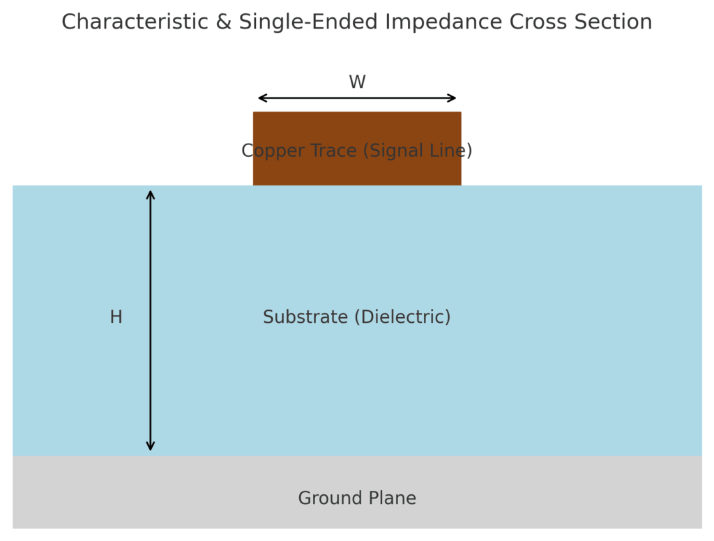
How Does Trace Width Affect Impedance?
Wider traces lower impedance. This is because wider traces have more surface area facing the reference plane, allowing stronger electric fields to form, which increases capacitance (C). Capacitance per unit length:
C ∝ w / h
Higher capacitance reduces impedance, following:
Z₀ ∝ 1 / √C
Since trace width (w) directly increases capacitance, the relationship simplifies to:
Z₀ ∝ 1 / w
- Wider trace = Higher capacitance = Lower impedance
- Narrower trace = Lower capacitance = Higher impedance
Why Does Trace Spacing Matter in Controlled Impedance?
For differential pairs, spacing directly affects electromagnetic coupling between the two traces. Wider spacing reduces coupling, increasing Zdiff. The approximate formula is:
Zdiff ≈ 2Z₀(1 – k)
where:
- Z₀ = Characteristic impedance of each individual trace
- k = Coupling coefficient, which increases as spacing decreases
Smaller spacing increases k, reducing Zdiff. Larger spacing reduces k, increasing Zdiff.
What Role Does Distance from the Reference Plane Play?
The distance between a trace and its reference plane (h) directly affects capacitance and therefore impedance. The relationship is:
C ∝ 1 / h
Closer traces have stronger electric fields between the trace and plane, increasing capacitance. Since:
Z₀ ∝ 1 / √C
Higher capacitance reduces impedance, so:
Z₀ ∝ h
- Smaller h (closer trace) = Higher capacitance = Lower impedance
- Larger h (further trace) = Lower capacitance = Higher impedance
Controlling trace height in stack-up design is critical for achieving accurate impedance, as even small variations in h during manufacturing can significantly shift final impedance.
How Does the Dielectric Constant (Dk) of PCB Materials Affect Impedance?
The dielectric constant (Dk) describes how much the PCB material can store electrical energy. It directly influences capacitance between the trace and reference plane. The relationship is:
C ∝ Dk
Since characteristic impedance relates inversely to the square root of capacitance:
Z₀ ∝ 1 / √Dk
- Higher Dk increases capacitance, lowering impedance.
- Lower Dk decreases capacitance, raising impedance.
Choosing the right PCB material is crucial because different materials have different Dk values, and these values can vary with frequency.
What is the Effect of Copper Thickness on Impedance?
Thicker copper increases capacitance by enlarging the trace surface area facing the reference plane, enhancing electric field coupling. The relationship is:
C ∝ t
where t = copper thickness. Since:
Z₀ ∝ 1 / √C
More capacitance from thicker copper lowers impedance. Thinner copper reduces capacitance and raises impedance.
How Does PCB Stack-Up Design Influence Impedance?
Stack-up defines trace-to-plane distance, dielectric thickness, and layer order, all of which affect capacitance, inductance, and impedance. It also controls the proximity of signals to their reference planes and adjacent signal layers, influencing crosstalk and coupling. Proper stack-up ensures stable impedance, minimizes interference, and improves signal integrity.
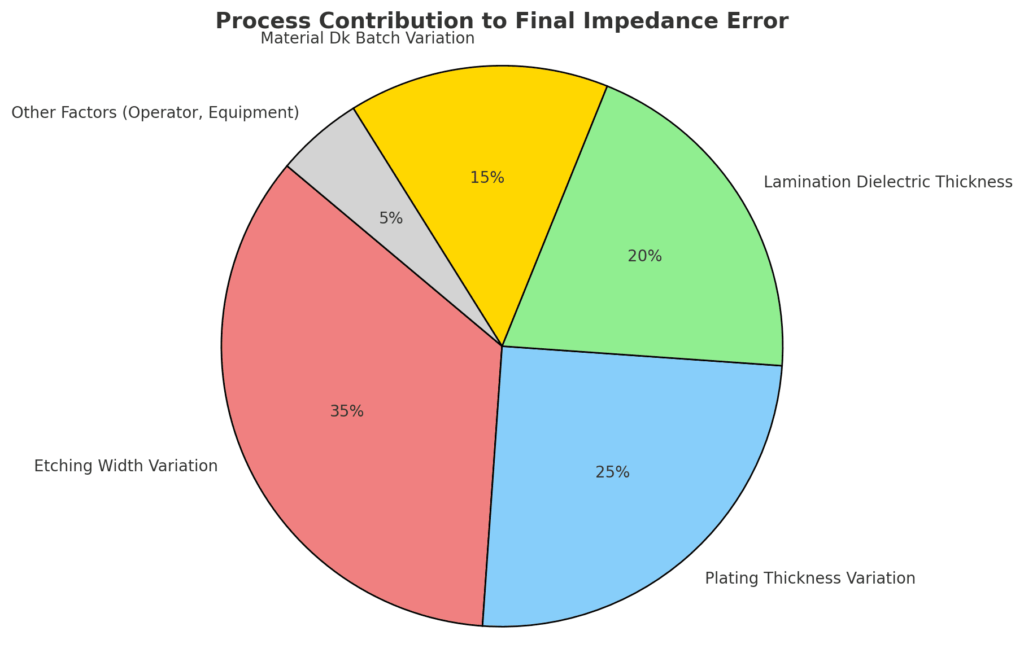
How Does PCB Manufacturing Tolerance Affect Final Impedance Values?
PCB manufacturing processes introduce multiple sources of impedance variation, all of which must be controlled to achieve the target impedance.
Etching Variation: During etching, actual trace width can deviate from design intent due to over-etching (narrower traces) or under-etching (wider traces). These changes directly alter impedance, since:
Z₀ ∝ 1 / w
Copper Thickness Tolerance: Copper thickness can vary across the panel and between fabrication runs. Since capacitance increases with copper thickness:
C ∝ t
and Z₀ ∝ 1 / √C, thickness variation shifts impedance.
Dielectric Thickness Variation: The actual spacing between signal layers and reference planes can differ from the intended design, directly affecting capacitance and impedance:
C ∝ 1 / h
Dielectric Constant (Dk) Variation: Even within the same PCB material type, the actual Dk can vary slightly across the panel or between material batches. Since:
Z₀ ∝ 1 / √Dk
This material variation also causes impedance drift.
Copper Surface Roughness: Rougher copper increases effective inductance and reduces effective capacitance, especially at high frequencies (due to skin effect), raising impedance.
Plating and Finish: Surface finishes such as ENIG can add thin layers of nickel and gold to traces, subtly affecting trace dimensions and surface conductivity. This has a minor effect at lower frequencies but becomes more important at GHz speeds.
Combining these factors, tight control over all manufacturing processes is critical to maintaining the specified impedance and ensuring consistent electrical performance across the final PCB.
Signal Integrity & Impedance Matching Techniques
What is Signal Integrity, and Why is it Tied to Impedance?
Signal integrity refers to the ability of a signal to travel through a PCB trace without excessive distortion, loss, or noise. Impedance directly affects signal integrity because mismatched impedance causes signal reflections, leading to waveform distortion and data errors.
What Happens When Impedance is Mismatched?
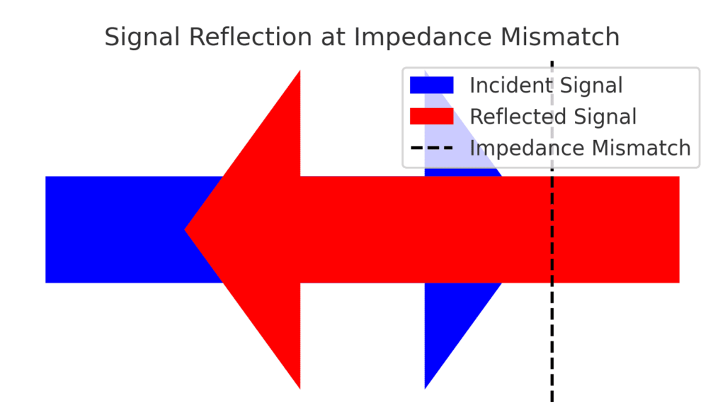
When a signal encounters an impedance mismatch at a junction (e.g., between trace and load), part of the signal reflects back toward the source. These reflections interfere with the original signal, degrading the quality.
Why Does Impedance Mismatch Cause Signal Reflections and Distortion?
Reflections happen when a signal encounters a point where impedance changes suddenly, creating a discontinuity. This disrupts smooth transmission and causes part of the signal to reflect back toward the source.
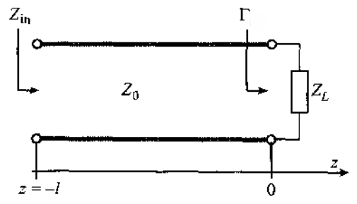
The amount of reflection is described by the reflection coefficient (Γ), defined as:
Γ = (Zₗ – Z₀) / (Zₗ + Z₀)
Where:
Zₗ = Load impedance
Z₀ = Characteristic impedance
How Γ behaves in different cases:
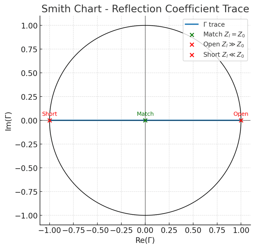
- If Zₗ = Z₀ (perfect match), Γ = 0 — no reflection, full signal transfer.
- If Zₗ ≫ Z₀ (open circuit), Γ approaches +1 — almost full reflection, same polarity.
- If Zₗ ≪ Z₀ (short circuit), Γ approaches -1 — almost full reflection, inverted polarity.
The greater the impedance mismatch, the larger the reflection, leading to stronger distortion and worse signal integrity.
How Does Impedance Mismatch Affect High-Speed Digital Signals?
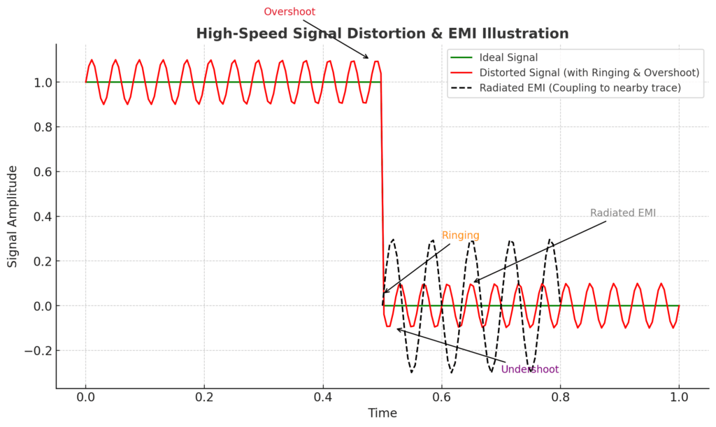
At high speeds, signals behave like fast edges rather than continuous waves. Reflections caused by impedance mismatches overlap with the main signal, causing:
- Ringing, overshoot, and undershoot.
- Data timing errors.
- Increased jitter (timing instability).
- Inter-symbol interference (ISI), where reflections from previous bits interfere with current bits.
- Higher electromagnetic emissions (EMI) due to radiated reflections.
- Noise coupling into power and ground planes, affecting other nearby signals.
These combined effects degrade signal integrity, reduce noise margins, and can cause data errors, especially in high-speed circuits.
What are the Most Common Impedance Matching Techniques?
Different termination techniques apply to different scenarios in PCB design:
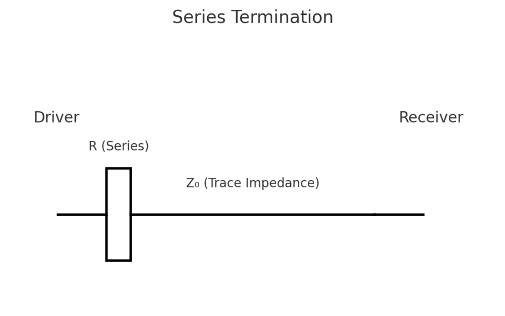
- Source Termination: This method matches the driver output impedance to the trace impedance. One common way to achieve this is through:
- Series Termination: A resistor is placed in series with the driver output so that the combined driver impedance and resistor match the trace impedance. This is highly effective in point-to-point unidirectional connections, especially for short and moderate trace lengths. It also helps reduce overshoot and ringing by damping fast edges.
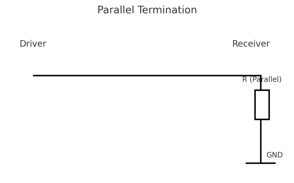
- Load Termination: This matches the impedance at the receiver (load) end of the trace to absorb reflections and prevent them from propagating back down the line. One important form of load termination is:
- Parallel Termination: A resistor placed at the receiver end to ground or to a reference voltage, providing continuous impedance matching. This is typically used in high-speed clock lines and differential pairs where maintaining constant impedance at the termination is crucial. Parallel termination consumes DC power continuously, making it less desirable in low-power designs.
Each termination method is selected based on signal type, directionality, trace length, speed, and power constraints. Correct choice and placement of termination resistors is critical to ensuring impedance matching and preserving signal integrity.
How Do Termination Resistors Help in High-Speed PCB Designs?
Termination resistors absorb reflected energy, preventing it from propagating back into the signal path. They also:
- Provide impedance matching between trace and load to ensure smooth signal transfer.
- Dampen fast edges, reducing overshoot, undershoot, and ringing.
- Stabilize signal waveforms to improve signal integrity.
- Reduce electromagnetic emissions (EMI) by minimizing standing waves.
- Improve noise margins, ensuring cleaner signal reception at the receiver.
Termination resistors are crucial in high-speed designs where signal quality must be preserved.
How Do PCB Layout Techniques Minimize Impedance Mismatches?
- Maintain consistent trace width and spacing to keep characteristic impedance stable.
- Control trace-to-plane distance through proper stack-up to maintain target impedance.
- Avoid sharp corners and sudden trace width changes, as they create localized impedance discontinuities.
- Minimize unnecessary via transitions to avoid sudden impedance changes at via locations.
- Avoid creating stubs during layout, as they act as resonators and cause reflections. Back-drilling, a fabrication process, is used to remove unused via stubs that remain after drilling through-vias, especially in high-speed designs.
- Ensure high-speed traces always route over continuous reference planes to maintain constant reference capacitance. Avoid crossing plane splits, which cause impedance discontinuities.
- Follow strict length matching and controlled spacing rules for differential pairs to preserve consistent differential impedance.
- Use controlled impedance design rules and impedance calculators such as Polar Si9000, Saturn PCB Toolkit, or AppCAD to design traces that match the target impedance at both the source and the load.
Careful layout combined with correct termination and manufacturing process control ensures signal integrity and minimizes distortion in high-speed and RF circuits.
Practical PCB Design for Controlled Impedance
How Do You Define Target Impedance Values?
Defining target impedance values requires balancing design requirements, signal performance, manufacturing capability, and compliance with industry standards.
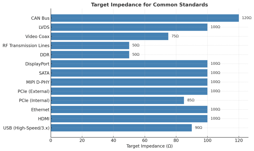
For high-speed digital and RF interfaces, industry standards provide clear target values to ensure interoperability across systems. Key standards include:
- USB (High-Speed/USB 3.x): 90Ω differential — specified to match USB cable impedance and ensure proper signal integrity.
- HDMI: 100Ω differential — standardized to match HDMI cable pairs, ensuring compatibility and low reflection.
- Ethernet: 100Ω differential — designed to match twisted-pair cabling, minimizing signal distortion and maintaining signal balance.
- PCIe: 85Ω or 100Ω differential — 85Ω for PCB routing inside devices; 100Ω for external cable interfaces.
- MIPI D-PHY: 100Ω differential — used in mobile camera and display links, matching typical flex cable impedance.
- SATA: 100Ω differential — required for SATA link reliability and compliance.
- DisplayPort: 100Ω differential — set to match DisplayPort cabling.
- DDR Memory Interfaces: Typically 50Ω single-ended — selected to balance impedance matching and signal integrity for memory bus performance.
- RF Transmission Lines: Typically 50Ω single-ended — standardized in RF systems to maximize power transfer and minimize mismatch losses.
- Video Coax (e.g., analog video transmission): 75Ω single-ended — the standard for video broadcast and home coaxial networks.
- LVDS (Low Voltage Differential Signaling): 100Ω differential — common in display, industrial, and sensor interfaces.
- CAN Bus (Controller Area Network): 120Ω differential — defined for twisted-pair wiring in automotive and industrial networks to maintain signal integrity over long runs.
For other general-purpose traces, such as low-speed control signals, analog sensor traces, and power distribution lines, impedance is not dictated by standards but driven by practical design goals:
- Power Traces: Minimize impedance to reduce voltage drop, improve power integrity, and reduce DC losses.
- Analog Traces: Match impedance to external components (e.g., sensor outputs, amplifier inputs, filter networks) to optimize signal transfer and prevent standing wave effects.
- Long Digital Traces: For lower-speed signals, controlled impedance may still be needed if the trace length exceeds ~1/10 the signal wavelength (based on rise time), to avoid ringing and reflections.
For clock signals, controlled impedance reduces jitter and reflections, ensuring stable timing margins. In mixed-signal designs, impedance matching of analog traces also helps minimize reflections and maintain signal fidelity, especially in noise-sensitive circuits.
In real-world engineering, experienced designers combine standard target values with custom tuning based on stack-up capabilities, trace length, expected noise environment, and component input/output impedance to define practical target impedance for each class of signal.
What are the Best Practices for Trace Routing in Impedance-Controlled Designs?
- Follow impedance calculators such as Polar Si9000, Saturn PCB Toolkit, or AppCAD to determine required trace width and spacing.
- Route over continuous reference planes to ensure stable capacitance and a smooth return path. Reference planes act as the return current path for high-speed signals. If the plane is split or discontinuous, the return current is forced to detour, increasing loop inductance and degrading both impedance control and EMI performance.

- Minimize via usage to avoid unnecessary discontinuities. Each via introduces localized capacitance and inductance, which alters impedance. If vias are necessary, ensure they transition between layers that share the same reference plane.
- Avoid sharp corners; use smooth bends or chamfered angles. Sharp corners change the effective trace width locally, creating sudden impedance jumps.
- Maintain consistent trace width along the entire path to keep impedance uniform.
- Ensure proper spacing between adjacent traces to minimize crosstalk, particularly for parallel high-speed traces.
- Ensure consistent reference plane type (GND to GND or PWR to PWR) across layer changes to avoid impedance discontinuities.
- Control return current path by avoiding gaps or voids in the reference plane beneath high-speed traces. Disrupted return paths increase noise and degrade signal integrity.
- Completely avoid stubs in layout as stubs act as resonant structures, causing reflections and impedance mismatches. When stubs are unavoidable, such as in through-vias used in multi-layer PCBs, apply back-drilling to remove unused via sections and minimize their impact on impedance.
- Length tune timing-critical signals such as differential pairs and memory buses to match propagation delays and maintain timing margins.
- Use via stitching near differential pairs, reference plane edges, and layer transitions to preserve continuous return paths and reduce mode conversion or unwanted radiation.

- Leverage controlled impedance rule enforcement directly in CAD tools to automatically apply width and spacing rules based on the selected stack-up.
- Account for impedance discontinuities at connectors, test points, and component pads, especially for high-speed interfaces.
- Consider solder mask effects for very high-frequency signals, as the presence or absence of solder mask alters the effective dielectric constant.
- Consult with fabricator early to align on achievable impedance tolerances, accounting for copper roughness, etching tolerances, and laminate variation.
Combining these layout techniques with careful stack-up design, accurate modeling, and clear communication with the manufacturer ensures reliable impedance-controlled PCB designs.
How Should Differential Pairs Be Routed to Maintain Correct Impedance?
- Matched Lengths: Differential pairs should aim for closely matched electrical lengths to maintain timing balance between the two signals. Electrical length accounts for propagation delays caused by different materials or stack-up layers. In practice, achieving “exactly the same length” is not realistic. Instead, designers set a length matching tolerance (e.g., within 5 mils for high-speed signals), balancing manufacturability and performance.
- Constant Spacing: Maintain uniform spacing between the pair along its entire length to ensure stable differential impedance. Any variation in spacing directly changes the impedance.
- Route over the same reference plane: Ensure both traces see the same plane type (GND or PWR) and, if possible, the same plane material and copper roughness to avoid skew caused by propagation velocity differences.
- Avoid unnecessary via transitions: Each via creates localized impedance change. If vias are required, both traces should transition together and symmetrically, maintaining matched geometries and equal electrical length through the via stack.
- Control coupling strength by optimizing spacing relative to trace width: Spacing directly controls differential impedance. The optimal spacing is derived from impedance calculations based on the selected stack-up, but designers must also consider crosstalk immunity when other signals are nearby. A common guideline is to maintain at least 3 times the trace width (3W rule) between a differential pair and adjacent signals to reduce unwanted coupling and preserve signal integrity.
Combining these techniques ensures that differential pairs meet both impedance and timing requirements, preserving signal integrity.
How Do Designers Use Simulation Tools & Calculators for Impedance Verification?
- Pre-Layout: Use impedance calculators such as Polar Si9000, Saturn PCB Toolkit, or AppCAD to determine correct trace width and spacing for the target impedance.
- Post-Layout: Use full-wave electromagnetic (EM) simulation tools such as Ansys HFSS, Keysight ADS, or Siemens HyperLynx to verify that actual layout geometry achieves the required impedance.
- Stack-Up Validation: Simulate the selected stack-up (layer thickness, materials) using tools like Polar Speedstack, Z-zero Z-planner, or directly in the above EM tools, to confirm the stack-up supports the required impedance.
What Are the Common Challenges and Mistakes in Designing for Controlled Impedance?
- Inaccurate Stack-Up Information: More than 60% of impedance deviations in real projects stem from using outdated or assumed stack-up data instead of confirming actual parameters with the PCB manufacturer.
- Ignoring Manufacturing Tolerances: Fabrication tolerances typically cause trace width to shrink by 0.5-1 mil during etching, and dielectric thickness can vary by ±10%. These variations directly shift the final impedance.
- Improper Trace Geometry: Sharp corners, uneven widths, and inconsistent differential pair spacing introduce localized impedance spikes. These discontinuities lead to reflections, degraded eye diagrams, and signal integrity loss.
- Routing Over Split Planes: When controlled impedance traces cross plane splits or voids, the return current is forced to detour, causing impedance jumps of up to 20-50%, depending on frequency.
- Underestimating Coupling and Crosstalk: In dense layouts, tight spacing between neighboring traces creates unintended coupling, reducing effective impedance by several ohms and increasing noise.
- Lack of Post-Layout Verification: More than 30% of impedance failures in production occur because post-layout electromagnetic simulation was skipped, leaving via effects, pad geometries, and localized discontinuities unaccounted for.
- Inconsistent Documentation and Communication: Nearly 25% of fabrication delays stem from unclear or contradictory stack-up data, impedance tables, and design files provided to the manufacturer.
- Multiple Trace Widths for Same Impedance: Specifying inconsistent widths for the same impedance target on a given layer causes confusion during fabrication, requiring clarification that slows production.
- Overly Tight Tolerances: Specifying unrealistic impedance tolerances (e.g., ±2%) increases manufacturing cost by 15-20% and can exceed practical process capability, especially in standard FR4 boards.
- Overlooking Solder Mask Effects: Removing or omitting solder mask changes the effective dielectric constant by around 0.1 to 0.2, shifting impedance by 2-4Ω at high frequencies.
- Ignoring Back-Drilling for Via Stubs: Unused via stubs can act as resonant elements, degrading signal quality by up to 30% at higher frequencies. Back-drilling removes these stubs and helps maintain consistent impedance.
Successful controlled impedance design requires clear documentation, early collaboration with the fabricator, strict layout discipline, and comprehensive post-layout verification to ensure the fabricated board meets both design intent and practical manufacturing tolerances.
Manufacturing and Quality Control Considerations
How Do You Communicate Impedance Requirements to a PCB Manufacturer?
Clear and precise communication is essential to achieve correct impedance during manufacturing. Designers should provide:
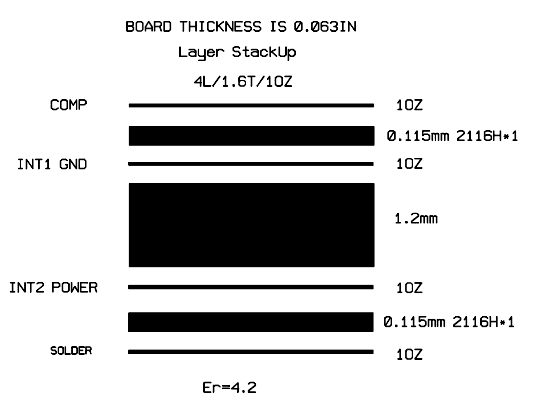
- Detailed Stack-Up Drawing: Specify material type, layer thickness, and copper weight. This stack-up should be confirmed with the fabricator before finalizing design.
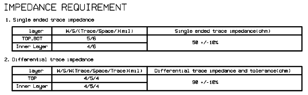
- Impedance Table: List all controlled impedance traces, their target values (e.g., 50Ω single-ended, 100Ω differential), and the layer they are on.
- Fabrication Notes: Clearly document controlled impedance nets and requirements in the fabrication drawing or notes accompanying the Gerber or ODB++ files.
- Tolerance Requirements: Specify realistic tolerances, typically ±10%, unless tighter control is critical.
In most cases, impedance requirements are communicated through external documentation (stack-up drawing, impedance table, fabrication notes). In some workflows using advanced formats like ODB++ or IPC-2581, certain impedance attributes (such as target impedance, single-ended or differential mode, and layer assignment) can also be embedded in the manufacturing data.
What Are the Typical Tolerances for Controlled Impedance in PCB Production?
- Standard Tolerance: ±10%, meaning a 50Ω trace would be acceptable between 45Ω and 55Ω. This is suitable for most digital designs and general high-speed applications.
- Tighter Tolerance: ±5%, meaning the same 50Ω target allows 47.5Ω to 52.5Ω. This tighter control is necessary for more demanding high-speed or RF applications and requires enhanced process control.
- Ultra-High Precision: Below ±5% is rare and typically reserved for RF, microwave, aerospace, and medical applications. Achieving this level requires specialized materials (e.g., PTFE or high-performance laminates), real-time process monitoring, and advanced quality control steps.
How Do Fabrication Processes Affect Final Impedance Values?
- Etching Process: Reduces trace width slightly, typically by 0.5-1 mil depending on copper thickness. Sidewall tapering (trapezoidal profile) further changes the effective width seen by high-frequency signals, subtly increasing capacitance.
- Lamination and Pressing: Slightly alters dielectric thickness across the panel. Variations in glass weave density cause localized Dk shifts, especially for differential pairs and high-speed traces that run diagonally across the weave.
- Plating Process: Adds copper to the trace, increasing width and thickness. Plating is often less uniform near panel edges due to current density distribution, meaning center and edge traces may have slightly different impedance.
- Material Variations: Actual dielectric constant (Dk) can vary ±5-10% for standard FR4, but high-frequency laminates (e.g., Rogers) typically control Dk within ±2-3%. Designers should also check the Df (dissipation factor), which impacts loss, especially above 5 GHz.
Combined Effects:
- Final impedance depends on the cumulative impact of all these factors. For example, ±0.5 mil etch tolerance plus ±10% dielectric variation can shift impedance by 5-10Ω in a typical high-speed design. This combined effect highlights why designers should work closely with the fabricator and use realistic tolerances instead of assuming ideal data.
Cost vs. Performance Trade-offs in PCB Impedance Control
How Do Different PCB Materials Impact Both Cost and Performance?
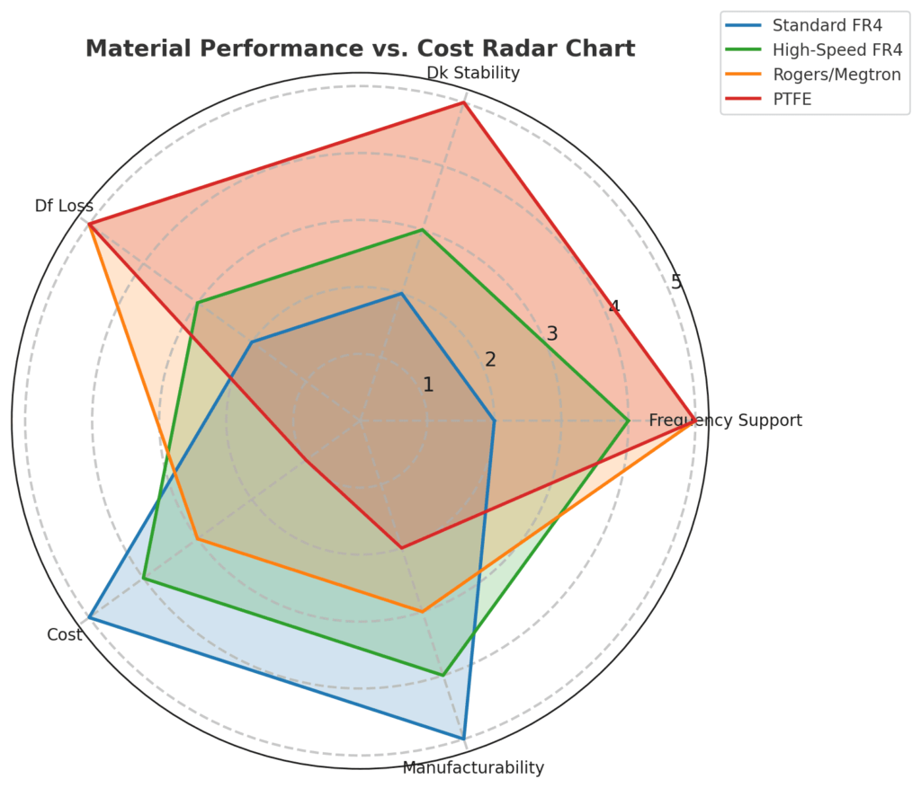
- Standard FR4: Low cost, sufficient for lower-frequency designs (<1 GHz) and less demanding impedance control.
- High-Speed FR4: Moderate cost, better suited for digital designs up to several GHz, with improved Dk consistency.
- Low-Loss Laminates (e.g., Rogers, Megtron): Higher cost, essential for RF, microwave, and very high-speed digital designs requiring tight impedance and low loss.
- PTFE-based Materials: Highest cost, used for microwave, millimeter-wave, and aerospace applications, providing ultra-stable Dk and extremely low loss.
How Can Designers Balance Cost, Manufacturability, and Impedance Accuracy?
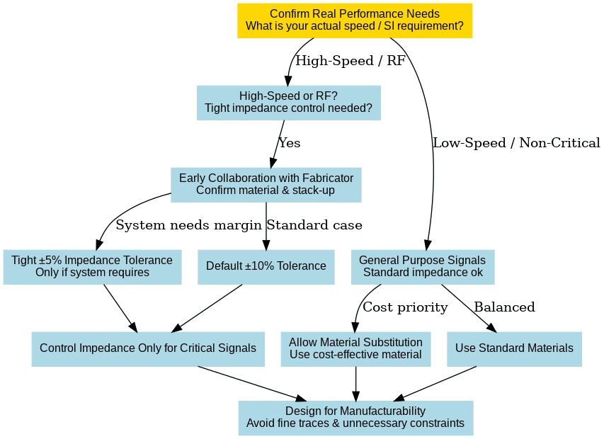
- Start with realistic performance needs: Over-specifying tight tolerances or exotic materials adds unnecessary cost.
- Collaborate with the fabricator early: Confirm stack-up, materials, and achievable tolerances upfront.
- Optimize stack-up for manufacturability: Use materials already stocked by the fabricator to reduce lead time and cost.
- Use standard impedance tolerances where possible: ±10% is achievable and cost-effective for most designs.
- Only request tight tolerances where analysis shows real need: Over-specifying ±5% or tighter should be justified by high-speed simulation or system requirements.
- Minimize layer count where possible: More layers increase complexity and cost.
What Are the Most Cost-Effective Strategies for Achieving Controlled Impedance?
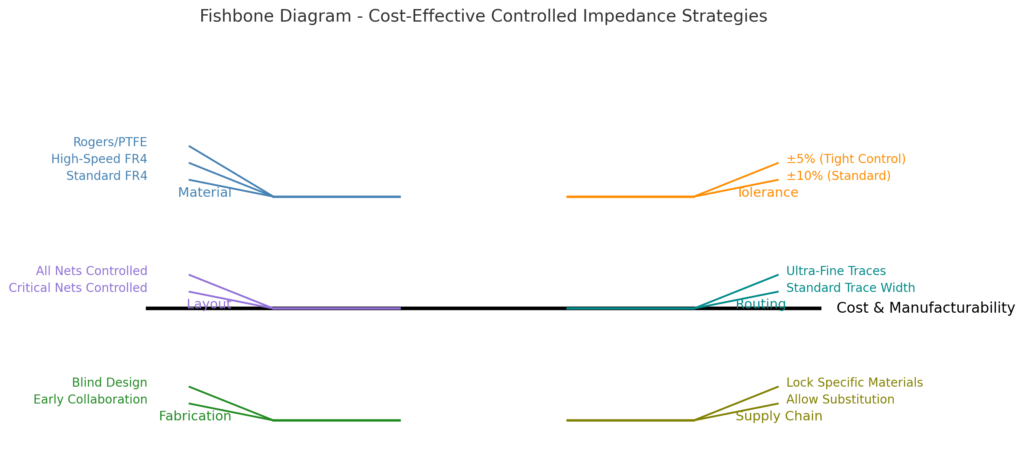
- Use proven standard stack-ups: Leverage well-characterized materials and structures that fabricators have experience with.
- Specify realistic tolerances: ±10% works for most applications, unless extreme precision is truly required.
- Limit the number of impedance-controlled traces: Only apply impedance control where signal integrity analysis shows it’s critical.
- Optimize trace geometry for manufacturability: Avoid ultra-fine traces unless necessary, as they are harder to control during etching.
- Allow flexible material selection: If exact materials are not critical, allow the fabricator to recommend cost-effective alternatives that meet performance needs.
Balancing these factors helps achieve reliable impedance performance without unnecessary cost inflation, keeping the design both technically sound and economically viable.
Summary
Controlled impedance is essential for signal integrity in high-speed and RF PCB designs. It depends on precise control of trace geometry, stack-up, materials, and reference planes. Successful impedance control requires collaboration between designers and fabricators, combining accurate pre-layout calculation, disciplined layout execution, and post-layout verification.
Designers must account for manufacturing tolerances and specify realistic requirements that balance performance and cost. Clear documentation — including stack-up drawings, impedance tables, and fabrication notes — is crucial for achieving intended impedance during manufacturing.
Mastering these processes allows engineers to predictably control impedance, ensuring reliable performance in demanding applications like high-speed digital interfaces, RF circuits, and modern communication systems.


