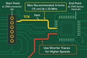
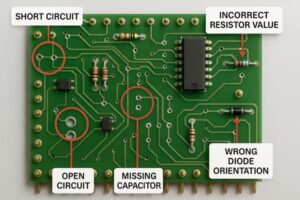
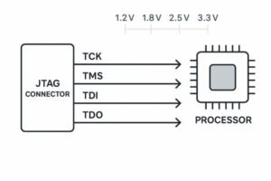
Programming a custom PCB often feels like the final, simple step. But many projects stumble here because they missed early critical planning. This oversight can lead to frustrating delays and even costly board redesigns. My approach, "Design for Programmability," treats this as a core part of the design from day one.
The key to programming a custom PCB is planning for it from the very start of your design. This means selecting appropriate microcontrollers, designing accessible programming interfaces (like JTAG or SWD headers), and ensuring your layout supports easy connection for flashing firmware and debugging.
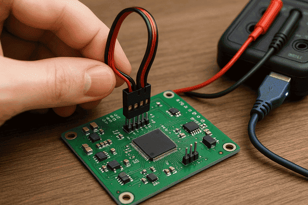
This article isn't just about plugging in a programmer. It's about a mindset shift. I've seen too many projects where the programming header was an afterthought, squeezed into a tight corner, making life difficult later. We need to think about how we'll talk to our creations right from the beginning. This ensures a smoother journey from design to a fully functional, programmable board. Let's explore how to get this right.
Can I learn PCB design on my own?
Feeling overwhelmed by PCB design? You see complex boards and wonder if it's possible to learn without formal training. The good news is, with the right resources and dedication, you absolutely can master it.
Yes, you can learn PCB design on your own. Many successful engineers are self-taught, using online courses, books, community forums, and practice projects. Start with basic circuits, understand component datasheets, and gradually tackle more complex designs.

I remember when I first started. The amount of information seemed huge. But I broke it down. First, I focused on understanding schematics – how components connect logically. Then, I moved to PCB layout, learning how to translate that schematic into a physical board. It takes time and consistent effort. You can start with simple projects, like a basic LED flasher circuit, and gradually increase complexity. The key is hands-on practice. Building something, even if it doesn't work perfectly the first time, teaches you invaluable lessons. Don't be afraid to make mistakes; they are part of the learning process. Many online communities are very supportive of beginners.
Here's a breakdown of key areas and resources:
| Area of Focus | Key Concepts | Recommended Resources |
|---|---|---|
| Schematic Capture1 | Symbols, netlists, logical connections | "The Art of Electronics" by Horowitz & Hill, KiCad/Eagle tutorials, component datasheets |
| Component Selection | Footprints, electrical parameters, cost, availability | Datasheets, supplier websites (Digi-Key, Mouser), Octopart |
| PCB Layout | Component placement, trace routing, layers, Design for Manufacturability (DFM), signal integrity | IPC-2221 (Generic Standard on Printed Board Design), EDA software tutorials, manufacturer design guides |
| Design Software (EDA) | EDA tool workflow, generating manufacturing outputs | KiCad (free, open-source), Autodesk Eagle (free/paid options), Altium Designer (professional, paid) |
| Prototyping & Test | Gerber/drill files, soldering techniques, debugging tools (multimeter, oscilloscope) | YouTube tutorials (e.g., EEVblog), Hackaday, SparkFun/Adafruit guides |
Learning on your own is a journey. It truly takes dedication, but seeing your own design come to life is incredibly rewarding.
Does PCB design require coding?
Many engineers starting out wonder if they need to be expert coders to design PCBs. This confusion can be a barrier. The truth is, the core activity of PCB design is distinct from coding, though they often go hand-in-hand in a complete product.
No, PCB design itself (schematic capture and layout) does not typically require coding. However, the microcontrollers or FPGAs placed on the PCB will need to be programmed using languages like C, C++, or HDL, which is a separate development activity.
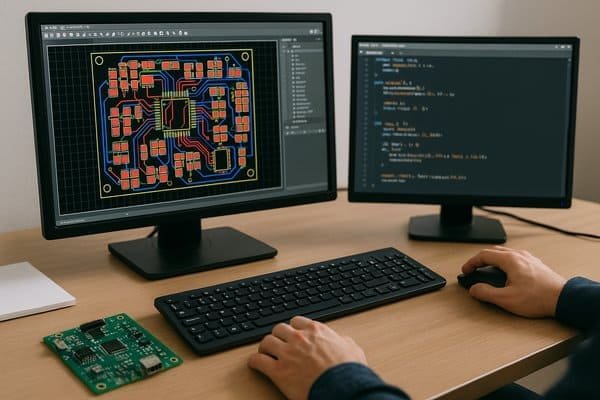
When I'm designing a PCB, my focus is on the electrical and physical aspects. This means working with graphical EDA (Electronic Design Automation) tools to place components like resistors (e.g., an 0603 package, which is 1.6mm x 0.8mm) or complex ICs, and then routing the copper traces that connect them. I'm considering things like signal integrity2 to prevent noise, power distribution to ensure all parts get stable voltage, and thermal management3. For instance, ensuring adequate copper plane area for heat dissipation for a power component. It's very much an engineering design task. The coding comes in when we need to tell the "brain" of the PCB—often a microcontroller or an FPGA—what to do. This is a distinct but related skillset.
Here's a table clarifying the differences:
| Aspect | PCB Design (Schematic & Layout) | Component Programming (MCU/FPGA) |
|---|---|---|
| Primary Activity | Graphical design of physical board, component placement, routing traces | Writing code/logic to define behavior of active components |
| Tools Used | EDA Software (Altium Designer, KiCad, Autodesk Eagle) | IDEs (e.g., STM32CubeIDE, MPLAB X, VS Code with PlatformIO), Compilers, Debuggers |
| Skills Required | Electrical engineering principles, DFM, SI/PI understanding | Software development, algorithm design, hardware interaction understanding |
| Output | Gerber files, BOM, Pick-and-Place data, Manufacturing documentation | Firmware (e.g., .hex, .bin files), FPGA bitstreams (.bit) |
| Is Coding Involved? | Generally no, but scripting (e.g., Python, AutoLISP-like languages in some EDA tools) for task automation is possible. | Yes, extensively (e.g., C, C++, Verilog, VHDL, MicroPython) |
At Honeywell, for the Tuxedo Keypad, my hardware design work was separate from the firmware team's coding, but our collaboration was constant to ensure the hardware perfectly supported all software features and vice-versa.
What software is used to design PCBs?
Choosing the right software for PCB design can feel like navigating a maze with so many options available. You want a tool that fits your needs and budget. The key is to find one that allows you to efficiently translate your ideas into a manufacturable design.
Popular PCB design software includes Altium Designer, KiCad, Autodesk Eagle, and OrCAD. The choice depends on factors like project complexity, budget (some are free, others expensive), and specific feature requirements like simulation or high-speed design capabilities.
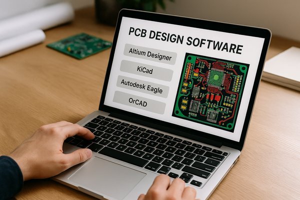
Over my nearly 20 years in embedded systems, I've used several EDA (Electronic Design Automation) tools. Each has its place, and the "best" one often depends on the specific project or company environment. For instance, a simple 2-layer board for a hobby project has very different software needs than a 12-layer board with multiple BGA components and 50-ohm controlled impedance traces for DDR memory, which might require advanced simulation tools integrated into the EDA suite. For those high-speed design4s, you're looking at trace length matching within, say, +/- 2.5 mils (0.0635mm) for critical signals.
Here's a comparative look at some common options:
| Software | Typical Cost | Target User | Key Strengths | My Experience Note |
|---|---|---|---|---|
| Altium Designer | $$$$ (Thousands USD per seat/year) | Professionals, Corporations | Comprehensive, high-speed design, 3D modeling, collaboration, extensive libraries | My go-to for complex industrial projects. |
| KiCad5 | Free (Open Source) | Hobbyists, Students, Small Businesses, Professionals | Powerful, cross-platform, large active community, no licensing cost, improving features | Excellent starting point, increasingly capable for professional work. |
| Autodesk Eagle | $ (Free limited version; Subscriptions from ~$15/month to ~$500/year) | Hobbyists, Makers, Small Businesses | Popular historically, good for smaller projects, large number of existing libraries | Many older open-source hardware projects were designed in Eagle. |
| OrCAD (Cadence) | $$$$ (Thousands USD per seat/year) | Professionals, Large Corporations | Advanced PSpice simulation, enterprise-level integration, robust for very complex PCBs | Seen in aerospace and large medical device companies for its rigor. |
| PADS (Siemens EDA) | $$$ (Subscription or perpetual, varies) | Professionals, Mid-to-Large companies | Strong for specific design needs, good balance of features and usability | Another solid professional tool I've encountered. |
My advice? If you're starting out, download KiCad. It's incredibly powerful for a free tool and will teach you all the fundamental concepts of schematic capture and PCB layout effectively.
What language is used to program PCBs?
You've designed your PCB, it's assembled, and now you need to bring it to life. What language do you use? This can be confusing because the PCB itself isn't programmed, but the active components on it are.
Microcontrollers on PCBs are most commonly programmed using C or C++. Assembly language is used for very low-level optimization or bootloaders. For FPGAs, Hardware Description Languages (HDLs) like VHDL or Verilog are standard.
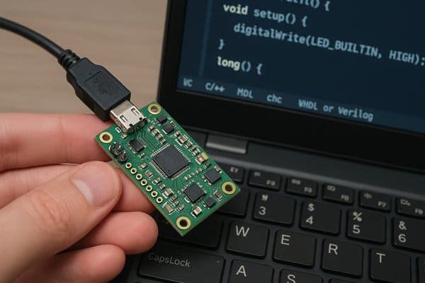
The "PCB" is the physical platform. The intelligence comes from the integrated circuits, primarily microcontrollers (MCUs) or Field-Programmable Gate Arrays (FPGAs), that are soldered onto it. The choice of programming language is dictated by these components and the project's requirements. For example, if you need real-time performance6 with minimal overhead for a motor control application on a Cortex-M4 MCU, C would be a very common choice. If you're designing a custom high-speed data acquisition interface with an FPGA, you'd use an HDL. It's about picking the right tool for the specific job the silicon needs to perform.
This table summarizes the common languages and their uses:
| Language | Target Component | Typical Use Cases | Pros | Cons |
|---|---|---|---|---|
| C | Microcontrollers (MCUs)7 | Firmware, device drivers, real-time operating systems (RTOS), low-level hardware interaction | Highly efficient, precise hardware control, widely supported by vendors, small code size | Manual memory management, can be complex for large projects, prone to pointer errors |
| C++ | Microcontrollers (MCUs) | More complex embedded applications, systems requiring object-oriented design | Abstraction, code reusability (classes, inheritance), better for large-scale projects | Can lead to larger code size/memory footprint if not used carefully, steeper learning curve than C |
| Assembly Language | Microcontrollers (MCUs) | Bootloaders, highly performance-critical routines, specific hardware initialization | Maximum control over hardware, highest possible speed for specific tasks | Processor-specific (not portable), very difficult to write and debug, error-prone |
| VHDL / Verilog (HDLs)8 | FPGAs, CPLDs | Custom digital logic design, parallel processing, high-speed interfaces, signal processing | True hardware parallelism, deterministic timing, ideal for tasks software can't handle | Different paradigm from software programming (describing hardware), steep learning curve, verbose |
| MicroPython/CircuitPython | Microcontrollers (MCUs) | Rapid prototyping, education, hobbyist projects, IoT devices where development speed is key | Easy to learn (Python syntax), fast development cycle, many available libraries | Slower execution speed and higher memory usage compared to C/C++, not suitable for all real-time tasks |
For most of my career developing embedded systems, C has been the predominant language for programming the MCUs on the boards I've designed, offering the best balance of control and performance.
How to create a custom PCB?
Creating a custom PCB can seem like a big undertaking, with many steps from idea to physical board. You might worry about missing something crucial. The process is systematic, though, and breaking it down makes it manageable.
Creating a custom PCB involves defining requirements, schematic design, component selection, PCB layout, generating manufacturing files (Gerbers, BOM), prototyping, and iterative testing/debugging. Prioritizing Design for Manufacturability (DFM) and Design for Programmability (DFP) throughout is key.
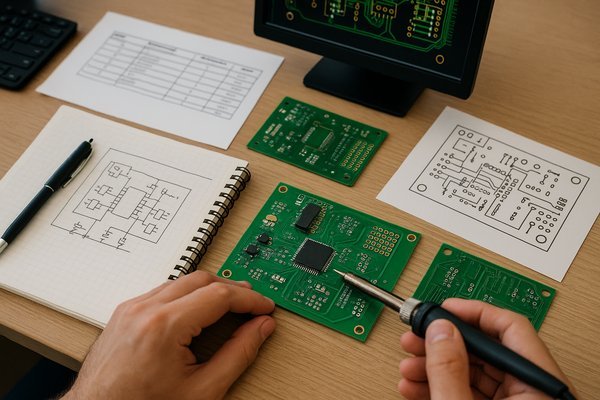
I've led many projects from initial concept to mass production, and the core steps are always similar. It starts with a clear understanding of what the PCB needs to achieve. This includes not just functionality but also constraints like size (e.g., must fit a 50mm x 30mm enclosure), cost (target BOM cost under $10), and power consumption (e.g., operate for 1 year on a CR2032 coin cell). My "Design for Programmability" philosophy means considering how the firmware will be loaded and debugged right from this initial stage. For instance, deciding whether to use a 6-pin SWD connector (approx. 5mm x 2.5mm footprint) or a more complex JTAG interface.
Here's a typical workflow I follow, with a focus on DFM in layout:
-
Concept & Requirements: Define functionality, performance, size, cost, programming/debug strategy.
-
Schematic Design: Create the circuit diagram in EDA software.
-
Component Selection: Choose parts considering specs, cost, footprint, availability.
-
PCB Layout: Physical board design.
- DFM (Design for Manufacturability9): This is crucial. You must design according to your chosen manufacturer's capabilities. IPC-2221B10 is a good general standard, but always get specific DFM rules from your fab house.
Parameter Typical Budget Manufacturer Advanced Manufacturer IPC-2221B (Level B - Standard Producibility) Example* Min. Conductor Width (Trace) 0.127mm (5 mil) < 0.075mm (3 mil) 0.15mm (external, up to 1oz copper), 0.1mm (internal) Min. Conductor Spacing 0.127mm (5 mil) < 0.075mm (3 mil) 0.15mm (external), 0.1mm (internal, varying with voltage) Min. Via Hole Diameter (Finished) 0.3mm (12 mil) < 0.15mm (6 mil) ~0.2mm for 1.6mm board thickness (aspect ratio dependent) Min. Via Annular Ring 0.127mm (5 mil) < 0.075mm (3 mil) 0.05mm + plating allowance (e.g., total ~0.1mm-0.15mm) Note: These are illustrative. Always confirm specific capabilities with your chosen PCB manufacturer. IPC values can vary based on many factors.
-
Generate Manufacturing Files: Gerbers, Drill files, BOM, Pick & Place.
-
Prototyping & Assembly: Order a small batch (3-5 boards).
-
Bring-up & Testing: Flash firmware, test functionality, debug.
-
Iteration: Revise if needed.
This systematic approach, especially emphasizing DFM and DFP early, significantly reduces risks and improves project outcomes.
What are the specific steps to program a custom PCB?
Your custom PCB is designed and assembled, but now the crucial part: getting your firmware onto it. This can feel like a black box. Without clear steps, you might face connection issues or failed uploads, which is incredibly frustrating when you're so close to seeing your project work.
To program a custom PCB, connect a programming tool (like a J-Link or ST-Link) to the board's programming interface (e.g., SWD/JTAG), use programming software to select your compiled firmware file (e.g., a .hex or .bin file), and then flash it to the microcontroller.
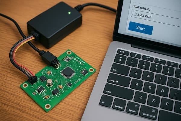
Having a reliable programming setup is essential. I remember early in my career, struggling with intermittent JTAG connections11 on a complex aerospace board. It turned out to be a noisy ground on the programming adapter. Once fixed, programming became smooth. The specific steps involve preparing your firmware, connecting the right hardware, using the correct software utility, and then loading the code. It's a methodical process, and getting it right ensures your carefully designed hardware actually does what it's supposed to do.
Here's a more detailed breakdown of the typical steps involved:
| Step | Key Action(s) | Tools & Interfaces Involved | Common Pitfalls & Tips |
|---|---|---|---|
| 1. Preparation | Compile firmware, select/obtain programmer, install drivers. | IDE (e.g., STM32CubeIDE, MPLAB X), Compiler (e.g., GCC, XC8), Programmer (e.g., Segger J-Link, ST-Link, PICkit), USB drivers. | Using firmware compiled for the wrong MCU architecture. Ensure programmer compatibility with your specific MCU. J-Link, for example, supports a wide range of ARM cores and some RISC-V. |
| 2. Software Setup | Install and configure programming utility software. Select target MCU and programming interface/speed. | Programming Utility (e.g., J-Flash, STM32CubeProgrammer, MPLAB IPE, OpenOCD). | Selecting the wrong device in the software. For interface speed (e.g., SWD clock), start low (e.g., 100 kHz - 1 MHz) and increase if stable. Max SWD speed can be 10-50 MHz for some MCUs/programmers. |
| 3. Hardware Connection | Power up custom PCB. Connect programmer to PCB's programming header (e.g., SWD, JTAG, ICSP). | PCB, Power Supply (e.g., 3.3V or 5V), Programming Cable, Programming Header (e.g., 10-pin ARM Cortex Debug Connector - 1.27mm pitch, or a 6-pin ICSP header). | Incorrect pinout alignment (check VCC, GND, SWDIO, SWCLK, nRST carefully!). Poor connections. Powering the target with the wrong voltage. Ensure programmer and target share a common ground. |
| 4. Establish Communication | Use programming utility to connect to/detect the target MCU. | Programming Utility. | "Cannot connect to target" errors. Check all physical connections, power, clock signals, and ensure the MCU is not held in reset or in a deep sleep mode. |
| 5. Flash Firmware | Erase MCU flash (optional but recommended). Select compiled firmware file (e.g., .hex, .bin). Program/Download. Verify (optional but recommended). | Programming Utility. | Forgetting to erase old firmware. Flashing to an incorrect memory address. Verification failures can indicate signal integrity issues on programming lines or faulty flash. |
| 6. Disconnect & Test | Disconnect programmer. Reset MCU (if not done automatically). Observe PCB behavior to test new firmware. | Custom PCB. | MCU does not start (check reset circuitry, power, external oscillator if used). Firmware bugs. |
Following these steps methodically will significantly increase your success rate when programming your custom PCBs. Always double-check your connections and software settings before hitting "program."
Conclusion
Successfully programming a custom PCB hinges on early planning and thoughtful design. Integrating programmability from the start, not as an afterthought, saves immense time and frustration down the line.
-
Understanding Schematic Capture is crucial for creating effective electronic designs; this resource will deepen your knowledge. ↩
-
Learn about techniques to maintain signal integrity in your designs, crucial for reliable electronic performance. ↩
-
Understanding thermal management is vital for preventing overheating in your designs; explore effective strategies here. ↩
-
Understanding high-speed design challenges can help you choose the right tools and techniques for your projects. ↩
-
KiCad is a powerful free tool; this resource will guide you through its features and help you start designing effectively. ↩
-
Discover techniques for achieving real-time performance in embedded systems, crucial for applications like motor control. ↩
-
Explore this link to understand the role of MCUs in embedded systems and their diverse applications. ↩
-
Learn about VHDL and Verilog to grasp how they enable custom digital logic design and parallel processing in FPGAs. ↩
-
Understanding DFM is crucial for optimizing PCB production and ensuring quality. Explore this link to enhance your knowledge. ↩
-
IPC-2221B provides essential guidelines for PCB design. Learn more to ensure your designs meet industry standards. ↩
-
Understanding JTAG connection issues can help you troubleshoot and ensure a smooth programming process. ↩


