 Skip to content
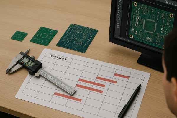
Stuck waiting for parts? Delays in PCB delivery can derail your entire project. Understanding typical lead times helps you plan better and meet your deadlines.
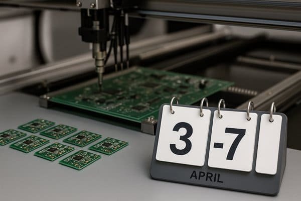
A standard PCB prototype (2-4 layers) typically takes 3-7 working days for fabrication. More complex boards (6+ layers, special materials, or finishes) can take 7-15 working days. Mass production timelines extend to 2-6 weeks, depending on volume and complexity.

Understanding the factors that influence PCB lead times is crucial for any hardware engineer. From design complexity to manufacturing capabilities and even shipping logistics, each step plays a part. I've navigated these timelines for nearly two decades, from rapid prototypes for aerospace to high-volume consumer electronics at Honeywell. Let's break down the common questions I hear about PCB timelines and costs, so you can manage your projects more effectively. This knowledge will keep your projects on track and help you avoid costly delays.
How Much Does PCB Design Cost Per Hour?
Worried about ballooning design costs? Unclear hourly rates can make budgeting a nightmare. You need transparent pricing to manage your project expenses effectively.
PCB design services typically range from $50 to $150 per hour. Junior designers or freelancers might charge at the lower end, while experienced engineers or specialized design firms can charge $100 to $150+ per hour, especially for complex high-speed or RF designs.

The cost of PCB design isn't just a number; it's an investment in your product's success. When I was leading the hardware design for a next-generation infusion pump at Smiths Medical, we carefully evaluated design service costs against the expertise required. The complexity of integrating sensors, signal processing, and motor control demanded seasoned engineers, and their rates reflected that. Trying to cut corners here often leads to more expensive revisions later. The hourly rate for PCB design can vary significantly based on several factors detailed below. At Honeywell, for the Tuxedo Keypad, we often leveraged senior designers for critical RF sections, even if their hourly rate was higher, because their efficiency and ability to foresee problems saved money in the long run. Understanding these nuances helps in selecting a design partner whose costs align with your project's technical demands and budget. It's not just about the cheapest rate, but the best value for the required expertise.
| Factor | Description | Typical Impact on Rate |
|---|---|---|
| Designer's Experience1 | Specialized skills (high-speed, RF, medical compliance) command higher rates. | Higher |
| Design Complexity2 | Simple 2-layer vs. complex 12-layer with controlled impedance, DDR4, etc. | Higher for complex |
| Location of Designer/Firm | Rates vary by region due to cost of living and market demand (e.g., North America/Western Europe vs. Asia/Eastern Europe). | Varies |
| Tools and Software Used | Proficiency in high-end EDA tools (Cadence Allegro, Mentor Xpedition, Altium with advanced simulation) can influence rates. | Higher for advanced |
How Long Does PCB Design Take?
Is your project timeline tight? PCB design can be a bottleneck if not planned properly. Knowing the typical duration helps you set realistic schedules.
A simple 2-layer PCB design might take 1 to 3 days. A moderately complex 4-6 layer board can take 1 to 2 weeks. Highly complex designs (e.g., 8+ layers, high-speed interfaces) can take 3 to 6 weeks or even longer.
The time it takes to design a PCB is one of the most common questions I get, and the answer is always "it depends." I recall working on the PACE evaluation board for Lightelligence; that was an extremely complex board with a photonic computing chip. The design phase, even with a dedicated team, took several weeks due to the novel technology and stringent signal integrity requirements3. It's not just about placing components and routing traces; it's about ensuring the design meets all functional, performance, and manufacturability requirements. Several key elements contribute to the overall PCB design timeline, and iteration cycles can add to this. Effective project management and clear requirements upfront are key to minimizing delays.
| Design Stage | Simple Design (e.g., <50 comp.) | Moderate Design (e.g., 50-200 comp.) | Complex Design (e.g., >200 comp., high-speed) |
|---|---|---|---|
| Schematic Capture | 2-8 hours | 1-3 days | 3-7+ days |
| Footprint Creation/Verification | Few hours (if standard) | 1-2 hrs/custom footprint | Potentially many custom footprints |
| Board Setup (Stack-up, Rules) | 2-4 hours | 4-8 hours | 1-2 days (incl. impedance planning) |
| Placement | Few hours | 1-2 days | 2-5+ days |
| Routing | 4-16 hours (2-layer) | 2-5 days (4-6 layer) | 1-3+ weeks (8+ layer, high-speed) |
| Review & Verification (DRC/DFM) | Few hours | 4-8 hours | 1-2 days |
| SI/PI Simulation (if needed) | N/A | 1-3 days (basic) | 1-2+ weeks (comprehensive) |
| Gerber/Manufacturing File Gen. | 1-2 hours | 2-4 hours | 2-4 hours |
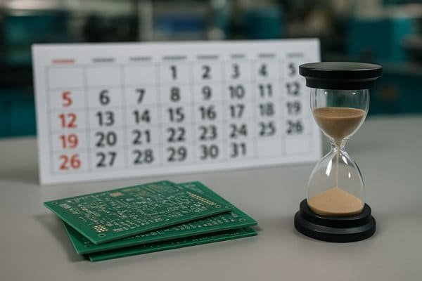
What is the Turnaround Time for PCB?
Need your boards fast? Fabrication delays can stall your prototyping. Understanding manufacturing turnaround is key to keeping your project moving.
Standard prototype PCB fabrication (2-4 layers, FR-4) is typically 3-7 working days. Expedited services can offer 24-72 hour turnarounds for simple boards. Complex boards (many layers, special materials, tight tolerances) can take 7-15 working days or more.
When I'm working on a tight deadline, like debugging the PACE evaluation board at Lightelligence, every day counts. The turnaround time for PCB fabrication directly impacts how quickly we can test iterations. Knowing what manufacturers can offer and what factors drive their timelines is critical. It's not just about how fast they can make a board, but also about the quality they can maintain at that speed. The time it takes to manufacture a bare PCB depends on several aspects. For some aerospace projects, we used specific high-reliability materials4 that added a week to the fab time. Always confirm lead times with your chosen manufacturer, especially for non-standard requirements.
| Factor | Typical Impact on Turnaround Time | Example |
|---|---|---|
| Layer Count | More layers = more processing steps (lamination, plating) | 2-layer: 1-5 days; 8+ layers: 5-10+ days |
| Material | Standard FR-4 is fastest; specialized materials (Rogers, High-Tg) longer | Rogers material: may add 2-5 days |
| Surface Finish | HASL is quick; ENIG, Immersion Silver may add 12-24 hours | ENIG: +0.5 to 1 day |
| Complexity/Tolerances | Fine lines (<4mil), microvias, blind/buried vias, impedance control | Blind/buried vias: can add 2-5 days |
| Quantity | Prototypes (1-50) faster than small/medium volume (50-1000+) | Production (1000+): 2-6 weeks |
| Manufacturer Workload | High capacity utilization or limited tech can increase lead times | Check with supplier; can vary seasonally or by fab capability |
How Long Does PCB Assembly Take?
Boards fabricated but not assembled? The assembly process has its own timeline. Knowing this helps you estimate when you'll have functional prototypes.
PCB assembly (PCBA) for prototypes (1-10 units) typically takes 3-7 working days if all components are kitted. For low to mid-volume production (50-1000 units), expect 1-3 weeks. Turnkey services including component sourcing can add 1-4 weeks for sourcing.
Once the bare PCBs arrive, the next critical step is assembly. I've seen projects get significantly delayed at this stage, especially if component sourcing wasn't planned well. At Honeywell, for the Tuxedo Keypad, managing the assembly timeline across multiple SKUs and global markets was a complex logistical challenge. Smooth assembly requires good preparation, clear documentation, and a reliable assembly partner. The duration of PCB assembly depends on several factors. During chip shortages, sourcing certain microcontrollers could add months. For typical prototype runs where components are kitted, many assembly houses offer 3-5 day turns.
| Assembly Stage | Typical Duration (Prototypes, Kitted) | Notes |
|---|---|---|
| Component Sourcing (Turnkey) | 1-12+ weeks | Biggest variable; hard-to-find parts cause major delays. |
| Kit Preparation/Verification | 1-2 days (if customer kitted) | Assembler verifies parts against BOM. |
| SMT Setup & Assembly | 1-2 days | Includes stencil prep, machine programming, placement, reflow. |
| THT Assembly | 0.5-1 day (if applicable) | Manual insertion or selective soldering. |
| Inspection (AOI, X-Ray) | 0.5-1 day | AOI is quick; X-ray for BGAs/QFNs takes longer. |
| Functional Test (FCT) | Varies (0.5 - 2+ days) | Highly dependent on test complexity and duration per board. |
| Rework (if needed) | Varies (hours to days) | Unplanned; depends on issues found. |
What is the Average Cost of a PCB?
Budgeting for your project? PCB costs can vary wildly. Understanding the contributing factors helps you estimate expenses more accurately.
A simple 2-layer prototype PCB (e.g., 100x100mm) might cost $5-$20 per piece for small quantities (1-10). A complex 8-layer board with controlled impedance could be $100-$500+ per piece in prototype quantities. Mass production significantly reduces per-unit costs.
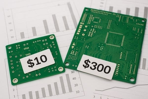
The "average cost" of a PCB is a bit like asking the average cost of a car – it depends immensely on the make, model, and features. I've worked on projects where prototype PCBs were a few dollars each, and others, especially in aerospace or with advanced technologies like photonic chips, where a single prototype board could cost thousands. It's all about the specifics of your design and manufacturing requirements. The price of a printed circuit board is influenced by numerous variables. When I managed cost-reduction projects at Honeywell, we often had to re-architect systems to use simpler, lower-layer-count PCBs. Always get quotes from multiple manufacturers.
| Cost Factor | Impact | Example (Relative to 2-Layer FR-4 100x100mm, 1oz Cu, HASL) |
|---|---|---|
| Size & Quantity | Larger = more material; Higher qty = lower per-unit cost | 10pcs: ~$5-15/pc; 1000pcs: ~$0.50-2/pc |
| Number of Layers | More layers = more material & processing | 4-layer: ~1.5-2x cost of 2-layer; 8-layer: ~3-5x cost of 2-layer |
| Material Type | FR-4 (standard) is cheapest; High-Tg, Rogers, Flex add cost | Rogers: 3-10x cost of FR-4; Flex: 3-10x cost of rigid FR-4 |
| Board/Copper Thickness | Thicker board/copper adds cost | 2oz copper: +10-20% vs 1oz |
| Min. Track/Space, Hole Size | Tighter tolerances (<4mil track/space, <0.2mm drill) increase cost | <4mil T/S: +10-50% |
| Surface Finish | HASL (cheapest); ENIG, Immersion Ag/Au add cost | ENIG: + ~$0.01-0.05/sq.inch |
| Special Requirements | Controlled impedance, blind/buried vias, via-in-pad add cost | Controlled Impedance: +10-20%; Blind/Buried Vias: +30-100%+ |
How Long Do PCBs Take to Ship?
Are your boards manufactured but stuck in transit? Shipping time is a crucial part of the overall lead time. Knowing your options can save you days or weeks.
Express international shipping (e.g., DHL, FedEx, UPS) from Asia to North America or Europe typically takes 3-7 working days. Standard air freight might take 7-14 days. Sea freight is much longer, 4-8 weeks, but is cost-effective for large volumes.

Once your PCBs are fabricated and assembled, getting them to your lab or production facility is the final hurdle. In my experience, especially with time-sensitive projects like the initial bring-up of the photonic computing chip evaluation board, opting for express shipping was non-negotiable, despite the higher cost. For high-volume products like the Tuxedo Keypad, we planned production schedules to accommodate more economical sea freight. The time it takes for PCBs to reach you depends heavily on the origin, destination, and chosen shipping method. Customs clearance can occasionally add a day or two, even with express couriers.
| Shipping Method | Typical Duration (International from Asia to NA/Europe) | Cost | Notes |
|---|---|---|---|
| Domestic (within same country) | 1-5 working days | Low-Med | Ground is cheaper, Express is faster. |
| International Express Courier | 3-7 working days | High | DHL, FedEx, UPS. Good for prototypes, small/medium volumes. |
| International Standard Air Freight | 7-14 days | Medium | Airport-to-airport, then local delivery. |
| International Sea Freight | 4-8+ weeks | Low | Port-to-port. Best for very large, non-urgent shipments. |
What is the Life Expectancy of a PCB?
Designing for longevity? The lifespan of a PCB is critical for product reliability. Knowing what influences it helps you build durable systems.
A well-designed and manufactured PCB, used within its specified operating conditions, can have a life expectancy of 10-20 years or more for industrial applications. Consumer electronics PCBs might be designed for 3-7 years. Harsh environments significantly reduce this.
The question of PCB lifespan is vital, especially in industries like aerospace, medical devices, or industrial automation where reliability is paramount. During my time at Smiths Medical developing infusion pumps, the expected operational life was a key design constraint. A PCB itself, if not subjected to extreme stress, is quite robust. The "life expectancy" is more often dictated by the components mounted on it or the environmental conditions. According to IPC-2221, the glass transition temperature (Tg)5 of standard FR-4 is typically 130-180°C; operating near or above Tg degrades the material. For critical applications, "Design for Reliability6" (DfR) principles are applied.
| Factor | Impact on Lifespan | Mitigation / Consideration |
|---|---|---|
| Component Reliability | Dominant factor; electrolytic caps, ICs have finite life (e.g., 2,000-10,000 hrs for some caps at max temp). | Select high-reliability parts, check MTBF/MTTF data. |
| Operating Temperature | High temps accelerate aging (Arrhenius law); thermal cycling causes fatigue. | Heatsinking, airflow, derating, higher Tg PCB material (e.g., >170°C). |
| Humidity/Contaminants | Can cause corrosion, electrical leakage, material degradation. | Conformal coating, enclosure design. |
| Vibration/Mech. Stress | Can cause solder joint fatigue, component detachment, PCB cracks. | Potting, ruggedized components, strain relief, proper mounting. |
| PCB Material Quality | Laminate, copper adhesion, solder mask quality affect long-term stability. | Use reputable suppliers, specify material grades (e.g., IPC-4101). |
| Manufacturing Quality | Poor soldering, contamination, delamination create latent defects. | IPC-A-600/610 compliance, process control. |
| Design Margins (Derating) | Operating components near max ratings reduces life. | Derate components (e.g., power, voltage, current) by 20-50%. |
What is the Failure Rate of PCB?
Concerned about field returns? Understanding PCB failure rates is key to building reliable products. Knowing common causes helps in prevention.
The intrinsic failure rate of a bare PCB (if well-manufactured) is very low, often less than 10-50 FIT (Failures In Time, i.e., failures per billion hours). Most "PCB failures" are actually component failures or assembly defects (e.g., solder joints).
When discussing PCB failure rates, it's important to distinguish between the bare board itself and the assembled board (PCBA). In my experience, a properly designed and fabricated bare PCB is rarely the root cause of failure. At Honeywell, we tracked field return data, and most issues pointed towards component wear-out or assembly weaknesses. A Class 2 board (IPC-A-6007) might have an outgoing defect rate of <0.1% from a good supplier. A complete PCBA for an industrial controller might aim for an MTBF8 of 200,000 to 1,000,000+ hours (1,000 to 5,000 FIT).
| Failure Source Category | Common Causes | Typical Failure Rate Impact | Prevention/Mitigation |
|---|---|---|---|
| Bare PCB Defects | Delamination, open/short traces (fab errors), material breakdown (long-term) | Very Low (<10-50 FIT for the board itself) | Quality fab (IPC-A-600), material selection. |
| Component Failures | End-of-life, electrical overstress (EOS), manufacturing defects in component | High (Dominant factor, sum of all component FIT rates) | Component selection, derating, supplier quality. |
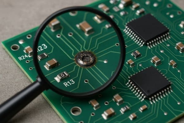
| Solder Joint Failures | Thermal cycling, vibration, poor initial soldering, intermetallic growth | Medium to High (depends on stress and initial quality) | IPC-A-610 compliance, process control, strain relief. |
| Contamination/Corrosion | Manufacturing residues, environmental exposure | Low to Medium (if unprotected in harsh environments) | Cleaning, conformal coating. |
| EOS/ESD | Electrical overstress, electrostatic discharge during handling/operation | Low to Medium (depends on protection measures) | ESD protection design, proper handling procedures. |
How Many Times Can You Rework a PCB?
Need to modify or repair a board? Rework is common, but has its limits. Knowing how many times is safe preserves board integrity.
Most PCBs can tolerate 2-4 localized rework cycles (e.g., removing and replacing a component) without significant degradation. However, IPC-7711/7721 guidelines suggest minimizing rework. Excessive heat or mechanical stress during rework can damage pads, traces, or delaminate the board.
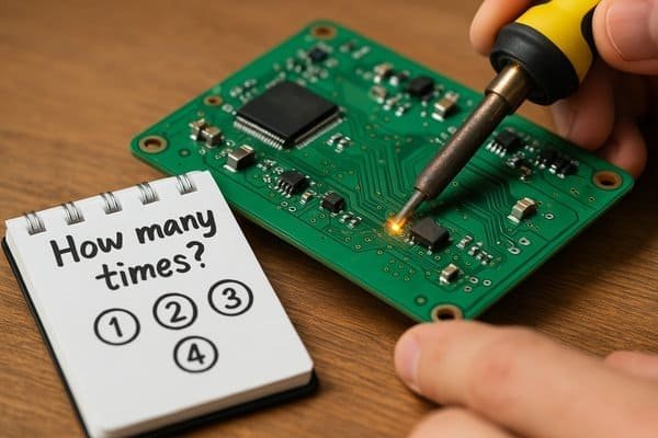
Rework is an inevitable part of hardware development. I've spent countless hours reworking prototypes. The key is to do it carefully and understand that each rework cycle thermally and mechanically stresses the board. For the photonic chip evaluation board, we performed highly delicate rework; each attempt was meticulous. The ability of a PCB to withstand rework depends on several factors. IPC guidelines (IPC-7711/7721)9 recommend minimizing rework operations on the same location. For Class 3 products (high-reliability), rework is often much more restricted. If a location needs more than 2-3 rework attempts, consider scrapping the board.
| Factor Influencing Rework Tolerance | Details | Rework Limit Guideline (General) |
|---|---|---|
| PCB Quality & Material10 | Higher Tg, good copper adhesion withstand more heat. Cheaper boards damage easily. | Higher quality = more tolerance |
| Component Type | THT easier than SMT. BGAs are most sensitive. | THT: 3-5 cycles; SMD: 2-4 cycles; BGA: 1-2 cycles (specialized equip.) |
| Rework Skill & Equipment11 | Skilled tech with proper tools (temp control, hot air, preheaters) is crucial. | Proper technique extends limits |
| Pad & Trace Size | Small, delicate pads/traces lift or damage more easily. | Robust features = more tolerance |
| Heat Applied | Excessive heat/duration is the primary cause of delamination and pad lift. | Minimize heat exposure |
Conclusion
Understanding PCB lead times, costs, and reliability factors is key. This knowledge helps you plan projects effectively, manage budgets, and build dependable hardware.
-
Learning about the importance of a designer's experience can guide you in selecting the right partner for your project. ↩
-
Understanding the impact of design complexity on costs can help you budget more effectively for your project. ↩
-
Exploring signal integrity requirements is crucial for ensuring high-performance PCB designs. ↩
-
Exploring this topic can provide insights into material choices that enhance PCB performance and reliability. ↩
-
Exploring Tg's impact on PCB materials helps in selecting the right components for longevity and performance. ↩
-
Understanding DfR principles can significantly enhance the reliability and lifespan of PCBs in critical applications. ↩
-
The IPC-A-600 standard is vital for ensuring PCB quality; learning about it can improve your design and manufacturing processes. ↩
-
MTBF is a key metric for reliability in electronics; exploring this can enhance your knowledge of product longevity. ↩
-
Understanding IPC guidelines is crucial for ensuring high-quality PCB rework and reliability in hardware development. ↩
-
Exploring the impact of PCB quality on rework tolerance can help you choose the right materials for your projects. ↩
-
Learning about the essential skills and equipment for PCB rework can enhance your rework processes and outcomes. ↩


