EMI issues can cripple your RF PCB performance, causing endless frustration. Effective EMI reduction methods, thoughtfully applied, are crucial for a successful and clean RF design.
Key EMI reduction methods in RF PCB design include a solid ground plane, proper component placement and circuit partitioning, RF shielding, careful trace routing with controlled impedance, appropriate use of bypass capacitors and ferrite beads, and techniques like via stitching and guard traces.

Understanding and implementing these methods is essential for any hardware engineer working with radio frequencies. Without them, your brilliant RF design might get lost in a sea of noise, leading to poor performance, failed compliance tests, and endless debugging. I've seen many projects struggle because these fundamental aspects were overlooked. Let's dive into specific techniques that can help you keep EMI under control and ensure your RF circuits perform as intended.
What are typical EMI sources affecting RF PCBs?
Is your RF circuit underperforming due to mysterious noise interference? Identifying these EMI culprits is the critical first step towards achieving a clean and robust RF design.
Typical EMI sources affecting RF PCBs include high-frequency digital logic, switching power supplies, oscillators, power amplifiers, antennas (self-interference), and external radiators like mobile phones or Wi-Fi routers. These can couple noise through conduction or radiation.
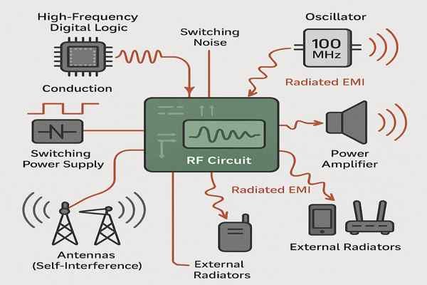
Understanding Common EMI Sources in RF Designs
In my experience, EMI issues in RF PCBs often stem from a mix of on-board and off-board culprits. Understanding these sources is key to devising effective mitigation strategies.
Internal EMI Sources
These originate from components and signals on the PCB itself. They are often the primary focus of on-board EMI control.
- Digital Circuits: Microcontrollers (\(\text{MCUs}\)), FPGAs, and high-speed data buses are notorious. Their fast-switching clock signals and data lines generate a broad spectrum of harmonics. For instance, a \(100 \text{ MHz}\) clock doesn't just create noise at \(100 \text{ MHz}\); its harmonics at \(200 \text{ MHz}\), \(300 \text{ MHz}\), and so on, can extend well into sensitive RF bands.
- Switching Mode Power Supplies (\(\text{SMPS}\))1: These are efficient but can be very noisy. The rapid switching of transistors and diodes (often from tens of \(\text{kHz}\) to several \(\text{MHz}\)) generates broadband noise that can conduct through power lines or radiate.
- RF Components: Oscillators (like Voltage-Controlled Oscillators, \(\text{VCOs}\), or Crystal Oscillators, \(\text{XOs}\)), Mixers, and Power Amplifiers (\(\text{PAs}\)) are fundamental to RF circuits but can also be sources of unwanted signals, like harmonics and intermodulation products.
External EMI Sources
These come from the environment surrounding the PCB and can be coupled into your circuit.
- Other Electronic Devices: Nearby mobile phones, Wi-Fi routers, other transmitters, or even industrial machinery can radiate fields that interfere with your RF PCB.
- Environmental Factors: Electrostatic Discharge (\(\text{ESD}\))2 events, power line transients, and emissions from motors or fluorescent lighting can also inject disruptive energy.
Coupling Mechanisms
Noise needs a way to travel from the source to the victim circuit. Understanding these paths is crucial.
- Conducted EMI: Noise travels along PCB traces, power and ground planes, and cables.
- Radiated EMI: Noise travels through the air as electromagnetic waves, either from a source to your PCB or from your PCB to other devices.
Here's a summary table:
| Category | Source Type | Examples | Primary Coupling |
|---|---|---|---|
| Internal EMI | Digital Circuits | MCUs, FPGAs, high-speed data buses, clock signals | Radiated, Conducted |
| Power Supplies | SMPS | Radiated, Conducted | |
| RF Components | Oscillators, Mixers, PAs | Radiated, Conducted | |
| External EMI | Electronic Devices | Mobile phones, Wi-Fi routers, nearby transmitters | Radiated |
| Environmental | ESD, power line transients, motors | Radiated, Conducted |
Relevant Standards
International standards like CISPR 223 (or its European equivalent EN 55022) set limits for unintentional emissions from Information Technology Equipment, which often includes devices with RF PCBs. Meeting these standards requires a proactive approach to EMI control from the start of the design.
How does a solid ground plane on an RF PCB reduce EMI?
Are unstable ground references creating a noisy nightmare for your RF signals? A robust ground plane isn't just a good idea; it's foundational for EMI reduction.
A solid ground plane on an RF PCB significantly reduces EMI by providing a low-impedance return path for high-frequency currents, minimizing problematic ground loop areas, and offering a degree of shielding for signal traces.
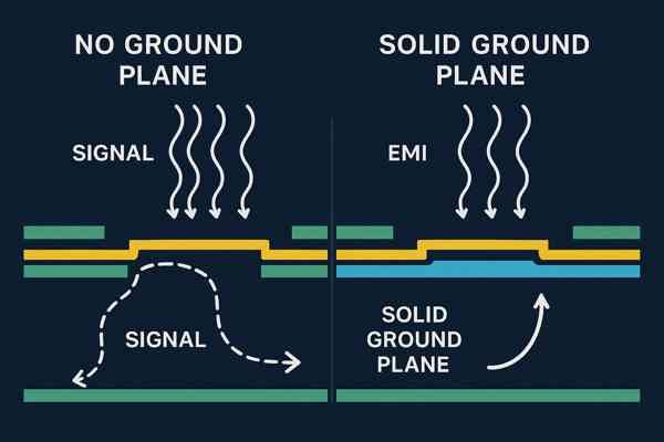
The Crucial Role of a Solid Ground Plane in EMI Mitigation
I can't stress enough the importance of a good ground plane4, especially in RF design. It's often the most critical factor for EMI control. A well-designed ground plane offers multiple benefits compared to poorly designed or segmented grounding schemes.
Low-Impedance Return Path Explained
High-frequency signals need a direct, low-impedance path back to their source. A continuous ground plane directly under (or over) a signal trace provides this. This minimizes the loop area formed by the signal and its return current, which in turn reduces radiated emissions (\(E_{field} \propto Area \cdot I \cdot f^2\)) and susceptibility. According to IPC-2221 (Generic Standard on Printed Board Design), Section 5.3.2, "The use of ground planes is the preferred method for providing the lowest impedance ground system." A lower impedance means less voltage drop across the ground structure, reducing common-mode noise.
Impact on Ground Loops and Shielding
Ground loops occur when multiple paths exist for ground currents, creating potential differences between various ground points. These loops can act as antennas. A solid ground plane helps ensure all ground references are as close to the same potential as possible, effectively eliminating most ground loop problems within the PCB. While not a perfect shield, a ground plane does offer some shielding by containing electric fields between the signal traces and the plane. It can also help absorb or reflect some incident radiated energy.
Importance for Signal Integrity and Vias
A stable and continuous ground reference is crucial for maintaining controlled impedance for transmission lines (like microstrips or striplines). Impedance discontinuities are a source of reflections and EMI. Furthermore, vias connecting components or traces to the ground plane will have lower parasitic inductance if they connect directly to a large, solid plane rather than a routed ground trace. I always try to use multiple vias for ground connections of critical components to further reduce this inductance.
Here's a comparison:
| Feature | Benefit of Solid Ground Plane | Consequence of Poor/Split Ground Plane |
|---|---|---|
| Return Path Impedance | Provides a very low impedance path for RF currents. | High impedance, leading to common-mode noise. |
| Ground Loops | Minimizes or eliminates ground loop areas. | Creates potential for large, problematic ground loops5. |
| Shielding | Offers inherent shielding for traces against radiated noise. | Reduced or ineffective shielding. |
| Signal Integrity | Ensures a stable reference for controlled impedance traces. | Impedance discontinuities, reflections, and signal issues. |
| Via Inductance | Lowers inductance for vias connecting to ground. | Higher via inductance. |
| Current Loop Area | Keeps signal and return current paths close, minimizing loop area. | Can force large return current loops, increasing EMI. |
It's generally bad practice to have splits or large cutouts in the ground plane under critical RF traces. If a signal has to cross such a discontinuity, its return current is forced to take a detour, creating a large loop and, consequently, EMI.
What is the main benefit of using RF shielding cans?
Are your sensitive RF components swamped by noise, or are noisy parts radiating excessively? RF shielding cans provide a robust, localized solution to contain and protect.
The main benefit of using RF shielding cans is to isolate sensitive RF circuits from external electromagnetic interference (EMI) and to contain emissions from potentially noisy components, effectively creating a small Faraday cage on the PCB.
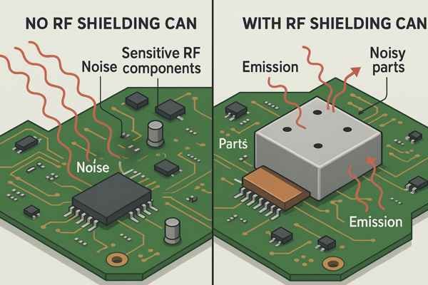
Maximizing Isolation with RF Shielding Cans
In many of my RF designs, especially those with high sensitivity or high power, RF shielding cans6 are indispensable. They act like little metal fortresses for specific circuit sections.
The Faraday Cage Principle in Action
An RF shield works on the principle of a Faraday cage7. It's a conductive enclosure that blocks external static and non-static electromagnetic fields and contains internally generated fields. The effectiveness depends on the material, its thickness, the frequency of the EMI, and the integrity of the shield (no large gaps).
Material and Shielding Effectiveness8 (\(SE\))
Common materials include tin-plated steel, brass, or nickel silver. The Shielding Effectiveness (\(SE\)) is a measure of how much the shield attenuates EMI, usually expressed in decibels (\(\text{dB}\)). For instance, a typical \(0.2 \text{ mm}\) thick steel can might offer \(>40 \text{ dB } SE\) up to several gigahertz (\(\text{GHz}\)). The actual \(SE\) is influenced by factors like material permeability, conductivity, and thickness, as well as the frequency of the interference. For very high frequencies, even small apertures can compromise shielding.
Critical Design and Mounting Considerations
When implementing shielding cans, several factors are crucial for their performance:
| Consideration | Description | Importance |
|---|---|---|
| Material | Tin-plated steel, brass, nickel silver. Thickness affects \(SE\). E.g., \(0.2 \text{ mm}\) steel can offer \(>40 \text{ dB } SE\) up to several \(\text{GHz}\). | Crucial for attenuation level and frequency range. |
| Grounding | Must be well-grounded to PCB ground plane at multiple points via solder tabs or spring fingers. | Essential for shield to function; poor grounding can make it an antenna. |
| Apertures/Holes | For ventilation or I/O. Maximum dimension should be \(\ll \lambda\) (wavelength of highest concern frequency), e.g., \(< \lambda/10\) or even \(< \lambda/20\). | Large or unmanaged openings compromise shielding integrity. |
| Construction Type | One-piece (soldered) or two-piece (frame with removable lid). | Two-piece allows access for rework/prototyping. |
| I/O Filtering | Signals passing through shield walls may need feed-through capacitors or filters. | Maintains shield integrity for signals entering/leaving the enclosure. |
I typically use shielding cans for VCOs, Low Noise Amplifiers (\(\text{LNAs}\)), Power Amplifiers (\(\text{PAs}\)), and other sensitive or noisy RF stages. While they add cost and complexity, their benefit in critical applications is undeniable.
How does circuit partitioning on a PCB help control EMI?
Do different circuit types on your PCB seem to be in a constant battle, creating interference? Smart circuit partitioning is like establishing peaceful, well-defined neighborhoods for harmonious operation.
Circuit partitioning on a PCB helps control EMI by physically separating noisy circuit blocks (like digital logic or power supplies) from sensitive circuit blocks (like RF amplifiers or analog inputs). This minimizes undesirable cross-coupling of noise between them.
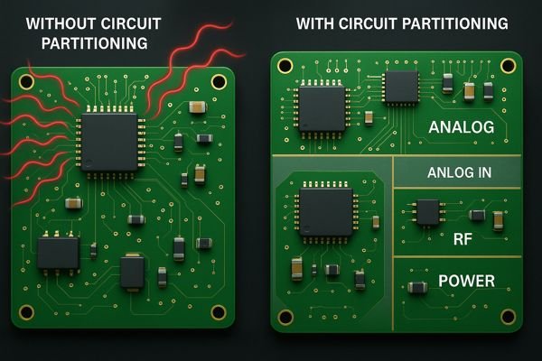
Strategic Circuit Partitioning for EMI Control
I always think of circuit partitioning as drawing clear boundaries. It's a fundamental layout strategy for any mixed-signal or RF board.
Defining "Quiet" and "Noisy" Zones
The core idea is to identify which parts of your circuit are likely to generate EMI ("noisy") and which parts are susceptible to EMI ("quiet" or "sensitive"). Then, you physically separate these zones on the PCB layout.
| Zone Type | Circuit Examples | Key Strategy |
|---|---|---|
| Noisy Zones | Digital logic (MCUs, FPGAs), High-speed buses, SMPS | Group together, keep away from sensitive areas, control routing of their signals/power. |
| Sensitive Zones | RF front-ends (LNAs), Analog inputs, VCOs, PLLs | Group together, protect from noisy zones, ensure clean power and ground references. |
| Interface Zones | ADCs, DACs, mixed-signal ICs | Careful placement at the boundary, meticulous grounding and power supply filtering. |
Practical Implementation Techniques
Effective partitioning involves several layout strategies:
- Physical Separation: Maximize the distance between noisy and sensitive sections. This is the simplest form of partitioning.
- Grounding Strategy: Preferably use a continuous ground plane, with digital circuits and their return currents confined to one area of the plane, and analog/RF circuits to another. If split grounds are used (less common for high-frequency RF), manage the split and any signal crossings with extreme care. Henry Ott in his book "Electromagnetic Compatibility Engineering" provides extensive guidance on how to do this correctly, typically with a star point connection or a bridge, but emphasizes the risks if done poorly.
- Power Distribution: Use separate, filtered power supply rails for different partitions. For example, an LDO might feed a sensitive RF section, itself powered from a slightly noisier SMPS output that supplies digital sections.
- Signal Routing: Avoid routing noisy digital traces near or parallel to sensitive analog/RF traces. If they must cross, try to do so at a \(90^\circ\) angle to minimize capacitive coupling.
Benefits of Effective Partitioning
By thoughtfully partitioning your PCB, you can significantly reduce common impedance coupling9 (noise shared through common ground or power paths) and radiated coupling between functional blocks, leading to a much more stable and EMI-resilient design.
Where should bypass capacitors be placed for best EMI filtering?
Are noisy power rails compromising your RF signals and causing ICs to misbehave? The precise placement of bypass capacitors is a micro-detail with a macro-level impact on EMI.
For best EMI filtering, bypass capacitors should be placed as close as physically possible to the power and ground pins of the IC they are decoupling. The smallest value capacitor (for highest frequencies) should be the absolute closest.
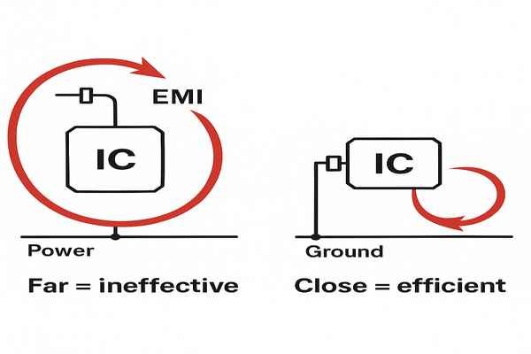
Optimizing Bypass Capacitor Placement for Effective Filtering
I've spent countless hours debugging issues that ultimately traced back to suboptimal bypass capacitor placement or selection.
The Purpose of Bypass Capacitors
Integrated circuits (\(\text{ICs}\)) draw current in fast bursts, especially digital ICs and RF components. Bypass (or decoupling) capacitors act as local, low-inductance charge reservoirs, supplying this instantaneous current. This prevents the IC from creating noise on the power distribution network (\(\text{PDN}\)) and ensures the IC itself receives stable power.
Why Proximity is Paramount
The goal is to minimize the inductance in the path from the capacitor through the IC's power/ground pins and back to the ground plane. Every millimeter of PCB trace adds inductance, typically in the range of \(0.5 \text{ nH/mm}\) to \(1 \text{ nH/mm}\). At high frequencies, even a few nanohenries (\(\text{nH}\)) can significantly impede the capacitor's ability to supply current quickly. "As close as possible" means just that – often on the same side of the PCB as the IC, right next to the pins. Vias connecting the capacitor to the power and ground planes also add inductance and should be short, wide (if possible), and placed very close to the capacitor pads.
Strategies for Multiple Capacitor Values
It's standard practice to use a parallel combination of capacitors with different values at each IC or group of ICs to cover different frequency ranges. The capacitor with the lowest value (and thus typically the best high-frequency response) should always be the one physically closest to the IC pins.
A common scheme might be:
- \(10 \text{ nF}\) (or \(100 \text{ nF}\)) ceramic for mid-to-high frequencies.
- Smaller ceramics like \(100 \text{ pF}\) or \(1 \text{ nF}\) for very high RF frequencies.
- Larger tantalum or electrolytic capacitors (e.g., \(1 \mu\text{F}\) to \(100 \mu\text{F}\)) placed nearby (within a cm or two) for lower frequency bypassing and bulk charge.
Understanding Capacitor Characteristics (\(ESL\)/\(ESR\))
For high-frequency bypassing, choose capacitors with low Equivalent Series Inductance10 (\(ESL\)) and low Equivalent Series Resistance (\(ESR\)). Surface-mount ceramic capacitors (\(\text{SMDs}\)) are generally good for this.
Key rules summary:
| Rule | Guideline | Rationale |
|---|---|---|
| Proximity to IC Pins | Place capacitor pads immediately adjacent to IC power and ground pins. | Minimizes trace inductance (approx. \(0.5-1 \text{ nH/mm}\)); every mm counts at high frequencies. |
| Smallest Value Closest | If using multiple bypass capacitors11 of different values, the one with the smallest capacitance (e.g., \(100 \text{ pF}\), \(1 \text{ nF}\) for RF) goes closest. | Smallest capacitors have the best high-frequency response and lowest \(ESL\) for tackling fast transients. |
| Via Placement | Vias connecting capacitor to power/ground planes should be very close to capacitor pads, and preferably use multiple vias for low inductance. | Via inductance adds to the total loop inductance. |
| Multiple Values | Use a range of values (e.g., \(100 \text{ pF}\), \(10 \text{ nF}\), \(1 \mu\text{F}\), \(10 \mu\text{F}\)) in parallel. | Addresses different frequency components of noise. |
| Capacitor Type | Choose low \(ESL\) and low \(ESR\) ceramic capacitors (\(\text{SMDs}\)) for high frequencies. | Ensures capacitor behaves like a capacitor, not an inductor, at target frequencies. |
Many IC manufacturers, like Analog Devices (see AN-1349), provide specific decoupling recommendations.
What is the function of a ferrite bead on an RF PCB power line?
Is high-frequency noise from digital circuits or SMPS traveling along your power lines and disrupting sensitive RF stages? A ferrite bead can act as a selective filter.
A ferrite bead on an RF PCB power line functions as a high-frequency filter, presenting a high impedance to unwanted RF noise signals while allowing DC current to pass with minimal opposition. It essentially dissipates the noise energy as heat.
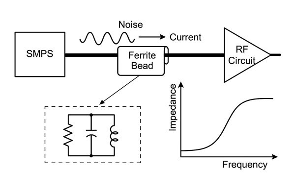
Utilizing Ferrite Beads for Power Line Noise Suppression
I often use ferrite beads12 as a simple yet effective way to clean up power supply lines, especially when isolating different sections of an RF board.
How Ferrite Beads Function
A ferrite bead is a passive electronic component. At low frequencies (like DC or low-frequency AC), it acts like a small inductor with very low impedance. However, as frequency increases into the RF range (typically \(\text{MHz}\) to \(\text{GHz}\)), the ferrite material exhibits properties that cause the bead's impedance to become primarily resistive. This high, frequency-dependent impedance effectively blocks or attenuates high-frequency noise. The resistive component means the absorbed RF energy is converted into a small amount of heat.
Interpreting Impedance Characteristics (\(Z, R, X_{L}\))
Ferrite beads are characterized by their impedance (\(Z\)) versus frequency curve. This impedance has both resistive (\(R\)) and reactive (\(X_{L}\)) components: \(Z = R + jX_{L}\). Manufacturers provide plots showing these values. For noise filtering, you typically want a bead that has a high resistive component (\(R\)) at the noise frequencies you're trying to suppress.
Key Selection Criteria for Ferrite Beads
Choosing the right ferrite bead involves several considerations:
| Parameter | Consideration | Impact on Performance |
|---|---|---|
| Impedance (\(Z\)) @ Freq | Choose a bead with high impedance (e.g., \(50 \Omega\) to \(>1 \text{ k}\Omega\)) at the target noise frequencies (e.g., \(100 \text{ MHz}\)). Check \(Z\), \(R\), and \(X_{L}\) curves. | Higher impedance (especially resistive component \(R\)) provides better attenuation. |
| DC Bias Current (\(I_{DC}\)) | Select a bead whose impedance characteristics13 are maintained at the operating DC current. | Exceeding rated \(I_{DC}\) can saturate the ferrite, drastically reducing its impedance. |
| Frequency Range | Ensure the bead is effective across the entire spectrum of noise you need to suppress. | Different ferrite materials have different optimal frequency ranges. |
| Size/Package | Choose an appropriate SMD size for your layout and current handling needs. | Physical constraints and power dissipation. |
Effective Placement and Combined Usage
Ferrite beads are placed in series with the power line, usually close to the component or circuit section you want to protect or isolate. They are often used in conjunction with bypass capacitors to form a Pi-filter (Capacitor-Bead-Capacitor) or L-filter (Bead-Capacitor or Capacitor-Bead) for enhanced filtering performance. Companies like Murata and Würth Elektronik (their "Trilogy of Magnetics" is an excellent resource) offer extensive data and application notes.
What RF trace routing tips help lower EMI?
Are your RF traces behaving like unintentional antennas, radiating energy or becoming overly susceptible to noise? Proper RF trace routing is not just about connectivity; it's about signal integrity.
Key RF trace routing tips to lower EMI include maintaining controlled impedance (typically \(50 \Omega\)), keeping traces as short as possible, using gentle bends (\(45^\circ\) or curved, not sharp \(90^\circ\)), ensuring adequate spacing from other traces (especially digital or noisy ones), and routing over a continuous ground plane.
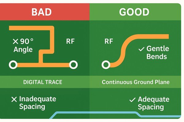
Best Practices for RF Trace Routing to Minimize EMI
Routing RF traces is about creating well-behaved transmission lines. I always adhere to these crucial guidelines:
Achieving Controlled Impedance14 (e.g., \(50 \Omega\))
For most RF applications, traces are designed to have a characteristic impedance, commonly \(50 \Omega\). This requires careful calculation of trace width, dielectric material properties (like dielectric constant, \(D_{k}\) or \(\epsilon_{r}\)), and height above the ground plane for microstrip traces, or between ground planes for stripline traces. EDA tools have calculators for this. Impedance mismatches cause reflections, signal loss, and potential EMI.
Geometric Considerations: Length, Bends, and Stubs
- Keep Traces Short: Shorter traces have less inductance and capacitance, radiate less, are less susceptible to picking up noise, and incur lower signal loss (\(IL\)), especially at higher RF frequencies.
- Gentle Bends: Sharp \(90^\circ\) bends in an RF trace can cause impedance discontinuities and reflections. It's much better to use \(45^\circ\) bends or, ideally, curved (arced) bends.
- Avoid Stubs15: Unintended stubs (short, unterminated trace segments branching off the main signal path) can act as resonant elements, causing dips or peaks in the frequency response and potential EMI issues.
Spacing and Layer Management for Crosstalk Reduction
- Trace Spacing: Maintain sufficient spacing between parallel RF traces to minimize crosstalk. Keep RF traces far away from high-speed digital lines, clock signals, and switching power supply noise. The "3W rule" (space between traces is at least three times the trace width, center to center) is a common guideline for general digital design, but for RF, I often need more generous spacing or use guard traces.
- Route Over Solid Ground: Ensure RF traces always have a continuous, uninterrupted ground plane directly beneath (or above) them. This provides a clear, low-inductance return path.
- Avoid Parallel Digital Runs: Minimize long parallel runs with high-speed digital signals. If crossing is necessary, try to do so at \(90^\circ\) to minimize capacitive coupling.
- Differential Pairs: If using differential RF signals, route them tightly coupled and length-matched.
Summary Table:
| Routing Tip | Guideline | Rationale for EMI Reduction |
|---|---|---|
| Controlled Impedance | Design traces for \(50 \Omega\) (common standard) using correct width, dielectric (\(D_{k}\)), and ground reference. | Prevents reflections, maximizes power transfer, reduces signal distortion and emissions. |
| Keep Traces Short | Minimize the physical length of all RF traces. | Reduces radiation/pickup (antenna effect), minimizes loss (\(IL\)) and delay. |
| Gentle Bends | Use \(45^\circ\) miters or, preferably, smooth curved bends. Avoid \(90^\circ\) sharp corners. | Minimizes impedance discontinuities and reflections at bends. |
| Trace Spacing | Maintain sufficient clearance from other signal traces, especially noisy digital lines or clocks (e.g., >3W rule as a start, more for RF). | Reduces crosstalk (capacitive and inductive coupling). |
| Route Over Solid Ground | Ensure RF traces always have a continuous, uninterrupted ground plane directly beneath (or above) them. | Provides a low-inductance return path, minimizes loop area. |
| Avoid Parallel Digital Runs | Minimize long parallel runs with high-speed digital signals. Cross at \(90^\circ\) if unavoidable. | Reduces crosstalk. |
| No Stubs | Eliminate or minimize any unterminated trace branches (stubs). | Stubs cause reflections and can act as resonant antennas. |
Many principles from texts like "High-Speed Digital Design: A Handbook of Black Magic" by Howard Johnson and Martin Graham, are relevant.
How does via stitching aid RF PCB EMI performance?
Does your ground plane feel less than solid, especially at edges or between isolated sections, potentially allowing RF energy leakage? Via stitching is a technique to reinforce your ground integrity.
Via stitching aids RF PCB EMI performance by connecting ground areas on different layers more thoroughly using multiple vias. This lowers ground impedance, minimizes unwanted resonant loop areas, and improves the shielding effectiveness of the ground plane, especially at PCB edges and between isolated sections.
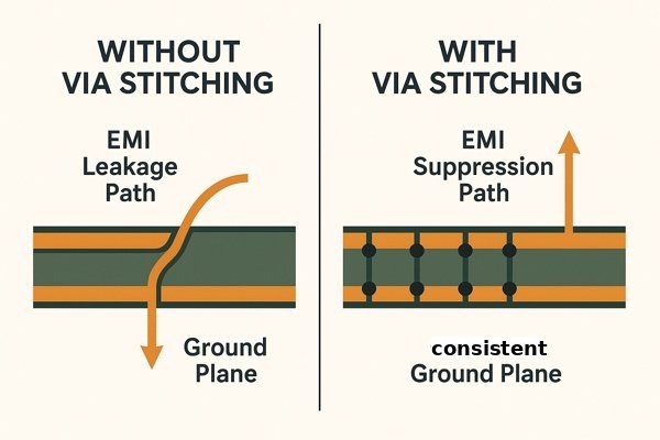
Enhancing Ground Integrity and Shielding with Via Stitching
Via stitching is a technique I frequently use to create a more robust ground environment, which is especially crucial at RF frequencies.
The Fundamental Purpose of Via Stitching
The main goal is to ensure that ground areas on different layers of the PCB (e.g., top ground pours and the main internal ground plane) are well-connected and behave as a single, unified low-impedance structure. It also helps to "contain" electromagnetic fields within desired regions and prevent leakage.
Practical Guidelines for Via Placement and Spacing
Via stitching involves placing an array or "fence" of vias that connect these ground areas.
- Placement Areas: Along PCB edges, around critical RF sections or traces, and within large ground pours to break up potential resonant modes.
- Spacing: A common rule of thumb for via stitching16 spacing is to place them at intervals of \(\lambda/10\) to \(\lambda/20\) or less, where \(\lambda\) is the wavelength of the highest frequency of concern in the PCB dielectric (e.g., FR-4 with \(\epsilon_{r} \approx 4.3\)). For a signal at \(5 \text{ GHz}\), \(\lambda\) in FR-4 is roughly \(2.9 \text{ cm}\). So, via spacing might be in the range of \(1.4 \text{ mm}\) to \(2.9 \text{ mm}\) or even closer for critical applications. The idea is that the spacing should be small enough so that the structure doesn't allow significant radiation or field leakage at the frequencies of interest.
| Via Stitching Aspect | Guideline / Purpose | Impact on EMI Performance |
|---|---|---|
| Placement Areas | Along PCB edges, around critical RF sections/traces, within large ground pours. | Contains fields, prevents edge radiation, isolates sections, suppresses resonances. |
| Via Spacing | Typically \(\lambda/10\) to \(\lambda/20\) of highest concern frequency (e.g., \(1.5 \text{ mm}\) to \(3 \text{ mm}\) for \(5 \text{ GHz}\)). | Prevents leakage/radiation between vias, ensuring the "fence" is effective. |
| Purpose | Ensure ground planes act as a single, low-impedance structure; improve isolation; reduce radiation from PCB edges. | Better ground integrity, improved shielding, reduced emissions. |
Advanced Technique: Micro-Coaxialization with Via Fences
For even greater RF isolation, particularly for critical traces, I've found that a more sophisticated approach involving meticulously designed via fences and ground guard bands can be highly effective. This technique aims to create localized "micro-coaxial" structures directly on the PCB. By flanking a critical RF trace with dense rows of stitching vias (the "via fence") on both sides—all connected to the main ground plane—and potentially adding ground guard traces parallel to the RF trace (also well-stitched), you essentially mimic the shielding of a coaxial cable. The RF trace becomes the "center conductor," and the surrounding grounded structures act as the "outer shield." This method can significantly enhance isolation, sometimes providing \(>10 \text{ dB}\) to \(20 \text{ dB}\) improvement in crosstalk reduction compared to unshielded traces, depending on the specific geometry and frequency. This transforms a simple planar transmission line into a more robustly shielded path.
Can PCB guard traces reduce noise coupling to RF lines?
Is crosstalk from noisy digital signals a persistent headache for your sensitive RF lines, even with some physical separation? PCB guard traces can act as localized shields.
Yes, PCB guard traces, when correctly implemented by grounding them at frequent intervals, can effectively reduce capacitive (electric field) noise coupling, or crosstalk, between an aggressor trace and a victim RF line by intercepting the interfering fields.
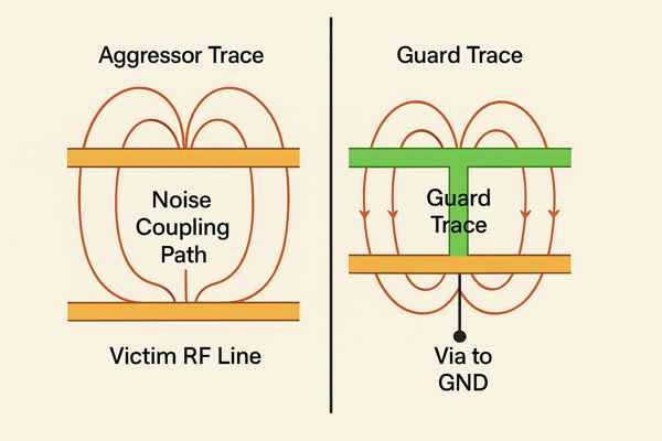
Employing Guard Traces17 to Mitigate Noise Coupling
Guard traces are a common technique I use to provide additional isolation for critical signals when physical separation alone isn't sufficient.
Mechanism of Guard Traces
A guard trace is typically a PCB trace connected to a stable reference voltage (usually ground) that is routed parallel to and between a potential noise source (aggressor trace) and a sensitive signal (victim trace). It intercepts the electric field lines that would otherwise couple from the aggressor to the victim, shunting the coupled noise current to ground.
Essential Implementation Rules for Effectiveness
For guard traces to be effective, they must be implemented correctly:
- Effective Grounding: This is the most crucial aspect. The guard trace must be solidly connected to the main ground plane at regular intervals using vias. If it's not well-grounded, the guard trace itself can float, pick up noise, and potentially re-radiate it, making the problem worse. The grounding interval should ideally be much shorter than the wavelength of the highest frequency of concern, similar to via stitching rules (e.g., every \(\lambda/20\) or less). For a \(2.4 \text{ GHz}\) signal, \(\lambda\) in FR-4 is about \(6 \text{ cm}\), so grounding vias every \(3 \text{ mm}\) or less would be good practice.
- Placement: The guard trace should be placed closer to the signal trace it is protecting than the aggressor trace is. It can be on one or both sides of the victim trace.
- Continuity: Ensure the entire length of the guard trace is properly grounded and continuous along the protected segment.
Expected Crosstalk Reduction18
A well-implemented guard trace can provide a significant reduction in crosstalk. The amount of reduction depends on the geometry (trace widths, spacing, dielectric height), frequency, and how well the guard trace is grounded. Reductions of \(6 \text{ dB}\) to over \(20 \text{ dB}\) are often cited in literature like Clayton R. Paul's "Introduction to Electromagnetic Compatibility," depending on the specifics.
| Guideline | Description | Rationale |
|---|---|---|
| Effective Grounding | Connect guard trace to main ground plane with vias at frequent intervals (e.g., every \(\lambda/20\) or less). | Prevents guard trace from floating, becoming an antenna, or re-radiating noise. This is critical. |
| Placement | Position between aggressor and victim trace, ideally closer to victim trace. Can be on one or both sides. | Intercepts electric field lines from aggressor before they reach victim. |
| Continuity | Ensure guard trace is continuous along the length of the protected signal trace segment. | Provides a consistent barrier. |
| Spacing | Optimize spacing between victim-guard and guard-aggressor based on trace widths and dielectric height. | Affects the efficiency of coupling interception. |
Guard traces are not a universal cure-all, and they consume PCB space. However, in targeted situations, they are a very useful tool.
What is a key grounding rule for mixed-signal (RF/Digital) PCBs?
Is digital noise from your microcontroller or processor corrupting sensitive RF and analog signals, making you question your entire grounding scheme? A unified but carefully planned strategy is vital.
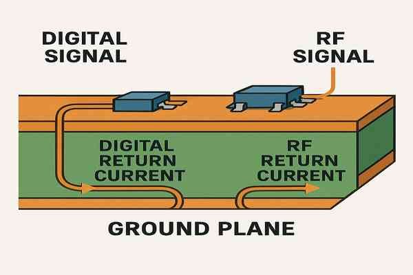
A key grounding rule for mixed-signal (RF/Digital) PCBs is to, whenever possible, use a solid, continuous ground plane for all circuits. Then, achieve isolation by carefully partitioning component placement and trace routing so that noisy digital return currents do not flow under or near sensitive RF/analog sections.
Mastering Grounding Strategies for Mixed-Signal RF PCBs
Grounding is often a point of confusion in mixed-signal PCB design. My experience, aligning with modern best practices for high-frequency designs, favors a unified ground plane managed by strategic layout.
The Unified vs. Split Ground Plane Dilemma
The debate between using a single, unified ground plane or splitting it into analog (\(\text{AGND}\)) and digital (\(\text{DGND}\)) sections has been ongoing for years.
| Grounding Approach | Description | Pros | Cons |
|---|---|---|---|
| Unified/Solid Ground Plane (with Partitioning) | Single continuous ground plane under all components. Isolation via physical separation of digital and analog/RF sections. | Lowest overall ground impedance. Clear return paths if layout is careful. Good for high frequencies. | Requires disciplined layout to prevent digital return currents from flowing under sensitive areas. |
| Split Ground Planes (\(\text{AGND}\)/\(\text{DGND}\)) | Separate analog and digital ground planes, connected at a single point (star ground). | Can prevent low-frequency digital noise from directly entering analog ground if done perfectly. | Difficult to manage at high frequencies. Risk of creating slot antennas. Signals crossing split cause large EMI loops. Prone to errors. |
Controlling Return Current Paths: The Key to Isolation
The modern preference, especially for designs involving RF and high-speed digital signals, is generally the unified ground plane approach with careful partitioning. High-frequency currents want to return directly underneath their signal traces. By grouping digital components and their traces in one distinct area of the board (over the unified ground plane) and analog/RF components and traces in their "analog/RF" area, their respective return currents will naturally stay within those designated regions of the ground plane, minimizing interaction.
The Absolute Rule: Never Route Over a Ground Split
Regardless of your primary grounding strategy, if you do have any form of split or cutout in a ground plane, NEVER route any signal trace (especially high-speed or sensitive ones) over that split or gap. This forces the return current to take a long, circuitous path, creating a large current loop – a very efficient antenna for radiating EMI and a prime pickup loop for external noise. If signals must pass between differently referenced domains (e.g., across an isolation boundary if truly separate grounds are used), this must be done via appropriate isolation components (like optocouplers or transformers) or at the designated single-point connection if using a classic split-ground approach.
Filtering power supplies at the point where they cross from digital to analog/RF sections is also crucial. Analog Devices' Application Note AN-1142 ("Techniques for Designing and Laying Out a Mixed-Signal PCB") is one resource that discusses these grounding strategies.
Conclusion
In summary, effective EMI reduction in RF PCBs hinges on a robust ground plane, intelligent circuit partitioning, strategic shielding, and meticulous trace routing. Applying these methods diligently is fundamental for achieving optimal performance and reliability in your RF designs.
-
Explore this link to understand how SMPS can impact EMI and learn effective mitigation strategies for RF designs. ↩
-
Discover the implications of ESD on EMI and find solutions to protect your designs from its disruptive effects. ↩
-
Learn about CISPR 22 standards to ensure your RF designs meet international EMI regulations and avoid compliance issues. ↩
-
Understanding the role of a ground plane can significantly enhance your RF design and EMI control strategies. ↩
-
Learning about ground loops will help you prevent common issues in PCB design, ensuring better performance and reliability. ↩
-
RF shielding cans are essential for protecting sensitive components. Learn more about their design and usage in RF applications here. ↩
-
The Faraday cage principle is fundamental in RF shielding. Discover how it operates and its applications in this informative resource. ↩
-
Understanding Shielding Effectiveness is crucial for optimizing RF designs and ensuring minimal interference. Explore this link for in-depth insights. ↩
-
Understanding common impedance coupling is crucial for designing stable PCBs, as it helps mitigate noise issues effectively. ↩
-
Learning about ESL can help you choose the right capacitors for high-frequency applications, enhancing your designs. ↩
-
Understanding the best practices for bypass capacitors can significantly improve circuit performance and stability. ↩
-
Explore this link to understand how ferrite beads can enhance your circuit's performance by effectively suppressing noise. ↩
-
Learn about impedance characteristics to make informed decisions when selecting ferrite beads for your projects. ↩
-
Understanding Controlled Impedance is crucial for minimizing signal loss and reflections in RF applications. Explore this link for in-depth insights. ↩
-
Avoiding stubs is essential to prevent reflections and EMI issues. Learn more about the impact of stubs on RF performance. ↩
-
Explore this resource to understand the importance of via stitching in enhancing ground integrity and reducing EMI in PCB designs. ↩
-
Learning about guard traces will help you understand their role in mitigating noise and improving signal isolation in PCBs. ↩
-
Exploring crosstalk reduction techniques can enhance your PCB designs, leading to better signal integrity and performance. ↩


