Struggling with hot RF PCBs? Overheating can degrade performance and cause critical failures. Discover effective thermal management strategies.
High-power RF PCBs dissipate heat primarily through well-designed thermal vias, extensive copper pours, the use of specialized PCB materials with high thermal conductivity, and, when necessary, external heatsinks. An integrated "Thermal-RF Co-Design" approach is key for optimal results.

Keeping RF circuits cool isn't just a minor detail; it's fundamental for reliable and consistent operation. As a hardware engineer with nearly 20 years in the trenches, I've seen firsthand how thermal issues can make or break a product, from complex aerospace systems to medical devices. Let's dive into how various design choices can significantly impact how well your high-power RF PCB manages heat. This ensures it performs as expected without premature failure, something I focused on heavily during projects like the Tuxedo Keypad at Honeywell, where long-term reliability across global markets was paramount.
Why Is Efficient Heat Removal Vital for RF Power Amplifiers?
Your RF power amplifier is getting too hot? This isn't just uncomfortable; it leads to signal distortion, reduced output power, and even total device failure.
Efficient heat removal in RF power amplifiers is absolutely critical. It prevents overheating, which in turn ensures stable performance, maintains crucial signal integrity, and significantly extends the lifespan of the components. Ultimately, it’s about reliability.
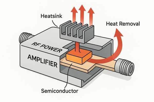
Understanding the Impact of Heat on RF Power Amplifiers
When an RF power amplifier (PA) overheats, several negative things happen. Its gain can drop, the power output can become unstable, and its linearity can suffer, leading to unwanted signal distortion. This is especially true for high-power Gallium Nitride (GaN)1 devices, which pack a lot of power into a small area. I recall a photonic computing chip project at Lightelligence where managing the thermal load of the high-speed interface was critical for the chip's on-time release; even slight overheating could skew results.
The reliability of an electronic device is often measured by its Mean Time Between Failures (MTBF)2. High temperatures drastically reduce MTBF because they accelerate material degradation and electromigration.
| Semiconductor Technology | Typical Max. Junction Temp. (\(T_{j,max}\)) Range (\(\text{°C}\)) | Recommended Operating \(T_j\) for Reliability (\(\text{°C}\)) | Key Considerations |
|---|---|---|---|
| LDMOS | \(150 - 175\) | \(< 150\) | Mature technology, cost-effective for many applications |
| GaN (Gallium Nitride) | \(175 - 225\) | \(< 150 - 175\) (application & manufacturer dependent) | High power density, superior high-frequency performance |
Note: Always consult manufacturer datasheets for specific device ratings and derating guidelines.
Keeping below these limits is a core part of robust design. For instance, while a GaN device might have a \(T_{j,max}\) of \(225 \text{°C}\), many application notes (e.g., from Qorvo or Wolfspeed) emphasize maintaining \(T_j\) well below this, often targeting under \(150 \text{°C}\) for continuous wave (CW) applications to ensure long-term reliability.
What Is the Main Purpose of Thermal Vias Under an RF Component?
Are your critical RF components becoming localized hot spots? This trapped heat needs a quick and efficient escape route. Thermal vias offer a direct path to pull that heat away from the sensitive area.
The main purpose of thermal vias is to create a low thermal resistance path. They effectively transfer heat directly from a hot component on the PCB surface to larger internal or external copper planes, which then act as heatsinks.
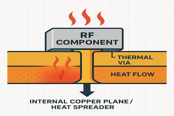
A Closer Look at How Thermal Vias Function
Thermal vias are essentially small, plated holes that go through the PCB, connecting the component's thermal pad on the surface to larger copper areas, usually ground or power planes, or a dedicated thermal plane. Heat, always seeking the path of least resistance, travels down these copper-plated cylinders.
The effectiveness of a thermal via depends on its construction.
| Parameter | Typical Range / Value | Impact on Thermal Performance | Notes |
|---|---|---|---|
| Via Diameter | \(0.2 \text{ mm} - 0.5 \text{ mm (8-20 mils)}\) | Larger diameter lowers individual via resistance | Balance between thermal needs and PCB routing/fabrication constraints. |
| Plating Thickness | \(20 \text{ } \mu\text{m} - 35 \text{ } \mu\text{m+}\) | Thicker plating significantly reduces thermal resistance3 | IPC-6012 Class 2 often specifies min \(20 \text{ } \mu\text{m}\); \(>25 \text{ } \mu\text{m}\) is better for thermal. |
| Via Filling | Unfilled, Conductive Epoxy | Filled vias offer lower resistance than air-filled. | Epoxy \(k \approx 0.5-2 \text{ W/m·K}\). Copper filling offers best performance but is costly. |
| Connection to Plane | Direct, robust stitching | Ensures efficient heat transfer from via to the spreading plane. | Multiple stitches per via if connecting to thin traces. |
Sometimes, these vias are filled with thermally conductive epoxy or even solid copper (though more expensive) to further reduce thermal resistance. The goal is to lower the junction temperature (\(T_j\)) of the component, which directly impacts its performance and lifespan. I've seen many designs where simply adding a well-planned array of thermal vias4 significantly improved device reliability without needing a larger external heatsink.
What Makes a Thermal Via Array Design Effective?
Just scattering some vias under a hot component isn't a guaranteed fix. An poorly designed or sparse via array won't cool effectively. Proper, thoughtful design is absolutely key for achieving good thermal performance.
An effective thermal via array design features multiple vias placed directly under the heat source (the component's thermal pad). It uses optimal spacing, appropriate diameter, and sufficient copper plating to collectively minimize thermal resistance.
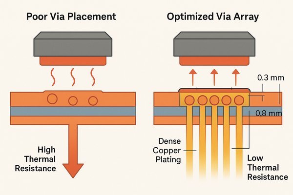
Key Factors for an Effective Thermal Via Array
Several factors contribute to an effective thermal via array. The aim is to maximize heat flow from the component into the larger thermal planes of the PCB.
| Factor | Typical Value/Consideration | Importance for Effectiveness |
|---|---|---|
| Number of Vias | Maximize under thermal pad area | More vias create more parallel paths, lowering overall \(\theta_{JA}\). |
| Via Pitch/Spacing | \(0.8 \text{ mm} - 1.27 \text{ mm (30-50 mils)}\) | Balances thermal path density with PCB manufacturability/integrity. |
| Via Diameter | \(0.2 \text{ mm} - 0.5 \text{ mm}\) | Smaller allows more vias; larger has lower individual resistance. |
| Plating Thickness | \(>25 \text{ } \mu\text{m}\) (e.g., \(1 \text{ oz copper in barrel}\)) | Critical for reducing individual via thermal resistance. |
| Plane Connection | Solid, low-inductance to large plane | Plane acts as the immediate heat spreader; connection quality matters. |
The concept of thermal spreading resistance is also important. The heat needs to spread out from the small footprint of the vias into the larger copper plane. A dense array directly under the heat source is usually most effective. In my experience, especially with high-power density components, simulating the via array performance is a valuable step to avoid discovering problems after the first prototype build.
When Can a PCB Copper Pour Act as an Effective Heatsink?
Are you wondering if that large copper plane on your PCB is doing enough cooling? Sometimes, the PCB itself, with its copper layers, can dissipate a surprising amount of heat. But the question is, how much copper area and thickness are truly enough?
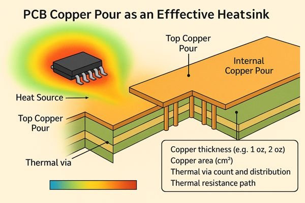
A PCB copper pour acts as an effective heatsink when it has sufficient surface area and thickness (copper weight), and is well-connected to the heat source through low thermal resistance paths, like a good array of thermal vias.
Maximizing Copper's Cooling Potential
Copper is an excellent conductor of heat, with a thermal conductivity5 (\(k\)) around \(385-401 \text{ W/m·K}\). The more copper you have, and the better it's connected to the heat source, the more effectively it can draw heat away and spread it over a larger area for dissipation.
| Copper Weight | Approx. Thickness (\(\mu\text{m}\)) | Relative In-Plane Thermal Resistance (vs. 1 oz baseline \(R_0\)) | Common Thermal Management Role |
|---|---|---|---|
| \(0.5 \text{ oz}\) | \(17.5\) | Higher (approx. \(2 \times R_0\)) | Minimal heat spreading; primarily for signal integrity. |
| \(1 \text{ oz}\) (Std) | \(35\) | Baseline (\(R_0\)) | General purpose; some heat spreading for low/moderate power. |
| \(2 \text{ oz}\) | \(70\) | Lower (approx. \(0.5 \times R_0\)) | Good for power planes; significant improvement in spreading. |
| \(3 \text{ oz}\) | \(105\) | Much Lower (approx. \(0.33 \times R_0\)) | High power applications; excellent lateral heat spreading. |
During the development of some industrial automation modules, we leveraged \(2 \text{ oz}\) copper planes extensively to manage the heat from driver ICs, avoiding the need for individual heatsinks in many cases. This is where the "Thermal-RF Co-Design" concept really shines – using the PCB structure itself as a primary thermal management tool. However, PCB copper pours6 have limitations. For very high-power devices, or in high ambient temperatures, the PCB alone might not be enough.
What RF Device Power Level Typically Necessitates an External Heatsink?
Is your RF device generating so much heat that the PCB alone just can't handle it? There comes a point where an external heatsink becomes essential. But when do you cross that line?
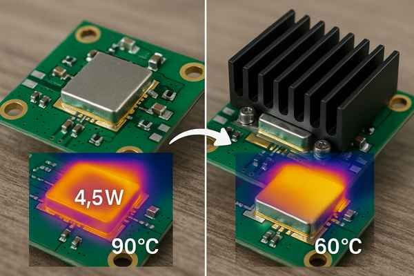
RF devices generating more than a few watts, often in the range of \(2-5 \text{ Watts}\) or higher, typically necessitate an external heatsink. This threshold heavily depends on the application's thermal environment, PCB design, and the component's maximum allowable temperature.
Deciding When an External Heatsink is Necessary
Making the call for an external heatsink involves a thermal budget analysis. A simplified calculation is: \(T_J = T_A + P_D \times \theta_{JA}\). If your calculated \(T_J\) approaches or exceeds \(T_{j,max}\) using only PCB cooling, you need to reduce \(\theta_{JA}\).
| Factor Influencing Heatsink Need | Consideration | Impact on Junction Temp (\(T_j\)) |
|---|---|---|
| Power Dissipation7 (\(P_D\)) | Higher \(P_D\) means more heat to remove. | Directly proportional increase in \(T_j\) for a given \(\theta_{JA}\). |
| Max Junction Temp (\(T_{j,max}\)) | Device-specific limit (e.g., \(150-225 \text{°C}\)). | This is the absolute ceiling; aim to operate well below it. |
| Ambient Temperature (\(T_A\)) | The baseline temperature of the device's surroundings. | A higher \(T_A\) means less headroom for temperature rise. |
| PCB Thermal Design | Effectiveness of vias, copper, materials (determines \(\theta_{JA}\) without heatsink). | A poor PCB thermal design results in a high intrinsic \(\theta_{JA}\). |
| Airflow | Natural or forced convection significantly aids heat removal. | Can substantially lower the effective \(\theta_{JA}\). |
For example, if an RF amplifier dissipates \(10 \text{ W}\), and the PCB can only achieve a \(\theta_{JA}\) of \(15 \text{°C/W}\), in a \(40 \text{°C}\) ambient environment, the junction temperature would be \(40 \text{°C} + 10 \text{ W} \times 15 \text{°C/W} = 190 \text{°C}\). If the device's \(T_{j,max}\) is \(175 \text{°C}\), this is too hot, and a heatsink is needed to lower \(\theta_{JA}\) significantly.
How Is Good Thermal Contact Ensured Between an RF PCB and a Heatsink?
So you've decided to use an external heatsink, but your component temperatures are still higher than expected? Poor thermal contact between the PCB (or component) and the heatsink can severely undermine your cooling efforts.
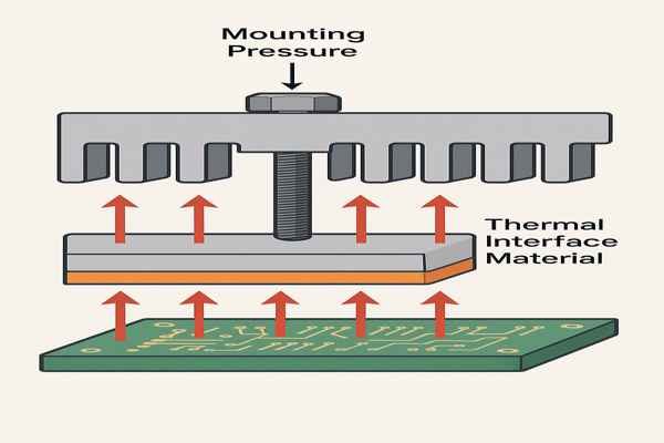
Good thermal contact between an RF PCB and an external heatsink is ensured by using appropriate Thermal Interface Materials (TIMs), applying adequate and even mounting pressure, and ensuring both mating surfaces are clean, flat, and smooth.
Ensuring an Effective Thermal Interface
Even surfaces that appear smooth have microscopic air gaps (air's \(k \approx 0.026 \text{ W/m·K}\)). TIMs fill these, replacing air with a more conductive material.
| TIM Type | Typical Thermal Conductivity (\(\text{W/m·K}\)) | Advantages | Disadvantages |
|---|---|---|---|
| Thermal Grease/Paste | \(0.5 - 12+\) | Very thin bond lines, conforms well to surfaces. | Can be messy, potential for pump-out over time. |
| Thermal Pads | \(0.5 - 20+\) | Easy to apply, consistent thickness, often reusable. | Generally higher thermal resistance due to thickness. |
| Phase Change Mats (PCMs) | \(2 - 6+\) | Flows at operating temp for thin bond line, reliable. | Requires specific activation temperature. |
| Graphite Pads/Sheets | e.g., \(X,Y: 500-1500\)* | Very high in-plane \(k\), durable, no pump-out. | Can be electrically conductive, more rigid. |
| Thermal Adhesives/Tapes | \(0.5 - 3\) | Provides both adhesion and thermal interface. | Often lower \(k\), can be difficult to rework. |
*Highly anisotropic; Z-axis (through-plane) conductivity for graphite sheets is much lower (e.g., \(5-30 \text{ W/m·K}\)).
Beyond TIMs, mounting pressure8 from screws or clips is critical to compress the TIM. Ensure surfaces are flat and clean. Any warping or debris increases thermal resistance.
Which PCB Material Property Signifies Good Heat Transfer Capability?
When you're selecting PCB materials for high-power RF applications, electrical properties like dielectric constant and loss tangent are usually top of mind. However, overlooking the thermal properties can lead to serious overheating issues down the line.
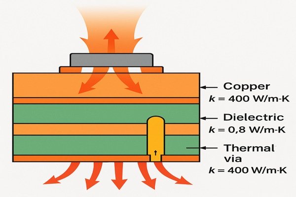
The key PCB material property that signifies good heat transfer capability is its thermal conductivity, typically denoted as \(k\). It's measured in Watts per meter-Kelvin (\(\text{W/m·K}\)). A higher \(k\) value means better heat conduction.
Key Material Properties for Heat Transfer
Different PCB materials have vastly different thermal conductivities (\(k\)). Higher \(k\)-values are generally better for heat dissipation.
| PCB Material Type | Example Material(s) | Typical \(k\) (\(\text{W/m·K}\)) | Notes |
|---|---|---|---|
| Standard FR-4 | Generic FR-4 | \(0.25 - 0.35 \text{ (through-plane)}\) | Low cost, common, poor thermal conductor. |
| RF Laminate (Hydrocarbon) | Rogers RO4350B | \(\approx 0.69 \text{ (z-axis), } \approx 0.93 \text{ (x,y-axis)}\)* | Good RF performance, moderate \(k\). |
| RF Laminate (PTFE) | Rogers RO3003 | \(\approx 0.50 \text{ (isotropic)}\)* | Excellent RF properties, moderate \(k\). |
| IMS Dielectric | Bergquist Thermal Clad etc. | \(1 - 3+\) | For Metal Core PCBs (MCPCBs)9, designed for good \(k\). |
| IMS Base (Aluminum) | Aluminum (e.g., 6061) | \(\approx 167\) | Excellent heat spreader, integral part of MCPCB. |
| IMS Base (Copper) | Copper (e.g., C110) | \(\approx 390\) | Superior heat spreading, higher cost/weight than aluminum in MCPCBs. |
() Values are typical and can vary by specific product grade; always refer to manufacturer datasheets like those from Rogers Corporation or Isola for precise figures.*
The thickness of dielectric layers also plays a role; thinner dielectrics generally mean lower thermal resistance. This is another area where "Thermal-RF Co-Design" is critical, selecting materials not just for RF specs but as an integral part of the thermal solution.
How Does Increased PCB Copper Weight Aid Thermal Management?
You might be considering using thicker copper (higher copper weight) on your PCB traces and planes, primarily for handling higher currents. But did you know it also offers significant benefits for thermal management?
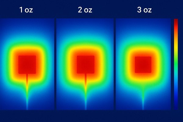
Increased PCB copper weight, such as using \(2 \text{ oz } (70 \text{ } \mu\text{m})\) or \(3 \text{ oz } (105 \text{ } \mu\text{m})\) copper instead of the standard \(1 \text{ oz } (35 \text{ } \mu\text{m})\), directly improves thermal management. It reduces thermal resistance within the copper layers and thermal vias, enhancing lateral heat spreading and improving heat conduction to heatsinks or cooler areas of the board.
Leveraging Heavier Copper for Cooling
Heavier copper has a direct, positive impact on thermal pathways by increasing the cross-sectional area for heat flow.
| Copper Feature | Impact of Increased Copper Weight (e.g., \(1 \text{ oz to } 2 \text{ oz}\)) | Primary Thermal Benefit |
|---|---|---|
| Traces | Lower electrical and thermal resistance. | Reduced \(I^2R\) self-heating; better local heat conduction along trace. |
| Planes (Solid) | Significantly lower in-plane thermal resistance. | Improved lateral heat spreading; reduces temperature gradients. |
| Via Barrels | Increased copper cross-section in via plating. | Lower individual via thermal resistance, better heat sinking. |
| Component Pads | Better heat sinking at component lead/pad interface. | More efficient heat extraction directly from the component body. |
During the design of a power supply unit for a medical device, we opted for \(3 \text{ oz}\) copper on specific layers. This was primarily for current carrying, but the improved thermal performance was a significant secondary benefit. While IPC-2152 gives guidance on current capacity (related to thermal limits), the direct benefit of thicker copper for heat spreading is fundamental.
Can Placing Hot RF Components Far Apart Improve Board Cooling?
You have multiple components on your RF PCB that are generating significant heat. An intuitive approach might be to spread them out as much as possible. But does this spacing strategy actually help in cooling the board more effectively?
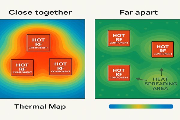
Yes, generally, placing hot RF components far apart can improve overall board cooling. This strategy helps by reducing thermal coupling between components and allowing each individual component more adjacent PCB area for heat spreading and convection, thus preventing the formation of concentrated, intense hot zones.
Benefits of Strategic Component Placement
When heat-generating components are close, their thermal plumes interact, reducing individual cooling. Spacing them out offers several advantages:
| Aspect of Component Spacing | Benefit for Cooling | Potential Trade-off / Consideration |
|---|---|---|
| Reduced Thermal Coupling10 | Prevents one component from excessively heating another. | May increase trace lengths, impacting high-speed signals. |
| Increased Spreading Area | Each component gets more local PCB for heat dissipation. | Can lead to larger overall PCB size if not managed carefully. |
| Improved Airflow Access | Better natural or forced convection for each part. | May not be beneficial if overall chassis airflow is poor or obstructed. |
| Easier Heatsink Mounting | More space for individual heatsinks if needed. | --- |
In my work on elevator control systems, ensuring adequate spacing between power resistors and sensitive control ICs was crucial for long-term system stability. However, electrical performance (e.g., short paths for critical signals) always needs to be balanced with thermal considerations.
What Benefit Does Thermal Simulation Offer for RF PCB Design?
Are you still relying on educated guesses or "rules of thumb" to predict if your RF PCB will overheat? In today's complex designs, thermal simulation tools can predict and help prevent serious heat-related problems long before you even order the first prototype.
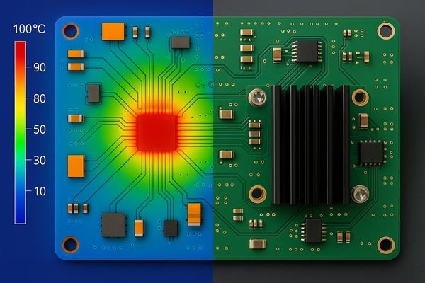
Thermal simulation offers immense benefits by predicting temperature distributions across the RF PCB under operational loads. It identifies potential hot spots and allows engineers to virtually evaluate and compare different cooling strategies, thereby optimizing thermal performance early in the design cycle.
The Power of Thermal Simulation in RF Design
Thermal simulation software (using FEA or CFD) models heat transfer based on physics. Accurate inputs lead to insightful outputs.
| Thermal Simulation Aspects | Examples / Details | Purpose / Benefit |
|---|---|---|
| Key Inputs | Material \(k\)-values, component \(P_D\), ambient conditions (\(T_A\), airflow), PCB layout, 3D CAD models. | Define the thermal problem accurately for realistic simulation. |
| Analysis Performed | Solves for conduction, convection, radiation heat transfer. | Predicts how heat moves through the system based on physical principles. |
| Key Outputs | Temperature maps (\(T_j\), \(T_C\)), airflow patterns, heat flux vectors. | Visualize thermal performance, identify hot spots, assess cooling strategy effectiveness. |
| Primary Benefits | Early problem ID, design optimization, fewer prototype iterations, improved reliability. | Make informed decisions, reduce costs, and ensure product robustness before build. |
This is where the "Thermal-RF Co-Design" approach, which I'm a strong advocate for, truly comes into its own. Simulation allows us to treat the PCB's substrate, copper planes, and via structures as integral parts of the thermal solution from the outset. This holistic view is crucial for high-power density designs, especially with GaN devices.
Conclusion
Effectively cooling high-power RF PCBs demands a comprehensive strategy. It involves careful material selection, smart use of thermal vias and copper, and sometimes, external heatsinks. Early thermal simulation and a co-design mindset are your best allies for success.
-
GaN technology offers high power density and efficiency, making it essential for modern RF applications. Discover its benefits here. ↩
-
Understanding MTBF is crucial for assessing the reliability of electronic devices, especially in high-temperature environments. Explore this link to learn more. ↩
-
Exploring thermal resistance helps in optimizing PCB designs for better heat dissipation and overall performance. ↩
-
Understanding thermal vias is crucial for effective PCB design, as they significantly impact heat management and device reliability. ↩
-
Understanding thermal conductivity is crucial for optimizing heat management in various applications, including electronics and industrial processes. ↩
-
Learning about PCB copper pours can help you design better thermal solutions in electronics, maximizing efficiency and reliability. ↩
-
Exploring the impact of Power Dissipation helps in designing efficient cooling solutions for electronic components, preventing overheating. ↩
-
Learn about the significance of mounting pressure in ensuring effective thermal contact and reducing thermal resistance in your setups. ↩
-
Explore the benefits of MCPCBs for efficient heat management in electronic designs. ↩
-
Understanding Reduced Thermal Coupling can help you design better cooling systems for electronic components, enhancing performance and longevity. ↩


