Struggling with RF prototypes that don't work? Wasting time and money on endless board spins? Getting RF designs right the first time can feel like a constant battle.
Preventing major RF PCB prototyping errors involves a proactive approach: meticulous planning, early simulation of critical RF paths using 3D EM solvers, careful component selection and footprint verification, adherence to grounding best practices, and thorough post-assembly testing before extensive validation.

I've seen my share of RF projects go sideways, and it's often the early-stage oversights that cause the biggest headaches. The key is to treat electromagnetic (EM) considerations not as an afterthought, but as a foundational part of your design process from day one. By "de-risking" the design through simulation and careful verification before you even think about sending Gerbers out for fabrication, you can save yourself a world of trouble. Let's dive into how you can avoid some common pitfalls and get your RF prototypes working sooner.
What Common RF Design Oversight Leads to Failed Prototypes?
Feeling the pain of another failed RF prototype? Wondering what simple mistake could be derailing your project schedule and budget? It's a common frustration in RF engineering.
A frequent and critical RF design oversight leading to failed prototypes is the inadequate characterization and modeling of parasitic effects associated with passive components, PCB traces, vias, and connectors at the intended operating frequencies.
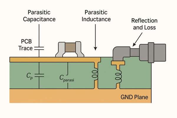
In RF design, especially as frequencies climb into the GHz range, elements you might safely ignore in lower-frequency digital or analog designs suddenly become dominant players. It's not just about the ideal behavior of your components; it's how they interact with the physical environment of the PCB.
Understanding Component Parasitics
Passive components like capacitors, inductors, and resistors are not ideal. A capacitor has some series inductance (\(ESL\)) and series resistance (\(ESR\)). An inductor has parallel capacitance. These parasitics can dramatically alter a component's behavior at RF. For instance, a capacitor can become self-resonant, acting like an inductor above its self-resonant frequency (\(SRF\)). I remember a project where a seemingly simple filter circuit performed abysmally in the first prototype. The issue wasn't the textbook filter design itself, but the unacknowledged parasitic capacitance1 of the pads and the inductance of the short traces connecting the SMT components. At 2.4 GHz, these "minor" parasitics significantly shifted the filter's response.
The Impact of Layout Parasitics
Beyond discrete components, the PCB layout itself introduces parasitics. These are unintended capacitances, inductances, or resistances that arise from the physical arrangement of conductors and dielectrics.
| Parasitic Element | Typical RF Impact | Common Mitigation Strategy |
|---|---|---|
| Capacitor \(ESL\) | Shifts self-resonant frequency (\(SRF\)) lower, acts inductive above \(SRF\) | Choose capacitors with high \(SRF\), use smaller package sizes |
| Inductor Parallel Capacitance | Shifts \(SRF\) lower, creates unintended resonance | Select inductors with high \(SRF\), consider shielded inductors |
| Via Inductance | Degrades impedance match, can cause signal reflections, ground bounce | Use multiple vias for low inductance, keep vias short, consider microvias |
| Trace-to-Trace Capacitance | Crosstalk, unintended coupling | Maintain sufficient spacing between traces (e.g., \(3 \times \text{width}\) rule) |
| Pad Capacitance | Detunes matching networks, alters filter responses | Accurate footprint design, EM simulation of pads |
Overlooking these subtle, frequency-dependent behaviors is a classic route to a non-functional prototype. It's crucial to consult component datasheets for S-parameters or parasitic models if available, and to use EM simulation tools to understand layout effects.
Why Is Verifying RF Component Footprints Before Layout So Critical?
Ever had an RF prototype arrive with components that don't fit, or worse, fit but perform poorly? This frustrating issue often traces back to unverified footprints, creating costly delays.
Verifying RF component footprints before layout is critical because incorrect pad sizes, spacing, or land patterns can introduce significant impedance mismatches, signal reflections, and parasitic reactances, severely degrading RF performance or preventing assembly.
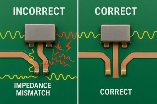
I can't stress this enough: RF component footprints are not just about whether the part will physically sit on the board; they are an integral part of the RF circuit.
Beyond Physical Fit: Electrical Performance
For RF circuits, the footprint directly influences the local electromagnetic field and, therefore, the component's performance.
- Pad Parasitics: The size and shape of component pads contribute capacitance to ground and mutual capacitance to adjacent pads. Incorrect pad dimensions can detune matching networks or filters.
- Transition to Traces: The way a component pad transitions to a PCB trace affects impedance. An abrupt change in width can cause reflections.
I recall an incident early in my career involving a high-frequency amplifier. The datasheet specified a particular land pattern, but the library part used had slightly narrower pads. The result? Increased parasitic capacitance at the input and output, leading to instability and oscillations that weren't predicted by simulations using ideal component models.
Adherence to Standards and Manufacturer Recommendations
While IPC-7351C (Generic Requirements for Surface Mount Design and Land Pattern Standard)2 provides excellent general guidelines, RF often requires more.
- Manufacturer Datasheets: Always prioritize the land pattern recommendations in the RF component's datasheet. Manufacturers often optimize these for high-frequency performance.
- Application Notes: Look for application notes that discuss PCB layout for specific RF parts or families. These can provide invaluable insights.
For example, a QFN package for an RFIC might have very specific requirements for via stitching under the thermal/ground pad and precise pad dimensions to control the transition from the package to the PCB trace. Getting this wrong can mean a \(>3\text{dB}\) loss in power or a significant shift in resonant frequency. Always cross-verify library footprints against the latest datasheet.
| Footprint Aspect | Potential RF Impact if Incorrect | Recommendation |
|---|---|---|
| Pad Width/Length | Impedance mismatch, parasitic capacitance/inductance | Follow datasheet strictly, simulate if deviating |
| Pad Spacing | Coupling, crosstalk, impedance issues | Adhere to datasheet and assembly clearance rules |
| Solder Mask Opening | Affects capacitance, solderability | Match pad size or slightly larger as per standards |
| Thermal/Ground Pad Vias | Poor grounding, thermal issues, altered impedance | Use multiple small vias, follow datasheet layout |
How Can RF Simulations Reduce Prototype Board Spins?
Tired of the endless cycle of RF prototype, test, fail, redesign, and respin? Each iteration costs time and money, pushing your project further behind schedule. There must be a better way.
RF simulations, particularly 3D electromagnetic (EM) modeling, reduce prototype board spins by allowing engineers to predict and optimize circuit performance, identify potential issues like impedance mismatches or unwanted resonances, and validate design choices virtually before fabrication.
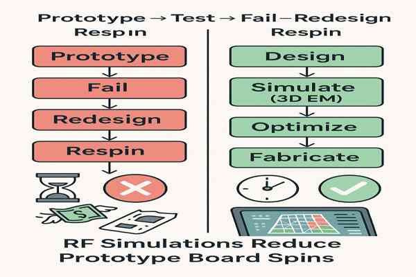
Simulations are your crystal ball in RF design, offering a chance to "test" your design before you even order a PCB.
The Power of Electromagnetic Modeling
EM simulation tools (like ANSYS HFSS, CST Studio Suite, or Keysight Momentum) solve Maxwell's equations for your specific geometry and materials. This allows you to:
- Visualize Fields: See how E-fields and H-fields behave in your structure, identifying areas of high coupling or radiation.
- Extract S-parameters3: Predict how your circuit will perform in terms of gain, loss, reflection, and isolation across a frequency range.
- Optimize Geometries: Tweak trace widths, spacings, via placements, etc., in software to achieve desired performance.
I worked on a project involving a compact antenna matching network. Without EM simulation, we would have likely needed at least two or three spins to get the match right. Using a 3D EM solver, we modeled the exact trace geometries, substrate properties, and even the SMT component parasitics. The simulation showed us that our initial layout had a 2 dB insertion loss due to an unexpected coupling path. We adjusted the layout in the software, re-simulated, and the first physical prototype performed within 0.5 dB of the simulated results. This saved us weeks.
From Ideal to Reality: Modeling Non-Idealities
The key to effective simulation is modeling the physical reality. This involves more than just ideal components.
| Simulation Type | Primary Use Case | Key Outputs |
|---|---|---|
| 3D EM Full-Wave (e.g., HFSS, CST) | Antennas, complex 3D structures, connectors, package modeling, radiation | S-parameters, radiation patterns, field distributions, impedance |
| 2.5D Planar EM (e.g., Momentum) | Planar filters, couplers, transmission lines, discontinuities on PCBs | S-parameters, impedance, current distributions |
| Circuit Simulation (with EM models) | System-level analysis, matching networks, amplifier stability using S-parameters | Gain, noise figure, \(P_{1\text{dB}}\), \(IP_{3}\), stability factors, transient response |
| Co-simulation (EM + Circuit) | Accurate analysis of circuits with critical EM components (e.g., IC on PCB) | Combines accuracy of EM with speed of circuit simulation for complex systems |
It's essential to use accurate substrate properties (\(D_{k}\), \(D_{f}\)), component models (S-parameters or parasitic models), and model connectors and launches precisely. A typical workflow might involve simulating critical sections first, then integrating these models into a larger circuit or system simulation.
What Happens If an Unsuitable PCB Material Is Used for an RF Prototype?
Have you ever had an RF prototype that performs wildly different from simulations, despite a carefully designed circuit? The culprit might be hiding in your PCB stack-up – the material itself.
Using an unsuitable PCB material for an RF prototype can lead to excessive signal loss, unpredictable impedance variations, and frequency-dependent performance degradation due to inappropriate dielectric constant (\(D_{k}\)) or high dissipation factor (\(D_{f}\)).
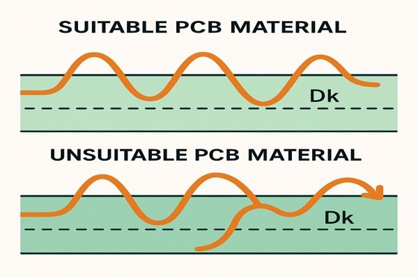
PCB material selection is foundational for RF success. What works for a digital board can be a disaster for RF.
Key Material Properties for RF
Two primary parameters govern an RF laminate's suitability:
- Dielectric Constant4 (\(D_{k}\) or \(\epsilon_{r}\)): Affects the impedance of transmission lines and the physical size of distributed components (like patch antennas or microstrip filters). A stable \(D_{k}\) across frequency and temperature is crucial for predictable performance.
- Dissipation Factor5 (\(D_{f}\) or \(\tan \delta\)): Represents the signal loss within the dielectric material. A lower \(D_{f}\) means less attenuation, especially important at higher frequencies or for long signal paths.
I learned this the hard way on an early Wi-Fi project. We prototyped on generic FR-4. Signal strength was low, and antenna tuning was off. The FR-4's \(D_{k}\) varied, and its \(D_{f}\) was high (around 0.020-0.025). Specialized RF materials like Rogers RO4350B6 (\(D_{f} \approx 0.0037\) at 10 GHz, as per their datasheet) offer much better performance.
Common RF Laminate Choices
| Material Type | Typical \(D_{k}\) Range | Typical \(D_{f}\) (@10GHz) | Pros | Cons |
|---|---|---|---|---|
| FR-4 | 4.0 - 4.8 | 0.015 - 0.025 | Low cost, widely available | High loss, \(D_{k}\) varies with frequency |
| Rogers RO4000 series | 2.55 - 6.15 | 0.002 - 0.004 | Good RF performance, stable \(D_{k}\) | Higher cost than FR-4 |
| Rogers RT/duroid series | 2.2 - 10.2 | 0.0009 - 0.003 | Excellent RF performance, very stable | Very high cost, specialized processing |
| Isola IS680 | 3.0 - 3.45 | 0.0025 - 0.0035 | Good for high-speed digital & some RF | Mid-to-high cost |
| Panasonic Megtron | 3.3 - 3.8 | 0.002 - 0.004 | Very low loss, stable \(D_{k}\) | High cost |
Note: \(D_{k}\) and \(D_{f}\) values are approximate and vary with specific material grade and frequency. Always consult manufacturer datasheets.
Impact on Design
If your design relies on precise 50-Ohm traces, an unexpected \(D_{k}\) shift from 4.3 to 4.8 can change the impedance enough to cause significant reflections. High loss directly attenuates your signal, reducing range or sensitivity. For prototypes, it's often worth spending a bit more on a known, characterized RF substrate to ensure your measurements reflect your design, not material inconsistencies.
How Can Misreading an RF Component Datasheet Affect a Prototype?
Ever stared at a non-working RF prototype, wondering how your carefully calculated design could go so wrong? Sometimes, the devil is in the details of a component datasheet you thought you understood.
Misreading an RF component datasheet, such as overlooking specific layout guidelines, misinterpreting impedance matching requirements, or underestimating power handling limits, can directly lead to a dysfunctional or damaged prototype.
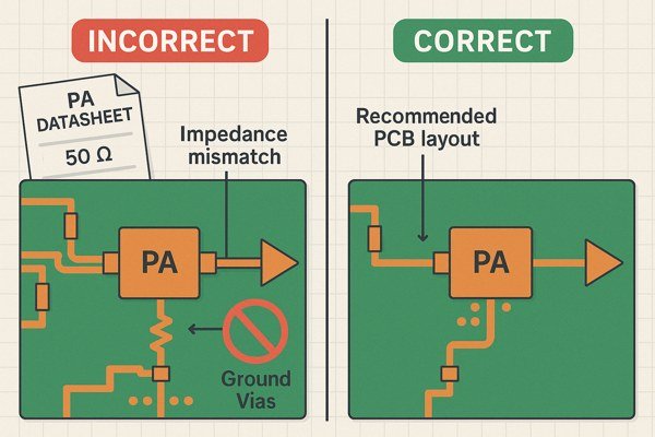
RF component datasheets are dense with critical information, and even a subtle misinterpretation can lead to significant prototype problems.
Critical Information Often Overlooked
My team once faced an LNA prototype with terrible noise figure. The issue? A bypass cap was 5mm away from the Vcc pin, not the recommended \(<2\text{mm}\) in the datasheet, introducing enough parasitic inductance to compromise stability. Datasheets are packed with such critical details.
| Datasheet Section | Key Information to Look For | Potential Impact if Ignored |
|---|---|---|
| Absolute Maximum Ratings | Voltage, current, power limits, temperature ranges | Permanent component damage |
| Electrical Characteristics | Gain, noise figure, \(P_{1\text{dB}}\), \(IP_{3}\), frequency range, matching S-parameters, current consumption | Performance not meeting specs, unexpected behavior |
| Pin Descriptions | Function of each pin, special requirements (e.g., "NC" might mean "Do Not Connect" or "Must Ground") | Incorrect circuit operation, damage if misconnected |
| Layout Guidelines | Recommended footprint, via placement, grounding techniques, trace routing near component | Poor RF performance, instability, thermal issues |
| Typical Application Circuit | Component values for matching, biasing, decoupling; PCB stack-up used for evaluation board | Suboptimal performance if blindly copied without adaptation |
| Thermal Information | Thermal resistance (\(\theta_{JC}\), \(\theta_{JA}\)), power dissipation limits, heatsinking requirements | Overheating, reduced lifespan, performance degradation |
| Packaging Information | Footprint dimensions, pad layout, moisture sensitivity level (MSL) | Assembly issues, poor solder joints, component damage from moisture |
Decoding Application Circuits
The "typical application circuit" is a great starting point, but it's not a plug-and-play solution. Understand why specific components or layout choices were made. For example, matching networks are often frequency-specific and substrate-dependent. You must adapt them to your specific PCB stack-up and operating conditions. Always scrutinize every detail, and when in doubt, contact the manufacturer's application support.
What Is a Common RF Grounding Mistake In Early Prototypes?
Is your RF prototype plagued by noise, instability, or mysterious emissions? A surprisingly common culprit lurks in how you've handled your ground connections, a critical aspect often underestimated in early designs.
A common RF grounding mistake in early prototypes is providing an inadequate or high-impedance return path for RF currents, often due to insufficient ground vias, fragmented ground planes, or long, inductive ground traces.
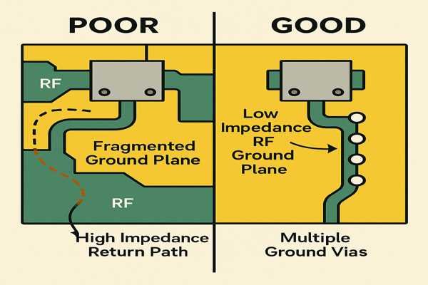
Ground is not just a DC reference in RF circuits; it's an active and critical part of the high-frequency signal path.
The Importance of Low-Impedance Return Paths
At RF frequencies, currents follow the path of least inductance, not necessarily the path of least resistance. For a microstrip line, this means the return current wants to flow in the ground plane directly beneath the signal trace.
- Solid Ground Planes: Avoid slots or large cutouts in the ground plane under or near RF traces. These can force return currents to take detours, increasing inductance and creating potential radiation loops.
- Via Stitching: When RF signals transition between layers, or when connecting component ground pads to the main ground plane, a robust via connection is essential. I worked on a project with an RF switch that showed unexpected signal leakage between ports. The issue was traced to sparse via stitching7 around the switch. A single via can have 0.5 nH to 1 nH of inductance. For good RF grounding, especially around component pads or along the edges of ground fills, a common rule of thumb is to place vias at intervals of \(\frac{\lambda}{20}\) to \(\frac{\lambda}{8}\) (where \(\lambda\) is the wavelength of the highest operating frequency in the substrate). For 5 GHz on FR-4 (\(D_{k} \approx 4.3\)), \(\lambda\) is roughly 28mm, so \(\frac{\lambda}{20}\) is about 1.4mm. Vias should ideally be much closer in critical areas.
Common Grounding Pitfalls
| Mistake | Consequence | Solution |
|---|---|---|
| Fragmented/Split Ground Planes (unintentionally) | Increased return path inductance, noise coupling, unpredictable impedances | Use solid ground planes under RF sections where possible, manage splits carefully |
| Insufficient Vias for Ground Connections | High impedance ground, poor component performance, ground bounce8 | Use multiple vias ("via stitching") for all RF component ground pads and plane connections |
| Long Ground Traces for Components | Inductive ground path, common impedance coupling, increased noise | Connect components directly to the ground plane with short, wide traces or vias |
| Mixing Noisy Digital Grounds with Sensitive RF Grounds | Noise injection into RF circuitry, desensitization | Careful partitioning, consider ground separation with a single-point bridge if necessary, use ferrite beads for isolation |
| Floating Metal Structures | Unintended resonance, parasitic coupling, radiation | Ensure all conductive elements (shields, heatsinks, unused pads) are properly grounded |
Proper grounding also involves ensuring all metallic enclosures or shields are well-bonded to the RF ground to prevent them from acting as unintended antennas.
Why Is It Vital to Consider RF Trace Behavior Even for Prototypes?
Think RF trace impedance and signal integrity are only for final production boards? Overlooking these critical aspects in your RF prototypes can lead to misleading test results and unnecessary redesigns.
It's vital to consider RF trace behavior (impedance, loss, coupling) even for prototypes because these characteristics directly impact signal power transfer, integrity, and circuit performance, determining if the prototype accurately reflects the intended design.
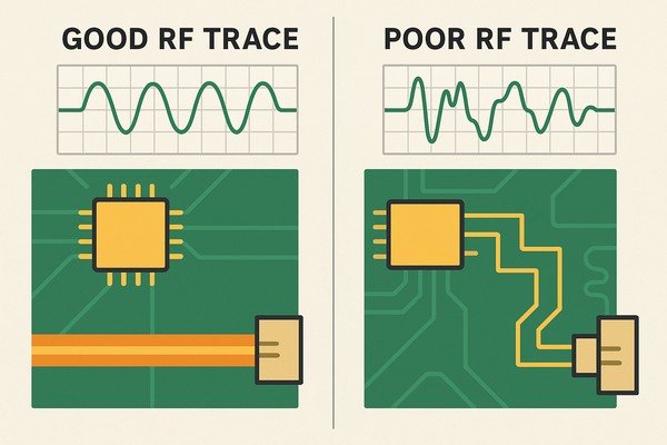
Even for a "quick and dirty" prototype, RF traces are not just simple connections; they are transmission lines. Their physical characteristics are paramount.
Characteristic Impedance9 (\(Z_{0}\))
The characteristic impedance (\(Z_{0}\)) of a trace is determined by its physical dimensions and the PCB material properties.
- Impact of Mismatch: Most RF systems are standardized to 50 Ohms. If a trace meant to be 50 Ohms is actually 40 Ohms or 60 Ohms, this impedance mismatch causes signal reflections. These reflections result in power loss (return loss), signal distortion, and can even affect the stability of active devices like amplifiers.
- Calculation and Control: Tools like Saturn PCB Toolkit or online calculators can help estimate the required trace width. For instance, a 50-ohm microstrip on a 1.6mm thick FR-4 with a \(D_{k}\) of 4.3 might require a trace width of approximately 2.9-3.0 mm.
Key Trace Parameters and Their Influence
| Trace Parameter | Primary Influence On | Design Consideration |
|---|---|---|
| Trace Width (\(W\)) | Characteristic Impedance (\(Z_{0}\)), Current Carrying Capacity, Loss | Adjust \(W\) for target \(Z_{0}\) based on substrate height and \(D_{k}\). Wider for lower loss. |
| Dielectric Height (\(H\)) | Characteristic Impedance (\(Z_{0}\)) | Critical for impedance control. Thicker dielectric often means wider traces for same \(Z_{0}\). |
| Dielectric Constant (\(D_{k}\)) | Characteristic Impedance (\(Z_{0}\)), Propagation Speed, Wavelength | Lower \(D_{k}\) generally leads to wider traces for same \(Z_{0}\). Critical for filters. |
| Copper Thickness (\(t\)) | Loss (Skin Effect), Current Carrying Capacity | Thicker copper reduces conductor loss, especially at lower RF frequencies. |
| Trace Spacing (\(S\)) | Crosstalk (Coupling), Differential Impedance | Maintain \(S > 3W\) to minimize crosstalk. Critical for differential pairs. |
| Trace Length | Overall Loss, Phase Shift, Delay | Keep RF traces as short as possible. Critical for delay lines and phase matching. |
Ignoring these factors in a prototype means you're not truly testing your intended design, potentially leading to false conclusions about component performance or circuit topology.
How Can Poor Prototype Soldering Impact RF Circuit Testing?
You’ve got your RF prototype back, components are placed, but the circuit isn’t working as expected. Before blaming the design, consider a more fundamental issue: the quality of the soldering.
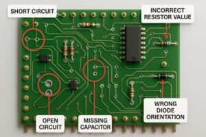
Poor prototype soldering, including cold joints, solder bridges, incorrect component orientation, or excessive solder, can introduce unintended impedances, open circuits, shorts, or parasitic effects, drastically skewing RF circuit testing results.
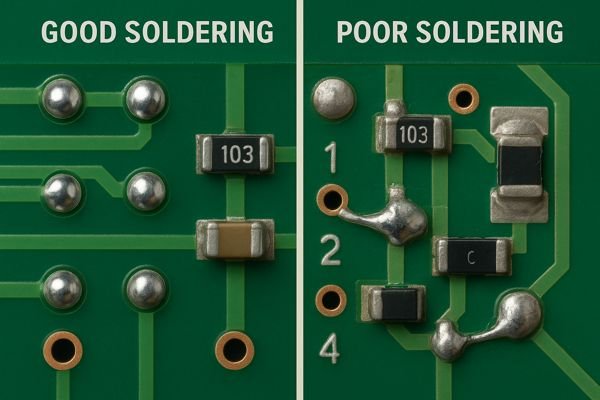
Soldering for RF circuits, especially with tiny Surface Mount Technology (SMT) components and fine-pitch packages, is far more critical than for many other types of electronics.
Common Soldering Defects and Their RF Consequences
The IPC-A-610 (Acceptability of Electronic Assemblies)10 standard provides detailed criteria for solder joint quality. Deviations can severely impact RF performance:
| Soldering Defect | Typical RF Consequence | Visual Cue |
|---|---|---|
| Cold Joint11 | High insertion loss, intermittent connection, noise, instability | Dull, grainy appearance, poor wetting, possible cracks |
| Solder Bridge12 | Short circuit, unintended signal paths, component damage | Solder connecting adjacent pads/pins |
| Excessive Solder | Parasitic capacitance, detuning of sensitive circuits, potential for bridging | Large, bulbous solder joints |
| Insufficient Solder | Open circuit, high resistance, poor mechanical strength, tombstoning | Minimal solder, poor wetting, exposed pads/leads |
| Component Misalignment | Altered impedance, poor connection, detuning, stress on solder joints | Component not centered on pads, skewed, or billboarded |
| Tombstoning | Open circuit for one terminal of a 2-pin component | Component standing on one end |
| Solder Balls/Splatter | Potential for shorts, EMI issues | Small spheres of solder on PCB surface or between components |
| Voiding (esp. under pads) | Poor thermal transfer (for PAs), compromised ground connection, altered impedance | Not easily visible without X-ray, but can cause overheating |
I once spent days debugging an RF receiver prototype with almost no sensitivity. A microscopic inspection revealed a tiny crack in a solder joint on an input matching capacitor – a classic cold joint. Always visually inspect every solder joint under magnification before powering up an RF prototype.
What Initial RF Tests Validate a Prototype's Basic Operation?
Your new RF prototype is on the bench, powered up, and not smoking – that's a good start! But what are the first crucial RF tests to confirm it’s basically alive and well?
Initial RF tests to validate a prototype's basic operation typically include DC power checks, followed by S-parameter measurements (\(S_{11}\) for return loss/input match, \(S_{21}\) for gain/insertion loss) using a Vector Network Analyzer (VNA).
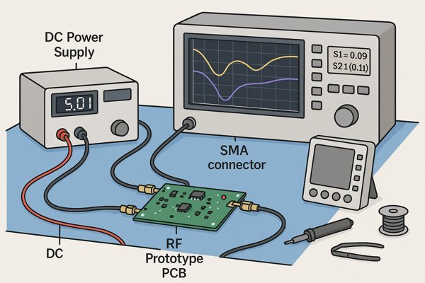
Before diving into complex system-level characterization, you need to confirm that the fundamental RF building blocks are behaving as expected.
Step 1: DC Sanity Checks (The "No Smoke" Test)
This is non-negotiable: verify DC conditions before any RF power is applied. This includes visual inspection for assembly errors, DMM checks for shorts, and careful power-up to verify voltages and quiescent currents at key test points. An unexpectedly high current draw is a red flag.
Step 2: Basic RF Path Verification with a VNA
A Vector Network Analyzer13 is your best friend here.
| Test Type | Key Parameter Measured | Typical "Good" Indication (Example) | Typical "Bad" Indication (Example) |
|---|---|---|---|
| DC Power Check | Voltage (\(V\)), Current (\(A\)) | Voltages within spec (e.g., \(3.3\text{V} \pm 5\%\)), quiescent current as expected | No voltage, low/high voltage, excessive current draw |
| \(S_{11}\) (Return Loss) | Port Impedance Match | \(< -10 \text{ dB}\) (\(\text{VSWR} < 2:1\)) across band | \(> -5 \text{ dB}\) (\(\text{VSWR} > 3.5:1\)), sharp dips/peaks out of band |
| \(S_{21}\) (Gain/Loss) | Signal Transfer | Expected gain (e.g., LNA \(+15\text{dB}\)) or loss (Filter \(-2\text{dB}\)) across band | Significantly lower/higher gain/loss, unexpected frequency response |
| \(S_{22}\) (Return Loss) | Output Port Match | \(< -10 \text{ dB}\) across band | \(> -5 \text{ dB}\) across band |
| \(S_{12}\) (Isolation) | Reverse Signal Leakage | High value (e.g., \(< -20\text{dB}\) for switch, \(< -30\text{dB}\) for amp) | Low value (e.g., \(> -10\text{dB}\)), indicating poor isolation/potential instability |
My typical VNA sweep covers a frequency range wider than the intended operational band to spot any out-of-band issues or unexpected resonances.
Step 3: Basic Spectrum Analysis (If Applicable)
If the prototype involves an oscillator (e.g., a VCO or PLL), or if you suspect self-oscillation in an amplifier, a spectrum analyzer14 is used to verify the output frequency, check for spurs and harmonics, and get a qualitative look at phase noise.
These initial tests provide a baseline and help catch major design or assembly flaws early, saving a lot of time in the long run.
What Documentation Step Aids Iterating From RF Prototype to Production?
So, your RF prototype works, or perhaps it needs a few tweaks. How do you ensure the lessons learned from this spin smoothly translate into a successful production version?
Thoroughly documenting all design changes, component substitutions, test results (both good and bad), and layout modifications made during the prototype phase is the critical documentation step for efficient iteration to production.
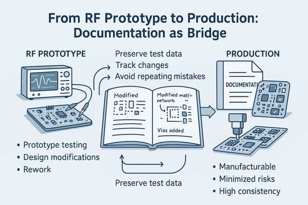
The journey from a working (or semi-working) RF prototype to a mass-producible product hinges on meticulous record-keeping and a structured approach to managing changes.
Core Elements of Prototype Documentation
This isn't just about filing away schematics; it's about creating a comprehensive record of the prototype's life. This includes version-controlled design files (schematics, layout, BOM), detailed test plans and reports (procedures, results, pass/fail criteria compared to simulations), and a log of all modifications.
Tracking Modifications and Lessons Learned
This is where the "iteration" part comes in. A modification log is essential.
| Mod ID | Date | Board S/N | Issue Observed | Modification Made | Test Result (Post-Mod) | Next Spin Action |
|---|---|---|---|---|---|---|
| M001 | 2025-05-23 | P01-001 | Filter center freq too low (2.3GHz) | C5 changed from 2.2pF to 1.8pF | Center freq now 2.42GHz | Update C5 in schematic/layout |
| M002 | 2025-05-24 | P01-001 | LNA oscillates with input \(> -10\text{dBm}\) | Added 10 Ohm resistor in series with gate bias | Stable up to \(0\text{dBm}\) input | Add R_gate to schematic |
| M003 | 2025-05-25 | P01-002 | PA output power 3dB below target | Inspected solder on PA. Reflowed PA ground paddle. | Output power now at target. | Review stencil for PA ground. |
This disciplined approach ensures that valuable knowledge gained during prototyping isn't lost and directly informs design improvements, making the transition to a reliable production unit much smoother and faster. It forms the basis for your Design Verification Test (DVT) report and feeds into manufacturing guidelines.
Conclusion
Preventing major RF prototyping errors boils down to diligence: simulate early, verify components meticulously, respect material properties and grounding, test thoroughly, and document everything. This saves costly respins.
-
Parasitic capacitance can alter circuit behavior at high frequencies. Learn more about its implications and how to manage it effectively. ↩
-
Understanding IPC-7351C is crucial for optimizing RF circuit designs, ensuring adherence to industry standards for performance. ↩
-
Understanding S-parameters is crucial for predicting circuit performance; this resource will deepen your knowledge and application skills. ↩
-
Understanding the Dielectric Constant is crucial for optimizing RF designs and ensuring reliable performance in various applications. ↩
-
Exploring the Dissipation Factor helps in selecting materials that minimize signal loss, enhancing the efficiency of RF systems. ↩
-
Rogers RO4350B is known for its superior performance in RF applications, making it a valuable resource for engineers seeking high-quality materials. ↩
-
Via stitching is essential for effective RF grounding. Discover its benefits and best practices to enhance your designs. ↩
-
Ground bounce can severely affect RF circuit performance. Learn about its causes and prevention methods to ensure reliability. ↩
-
Understanding characteristic impedance is crucial for ensuring signal integrity and minimizing reflections in RF systems. Explore this link to enhance your knowledge. ↩
-
Understanding the IPC-A-610 standard is crucial for ensuring high-quality solder joints, which directly affect RF performance. ↩
-
Exploring the effects of cold joints can help you avoid common pitfalls in RF soldering, ensuring better performance and reliability. ↩
-
Learning about solder bridges can prevent short circuits and component damage, enhancing the longevity of your electronic assemblies. ↩
-
Understanding the role of a Vector Network Analyzer can enhance your RF testing skills and ensure accurate measurements. ↩
-
Exploring how spectrum analyzers function can help you identify issues like spurs and harmonics in your RF designs. ↩


