Struggling with PCB orders? Missing files cause delays and frustration. Ensure your Gerber package is complete for a smooth manufacturing run.
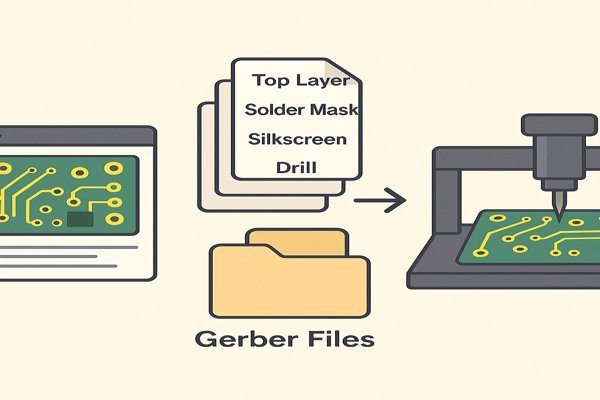
A complete Gerber package should include all necessary copper layers, solder mask layers (top and bottom), silkscreen layers (top and bottom), drill files (NC drill), and a board outline file. These files collectively define the physical and electrical specifications of your printed circuit board for the manufacturer.

Getting your Gerber files right is the cornerstone of successful PCB production. If these files aren't spot on, you could face delays, increased costs, or even a batch of unusable boards. But what exactly is their role, and how do you make sure you're generating them correctly? Let's dive into the details.
What Is the Primary Purpose of Gerber Files in the PCB Manufacturing Process?
Confused about why Gerber files are so vital in PCB fabrication? Misunderstandings here can unfortunately lead to production errors and faulty boards. They are, quite simply, the blueprint for your board.
Gerber files serve as the standard industry format for conveying detailed PCB design information to manufacturers. Each file describes a specific layer or aspect of the board, enabling automated machinery to fabricate the PCB accurately.
Unpacking the Role of Gerber Data in Production
In my experience, thinking of Gerber files as a universal language between me, the designer, and the PCB manufacturer is helpful. They were originally developed by Gerber Systems Corp (now owned by Ucamco, who continue to maintain and develop the format). The most widely used format today is RS-274X1, which embeds aperture information within the file, or the newer Gerber X2 format, which includes additional metadata. Each Gerber file typically represents a single layer of the PCB – for example, there's a file for the top copper, another for the bottom copper, one for the top solder mask, and so on. These files are essentially 2D vector images. Manufacturers feed these files into their CAM (Computer-Aided Manufacturing) systems to create the phototools or to directly image the PCB layers. This information guides the etching of copper tracks, the application of solder mask, the printing of component designators (silkscreen), and the creation of solder paste stencils. Without accurate and complete Gerbers, the physical board simply cannot be made to your specifications.
Here's a quick comparison of the common Gerber formats:
| Feature | RS-274X (Extended Gerber) | Gerber X2 (Extended Gerber with Attributes) |
|---|---|---|
| Origin | Widely adopted standard | Newer standard, builds upon RS-274X |
| Apertures | Embedded within the file | Embedded within the file |
| Metadata | Limited | Rich metadata (layer function, pad attributes, netlist info, etc.) |
| Clarity | Good, but requires clear file naming | Excellent, reduces ambiguity significantly |
| Recommendation | Still widely accepted | Preferred by Ucamco and modern manufacturers |
Using Gerber X2, when supported by your manufacturer, can prevent many common interpretation issues.
How to Make a Gerber File for PCB?
Unsure how to generate Gerbers correctly from your EDA tool? It's a common concern, as incorrect settings can lead to costly mistakes and project delays. Thankfully, the process is fairly standardized across different software.
Most PCB design software (like Altium Designer, Cadence OrCAD/Allegro, KiCad, Eagle) has a built-in export function for Gerber files. You typically select the layers you need, set the output format (RS-274X or Gerber X2 is recommended), define units, and then generate the files.
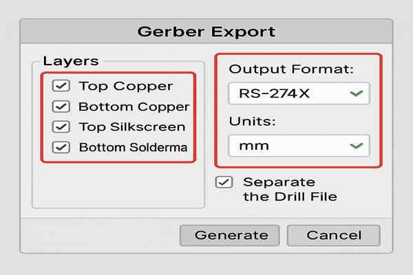
Key Steps in Generating Your Gerber Output
Generating Gerber files is a routine but critical step at the end of the PCB design phase. While the exact menu names might differ slightly between software packages, the core process is very similar. From my years using tools like Altium Designer and Cadence, I usually follow these general steps:
- Navigate to the export menu, often found under "File" > "Fabrication Outputs" > "Gerber Files" or a similar path.
- A dialog box will appear where you select all the necessary layers. This must include all copper layers, solder mask for top and bottom, silkscreen for top and bottom, paste mask for top and bottom (if SMT parts are used), and a clear board outline.
- For the format, I always choose RS-274X or, even better, Gerber X2. Avoid the obsolete RS-274-D format.
- Set the units (inches or millimeters) and precision.
- Don't forget to generate the NC Drill files2 (Excellon format typically) separately, ensuring their units and format match the Gerbers.
Here's a table summarizing key Gerber export settings:
| Setting | Recommendation | Why it Matters |
|---|---|---|
| Format | Gerber X2 (preferred) or RS-274X | X2 includes metadata, reducing errors. RS-274X is widely supported. Avoid RS-274-D. |
| Units | Match your design (Inches or Millimeters) | Consistency prevents scaling errors. |
| Precision | Inches: 2:5 (e.g., 00.00000) MM: 4:4 (e.g., 0000.0000) | Sufficient resolution for fine features. |
| Apertures | Embedded (standard for RS-274X and X2) | Eliminates need for separate aperture files. |
| Drill Files | Excellon format, match Gerber units/precision | Ensures accurate hole placement and sizing. |
Always, and I mean always, view your generated Gerber files with a separate Gerber viewer before sending them off. This final check can save a lot of headaches.
What Is the PCB Extension for Gerber Files?
Overwhelmed by the numerous file extensions your PCB software spits out? Sending the wrong set, or an incomplete set, to your manufacturer is a common pitfall that causes production headaches. Standard extensions help keep things organized.
Common Gerber file extensions include .gbr (generic), or layer-specific ones like .gtl (Gerber Top Layer), .gbl (Gerber Bottom Layer), .gts (Gerber Top Solder mask), .gbs (Gerber Bottom Solder mask), .gto (Gerber Top Overlay/Silkscreen). Drill files often use .drl or .txt.
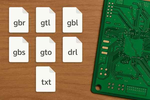
Decoding Common Gerber and Drill File Extensions
While .gbr can be used as a generic extension, and some EDA tools might use .art (artwork), using distinct extensions for each layer is a much clearer practice. This helps both you and the manufacturer quickly identify each file's purpose. The Gerber X2 format helps by embedding layer function information within the files themselves, making filenames less critical but good naming is still good practice. In my projects, I ensure my output files follow a clear naming convention. Here's a table illustrating some common extensions you'll encounter, often based on older Protel/Altium naming conventions, though these can sometimes be customized in your EDA tool:
| Layer Description | Common Extensions | Alternative Naming Example |
|---|---|---|
| Top Copper Layer | .gtl, .cmp, .g1 | ProjectName.TopLayer.gbr |
| Bottom Copper Layer | .gbl, .sol, g16 | ProjectName.BottomLayer.gbr |
| Inner Copper Layer(s) | .g2, .g3, ..., .in1 | ProjectName.Inner2.gbr |
| Top Solder Mask | .gts, .stc, .tsm | ProjectName.TopSolderMask.gbr |
| Bottom Solder Mask | .gbs, .sts, .bsm | ProjectName.BottomSolderMask.gbr |
| Top Silkscreen | .gto, .plc, .tsk | ProjectName.TopSilkscreen.gbr |
| Bottom Silkscreen | .gbo, .pls, .bsk | ProjectName.BottomSilkscreen.gbr |
| Top Paste Mask | .gtp, .ptc, .tsp | ProjectName.TopPaste.gbr |
| Bottom Paste Mask | .gbp, .pts, .bsp | ProjectName.BottomPaste.gbr |
| Board Outline | .gko, .gm1, .dim | ProjectName.BoardOutline.gbr |
| Drill Data (NC Drill) | .drl, .txt, .nc | ProjectName.NCDrill.drl |
| Drill Drawing/Map | .gd1, .drd | ProjectName.DrillDrawing.gbr |
It's crucial to provide your fabricator with a clear "read-me" file or fabrication drawing that lists all submitted files and explicitly states which layer each file represents, especially if you use custom names or if not using Gerber X2.
What Program Opens Gerber Files?
Need to check your Gerbers before sending them off but don't know how? Sending unverified design files to manufacturing is a big risk. The good news is that free and professional viewers are readily available.
Many programs can open and display Gerber files. Dedicated free viewers like Gerbv, GC-Prevue, ViewMate, or ZofzPCB are common choices. Most PCB EDA (Electronic Design Automation) tools also have an import or viewing capability for Gerbers.
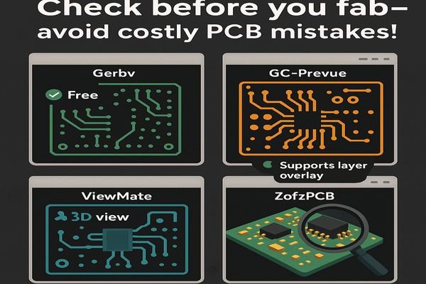
Your Toolkit for Viewing and Verifying Gerbers
You have several excellent options for viewing Gerber files, and I always make it a point to use one for a final sanity check. These tools are indispensable for ensuring your design intent is correctly translated into the manufacturing files.
Here's a breakdown of common Gerber viewer types:
| Viewer Type | Examples | Key Characteristics | My Usual Use Case |
|---|---|---|---|
| Dedicated Free Viewers | Gerbv, GC-Prevue, ViewMate (free version), ZofzPCB (3D) | Lightweight, focused on viewing & basic measurements. Some offer advanced analysis. | Quick checks, 3D visualization (ZofzPCB), cross-platform needs (Gerbv). |
| EDA Tool Built-in | Altium Designer, Cadence OrCAD/Allegro, KiCad, Eagle | Integrated with your design environment. | Comparing Gerbers against the original source design. |
| Online Viewers | Ucamco Reference Gerber Viewer, Bittele, Tracespace | No installation needed, good for quick remote checks. | Fast validation if I don't have my primary tools. |
| Professional CAM Tools | CAM350, Valor NPI, UcamX | Advanced analysis, editing, panelization capabilities. | For in-depth DFM or if I need to make minor CAM edits (rarely). |
Using a combination, like my EDA tool's viewer and a dedicated free viewer, gives me confidence before releasing files.
How Do I Read Gerber Files for PCB?
Opening Gerber files in a viewer is the first step, but truly understanding what you're looking at is key. Misinterpreting the visual data can mask critical design flaws that will only become apparent after manufacturing.
To read Gerber files, use a Gerber viewer to display the layers, either individually or stacked. You should carefully check for correct shapes, sizes, and clearances of pads and traces, and ensure proper alignment between critical layers like copper, solder mask, and drill holes.
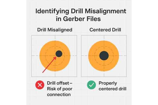
A Practical Checklist for Gerber File Inspection
"Reading" Gerber files is an active verification process. I go through a detailed checklist to ensure every aspect is correct. This has saved me from costly errors many times.
| Aspect to Check | Key Details to Verify | Common Pitfalls |
|---|---|---|
| File Completeness | All layers present: copper (all), masks (top/bottom), silkscreen (top/bottom), paste (top/bottom), outline, drill. | Missing a critical layer (e.g., bottom solder mask). |
| Layer Alignment | Solder mask openings centered on pads. Paste mask openings correct for SMT pads. Drills centered on pads/vias. | Misaligned mask causing solder bridges or exposed copper. |
| Feature Integrity | Correct pad/trace shapes and sizes. Consistent trace widths. No unintended copper shorts or opens. | Incorrect footprint dimensions, broken traces. |
| Clearances | Adequate space: trace-to-trace, trace-to-pad, pad-to-pad, copper-to-board edge. Adherence to IPC-2221B or fab specs. | Acid traps, insufficient clearance for high voltage. |
| Drill Data | All holes present, correct sizes, correct locations (plated/non-plated). No missing/extra drills. | Missing via drills, incorrect hole sizes for components. |
| Board Outline | Continuous, closed path. Correct dimensions. All internal cutouts/slots defined. | Open outline, incorrect board size for enclosure. |
| Silkscreen | Legible text. No overlap with pads/exposed copper. Correct component designators and polarity markings. | Silkscreen on pads, unreadable text. |
Using a viewer that can "flash" or toggle layers on and off helps immensely in spotting misalignments or issues.
Can I Edit a Gerber File?
Found a small error in your Gerbers after they've already been exported? The thought of going back to the EDA tool, making changes, and re-exporting everything can seem time-consuming. Minor edits directly to Gerbers might be possible.
Yes, Gerber files can be edited using specialized CAM (Computer-Aided Manufacturing) software or some advanced Gerber viewers that have editing capabilities. However, it is almost always best practice to modify the original PCB design in your EDA software and then re-export a fresh set of Gerbers.
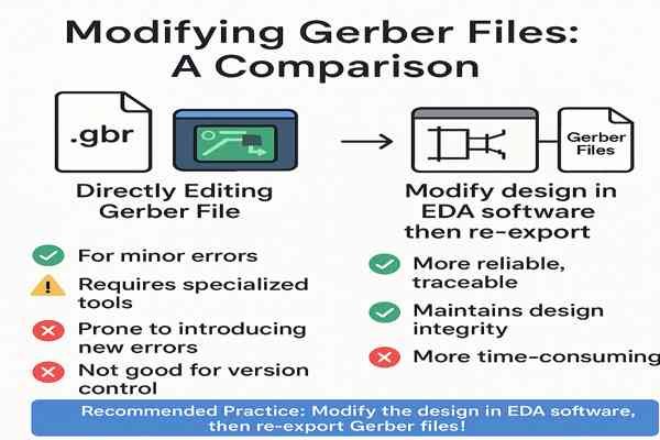
Understanding Gerber Editing: Possibilities and Pitfalls
While you can technically edit Gerber files, I treat this as a last resort. Manufacturers routinely perform CAM edits (panelization, DFM adjustments) using tools like Ucamco's UcamX or CAM350. For designers, the risks often outweigh the benefits for anything but the most trivial changes.
Here's a look at the pros and cons:
| Aspect | Pros (Limited Scenarios) | Cons (Significant Risks) |
|---|---|---|
| Speed for Minor Fixes | Potentially faster for a tiny, isolated error. | Risk of introducing new, unnoticed errors. |
| No Source Files Needed | Useful if original CAD data is lost or inaccessible. | Edited Gerbers no longer match any master design document. |
| Emergency Changes | Quick fix for a critical showstopper before immediate fab. | Creates version control nightmares; future revisions are problematic. |
| Control | Direct manipulation of manufacturing data. | Requires significant CAM expertise to avoid costly mistakes. |
My strong recommendation: always go back to your original PCB design software (Altium, KiCad, etc.), make the changes there, and then re-export. This keeps your design data consistent and reliable.
What Can You Do With Gerber Files?
Think Gerber files are only useful for sending to your PCB fabricator? Their utility actually extends much further through the product development lifecycle. You can unlock more value from these essential data files.
Gerber files are primarily used for PCB fabrication. Additionally, they are crucial for Design for Manufacturability (DFM) checks, creating solder paste stencils, generating assembly drawings and documentation, and for the archival and version control of the PCB design.
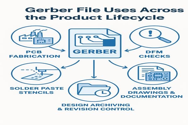
Beyond Fabrication: Diverse Applications of Gerber Data
Gerber files are the workhorse of PCB manufacturing, but their usefulness doesn't stop there. In my nearly 20 years as a hardware engineer, I've seen them leveraged for many critical tasks throughout the development cycle.
| Application | Description | Key Gerber Layers Used |
|---|---|---|
| PCB Fabrication | Core function: Defining patterns for etching, masks, silkscreen, drilling. | All layers (Copper, Mask, Silk, Paste, Drill, Outline) |
| Design for Manufacturability (DFM) Checks3 | Analyzing the design against manufacturing capabilities to identify potential production issues (e.g., track/space, annular ring). | Copper, Drill, Mask, Outline |
| Solder Paste Stencil Creation | Directly used to create stencils for applying solder paste to SMT pads. | Top and Bottom Paste Mask layers (GTP, GBP) |
| Assembly Documentation & Aids | Creating visual guides for component placement, orientation, and polarity. | Silkscreen layers (GTO, GBO), sometimes Copper and Mask layers |
| Automated Optical Inspection (AOI)4 | Used as a reference by AOI systems to inspect component placement, solder joints, and other features post-assembly. | Copper, Silkscreen, Paste |
| Test Fixture Development | Data informs the design of bed-of-nails fixtures for In-Circuit Testing (ICT) or Functional Circuit Testing (FCT). | Copper (pad locations), Drill, Netlist (from X2 or ODB++) |
| Archival & Version Control | Serves as a fixed "snapshot" of the PCB design at a particular revision for documentation, quality control, and future reference. | All layers |
Effectively utilizing Gerbers for these extended purposes can significantly improve product quality and reduce development time.
What Is the Best Gerber Editing Software?
Need to make absolutely crucial Gerber edits, perhaps for a legacy project where source files are lost, but unsure which tool to trust? Using inadequate software can corrupt your files or introduce subtle errors. Choose wisely.
For professional, reliable Gerber editing, industry-standard CAM software like Ucamco's UcamX, Siemens' Valor NPI, DownStream Technologies' CAM350, or Altium's CAMtastic (often part of Altium Designer) are the top choices. For simple viewing with very minor edits, some advanced Gerber viewers might suffice.

Choosing the Right Software for Gerber Modifications
The "best" Gerber editing software truly depends on the complexity of the editing task and who is performing it. A PCB manufacturer's CAM engineer has different needs and tools than a designer making a quick verification.
| Software Category | Examples | Typical User | Primary Use Cases |
|---|---|---|---|
| Professional CAM Suites | Ucamco UcamX, Siemens Valor NPI, DownStream CAM350 | CAM Engineers (Fab House) | Full-scale DFM checks, panelization, etch compensation, complex edits, data optimization. |
| Integrated EDA CAM Tools | Altium CAMtastic (in Altium Designer) | PCB Designers | Viewing, basic DFM, minor edits (with caution), panelization for prototypes. |
| Advanced Gerber Viewers (with some edit capability) | ViewMate Pro (paid versions) | PCB Designers, Engineers | Primarily viewing and analysis, very limited/simple edits. |
While these tools offer editing capabilities, I must reiterate my earlier advice: for designers, the safest and most robust workflow is to make all changes in the original source CAD files and regenerate the Gerbers. Direct Gerber editing should be approached with extreme caution and expertise.
How Do I Compare Gerber Files?
Unsure if your latest Gerber export perfectly matches the previous approved version, or if only the intended changes were made? Sending inconsistent or incorrect files to your fab house leads to chaos and costly rework. Comparison tools are designed to prevent this.
Gerber comparison is performed using specialized software that graphically and logically analyzes two sets of Gerber files, layer by layer, highlighting any differences. Many CAM tools (like CAM350, Valor NPI) and some advanced Gerber viewers offer this critical functionality.
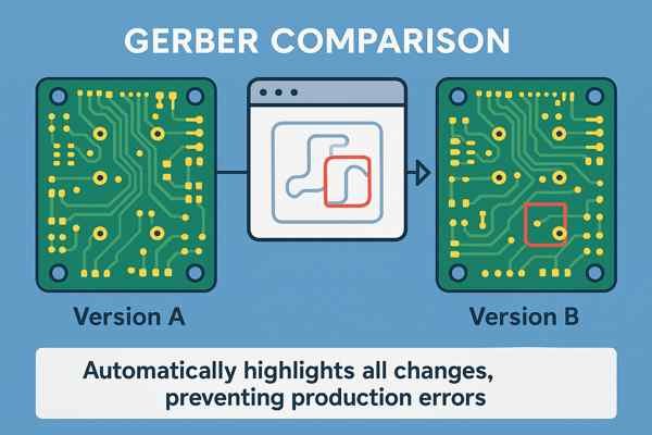
Ensuring Accuracy: The Gerber Comparison Process
Comparing Gerber files is a vital quality assurance step, especially when I'm managing PCB revisions. It's the best way to ensure that only the intended modifications have made it into the manufacturing data.
| Reason for Comparison | Why It's Critical | Tools Offering This Feature |
|---|---|---|
| Verify Design Revisions | Confirms that only documented changes between versions (e.g., Rev A to Rev B) are present. | CAM350, Valor NPI, Altium Designer, various dedicated diff tools. |
| Ensure Data Export Integrity | Checks that the EDA tool's export process didn't introduce errors or unintended artifacts. | Most CAM tools, some advanced Gerber viewers. |
| Validate Supplier Changes | If a manufacturer makes agreed-upon DFM adjustments, comparison verifies their accuracy. | Professional CAM software. |
| Prevent Accidental Changes | Catches any unintentional modifications before files are sent to fabrication. | Any reliable Gerber comparison tool. |
The comparison process typically involves a graphical "XOR" or similar image analysis between two corresponding layers. Differences are visually highlighted, making it easy to spot discrepancies. Before sending any revised design for fabrication, I always run a Gerber compare against the previously manufactured version. This simple step has caught subtle issues that could have led to expensive mistakes.
What Is the Alternative to Gerber Files?
Tired of juggling a folder full of individual Gerber files for every single PCB design? A more integrated, intelligent file format could simplify your workflow and reduce the risk of errors. Alternatives to the traditional Gerber-plus-drill-file package do exist.
The main, well-established alternative to Gerber files is ODB++. Another intelligent format, which is open and gaining traction, is IPC-2581. Both these formats offer a more holistic data structure, bundling multiple types of design information into a single file or package, unlike the layer-by-layer approach of Gerber.
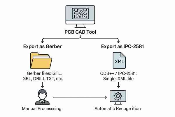
Exploring Modern Alternatives to Traditional Gerbers
While Gerber (especially X2) remains dominant, these intelligent formats offer a more streamlined and less error-prone approach by consolidating data.
| Feature | Gerber (RS-274X / X2) | ODB++ (Open DataBase++) | IPC-25815 |
|---|---|---|---|
| Data Structure | Multiple individual files per layer/function | Single hierarchical file/directory structure | Single XML-based file |
| Content | Primarily graphical layer data; X2 adds some metadata. | Layers, drill, netlist, components, stack-up, sometimes BOM. | Layers, stack-up, materials, netlist, BOM, assembly data. |
| Intelligence | Limited (X2 improves this) | High (designed as an intelligent database) | High (designed for comprehensive data exchange) |
| Risk of Error | Higher (missing files, misinterpretation of layers) | Lower (all data is integrated) | Lower (all data is integrated) |
| Adoption | Universal | Widely adopted, especially for complex designs; proprietary roots but open. | Growing adoption, open standard |
| My Take | Reliable workhorse, X2 is a good step forward. | Excellent for complex boards, reduces ambiguity with fabs. | Promising open standard, gaining momentum. |
For my complex projects, especially those involving HDI or critical impedance control, I often prefer to supply ODB++ if the manufacturer is well-equipped for it, as it bundles crucial stack-up and netlist information, reducing potential communication errors.
What Is an ODB++ File?
You might have heard the term ODB++ mentioned, especially by PCB manufacturers or in discussions about advanced EDA tools, but what exactly is it and what makes it different from the familiar Gerber files?
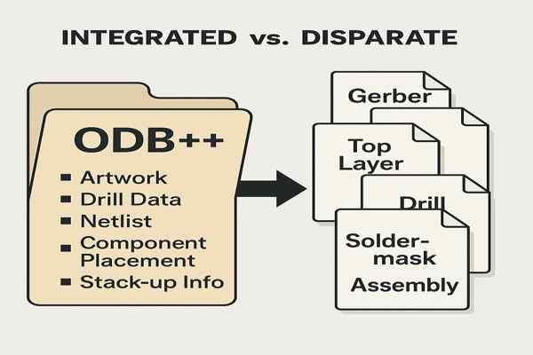
ODB++ is an intelligent, all-in-one CAD-to-CAM data exchange format for printed circuit boards. It consolidates PCB layer artwork, drill data, netlist information, component placement details, and layer stack-up specifications into a single, structured database or file archive.
A Closer Look at the ODB++6 Data Structure
ODB++ stands for Open DataBase, with the "++" signifying its enhanced capabilities. It was originally created by Valor Computerized Systems (now Siemens). Its core strength is packaging all necessary manufacturing data into a single, coherent structure, usually a compressed archive like .tgz or .zip.
An ODB++ dataset typically contains the following key components:
| ODB++ Component | Description | Importance |
|---|---|---|
| Matrix | Defines layers, their order, type (signal, power, mask, etc.), materials, and overall board stack-up. | Critical for correct layer construction and impedance control. |
| Layer Files | Contains the graphical data (artwork) for each physical layer, with more context than individual Gerbers. | Defines the conductive patterns, solder mask openings, etc. |
| Netlist Data | Describes electrical connectivity (nets), component pins, and test points. | Essential for bare-board electrical testing (flying probe, bed-of-nails). |
| Component Information | Can include component outlines, pin locations, rotation, polarity, and sometimes BOM attributes. | Vital for automated assembly (pick-and-place) and inspection. |
| Drill and Rout Data | All information for drilling, milling, scoring, and other mechanical operations. | Ensures accurate hole placement, board outline, and cutouts. |
| EDA Data (Optional) | Can include original CAD net names, padstack information, etc. | Provides richer context for CAM engineers and DFM analysis. |
Using ODB++ has, in my experience, significantly streamlined communication with manufacturers for complex boards. It reduces the back-and-forth about missing files or unclear stack-up details, leading to faster CAM processing and fewer errors.
Conclusion
Ensuring you provide a complete and accurate Gerber set, or use a modern integrated format like ODB++, is absolutely fundamental for PCB manufacturing success. Always double-check your exports; it saves immense time and money.
-
Learn about RS-274X, its features, and how it stands against newer formats like Gerber X2 for effective PCB design. ↩
-
Understanding NC Drill files is crucial for accurate hole placement in PCB designs, ensuring quality manufacturing. ↩
-
Understanding DFM checks can enhance your PCB design process, ensuring manufacturability and reducing production issues. ↩
-
Exploring AOI can help you understand how to ensure quality in PCB assembly, reducing defects and improving reliability. ↩
-
Learn how IPC-2581 facilitates comprehensive data exchange in PCB manufacturing, making it a promising open standard. ↩
-
Exploring this resource will provide a deeper understanding of ODB++ and its role in PCB design and manufacturing. ↩


