 Skip to content
Struggling to kickstart your PCB design? Unsure what information is crucial before you even open your EDA software? Getting this right upfront saves massive headaches later.
To design a Printed Circuit Board (PCB), you fundamentally need a schematic diagram, a Bill of Materials (BOM), and mechanical constraints. These inputs define the circuit's logic, the components used, and the physical shape and limitations of the board.

Getting the initial inputs correct for your PCB design is like laying a strong foundation for a house. If you miss something critical at this stage, the entire project can become wobbly, leading to frustrating revisions, blown budgets, and missed deadlines. I've seen it happen too many times. So, let's break down what you absolutely need to gather before you start, ensuring your design journey is smooth and successful. We'll explore each key input in more detail.
What Do You Need To Build A PCB?
Wondering what it takes to turn a design into a physical board? It's more than just a good idea. You need precise manufacturing files.
To build a PCB, manufacturers require Gerber files (for copper layers, solder mask, silkscreen), an NC drill file (for holes), a BOM (for component purchasing), and often assembly drawings and pick-and-place data (for automated assembly).
Essential Files for PCB Fabrication and Assembly
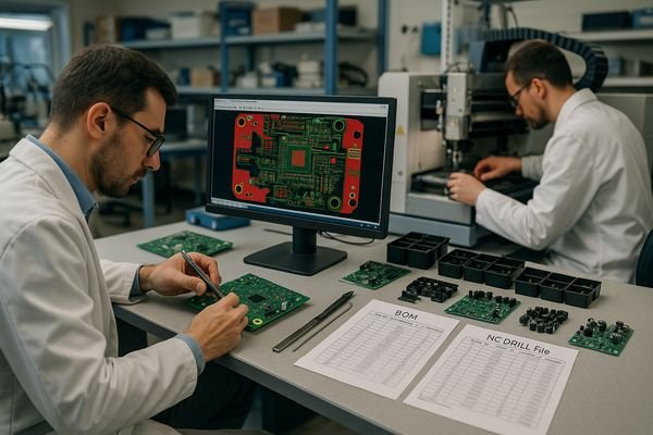
When I talk about building a PCB, I mean the actual fabrication (making the bare board) and assembly (placing components on it). This process requires a specific set of data files that you, as the designer, provide to the manufacturer. Without these, they can't accurately translate your design into a physical product.
The primary files are often grouped into fabrication data and assembly data.
| File Type | Purpose | Common Format(s) | Notes |
|---|---|---|---|
| Gerber Files1 | Defines copper layers, solder mask, silkscreen, paste mask, board outline | RS-274X (Extended Gerber) | One file per layer. Ucamco is the definitive source for Gerber format. |
| NC Drill File | Specifies location and size of all drilled holes (vias, mounting holes) | Excellon, Sieb & Meyer | Essential for creating interconnections between layers and mounting. |
| Bill of Materials (BOM)2 | Lists all components, quantities, reference designators, part numbers | .xls, .csv, .txt | Crucial for component procurement and placement. |
| Pick and Place Data3 | Provides X-Y coordinates and rotation for each component for automated assembly | .txt, .csv | Also known as Centroid data. Essential for SMT assembly. |
| Assembly Drawing(s) | Visual guide for component placement, orientation, special instructions | PDF, Gerber | Especially important for manual assembly or complex parts. |
| Netlist (optional) | Describes electrical connectivity; used for bare-board testing (ICT/Flying Probe) | IPC-D-356 | Helps verify no shorts or opens on the fabricated board. |
I remember a project early in my career where we sent an incomplete Gerber set. The manufacturer assumed a missing layer was intentional, and the first batch of prototype boards was completely useless. That mistake cost us a week and a few thousand dollars. So, always double-check your manufacturing package before sending it out. A good practice is to use a Gerber viewer to inspect all layers yourself.
How To Design A PCB Step By Step?
Feeling overwhelmed by the PCB design process? Knowing the steps can make it manageable. A structured approach prevents errors and saves time.
PCB design involves: 1. Schematic capture, 2. Component footprint creation/selection, 3. Board outline and mechanical definition, 4. Component placement, 5. Routing, 6. Design Rule Check (DRC), and 7. Gerber/manufacturing file generation.
A Phased Approach to PCB Design: From Concept to Manufacturing Files
Designing a PCB is a systematic engineering task. It's not just art; it's applying rules and best practices to create a functional electronic circuit on a physical board. I always follow a clear workflow.
Phase 1: Conceptualization and Logical Design
This phase is about defining what the circuit does and how it's interconnected.
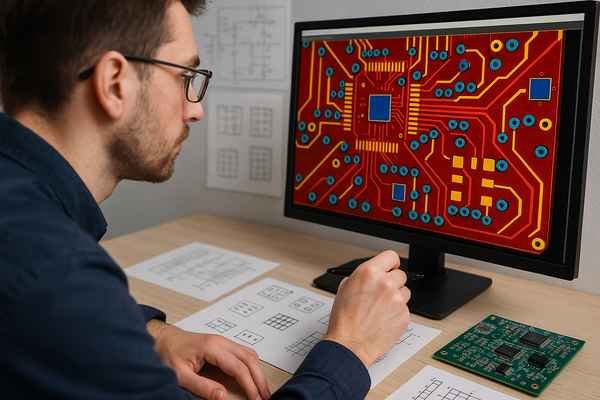
- Schematic Capture: This is the starting point. You use an EDA (Electronic Design Automation) tool like Altium Designer, Cadence OrCAD/Allegro, or KiCad to draw the circuit diagram. This involves placing symbols for each component (resistors, capacitors, ICs, connectors) and drawing wires (nets) to connect them.
- Component Selection & Footprint Association: For every component in your schematic, you need to choose a real-world part and assign its corresponding physical footprint. Footprints define the copper pad patterns on the PCB where the component will be soldered. Many EDA tools have libraries, but you often need to create or verify custom footprints based on manufacturer datasheets. The IPC-73514 standard is a valuable resource for footprint design guidelines.
Phase 2: Physical Layout
Here, you translate the schematic into a physical board design.
| Step | Key Activities | Important Considerations |
|---|---|---|
| Board Outline & Stack-up | Define the physical board shape, size, mounting holes. Define the layer stack-up (number of layers, materials, thicknesses). | Mechanical constraints from enclosure, impedance control requirements for high-speed signals. |
| Component Placement | Arrange components on the board. | Signal flow, thermal management, minimizing trace lengths, accessibility for testing. |
| Routing | Draw copper traces to connect components according to the schematic netlist. | Signal integrity, power integrity, trace widths for current, clearances, via usage. |
Phase 3: Verification and Output Generation
Before manufacturing, thorough checks are essential.
- Design Rule Check (DRC)5: The EDA tool checks your layout against predefined rules (e.g., minimum trace width, spacing between traces and pads). These rules often come from your PCB manufacturer's capabilities. For example, a typical minimum trace/space might be 5 mils (0.127 mm), but this can vary.
- Cross-Probing and Netlist Verification: Ensure the layout accurately reflects the schematic.
- Manufacturing File Generation: Create the Gerber files, NC drill file, BOM, and other necessary outputs discussed earlier.
I once rushed the DRC on a complex board to meet a tight deadline. The result? A batch of boards with a critical short between a power plane and ground. That lesson taught me that spending an extra hour on DRC can save days of debugging and thousands in costs.
What Is The 3W Rule In PCB Design?
Ever had issues with crosstalk on your PCB? The 3W rule is a simple guideline to help minimize this. It's easy to remember and apply.
The 3W rule states that the distance between the centerlines of two adjacent traces should be at least three times the width of a single trace. This helps minimize electromagnetic interference (EMI) and crosstalk between signals.
Applying the 3W Rule: Understanding Spacing for Crosstalk Reduction
Crosstalk is a common headache in PCB design, especially with faster signals. It's the unwanted coupling of signals between adjacent traces. The 3W rule is a widely cited heuristic to mitigate this.
Understanding the 'W'
The 'W' in the 3W rule refers to the width of your signal traces. The rule essentially dictates the minimum spacing needed to reduce the electromagnetic fields from one trace interfering with another.
Practical Application and Benefits
Let's break it down with an example:
| Trace Width (W) | Min. Centerline-to-Centerline Spacing (3W) | Min. Air Gap (Edge-to-Edge Spacing, 2W) |
|---|---|---|
| 5 mils (0.127mm) | 15 mils (0.381mm) | 10 mils (0.254mm) |
| 8 mils (0.203mm) | 24 mils (0.610mm) | 16 mils (0.406mm) |
| 10 mils (0.254mm) | 30 mils (0.762mm) | 20 mils (0.508mm) |
According to industry literature, such as "Signal Integrity for High-Speed Digital Designs" by Thierauf, applying the 3W rule can reduce crosstalk6 by approximately 70% compared to minimum spacing. For even better isolation (around 98%), a 10W spacing might be considered for highly sensitive or aggressive signals. However, 3W is a good starting point for most digital signals. Remember, it's a guideline, not an absolute law. For critical nets, especially at high frequencies (e.g., >100 MHz), you should perform signal integrity simulations to verify performance rather than relying solely on rules of thumb. I always apply it to clock lines and data buses as a first pass.
What Are The Main Components Of A PCB?
New to electronics and wondering what makes up a PCB? It's not just the green board; there are key elements that give it structure and function.
The main components of a PCB are the substrate (the base material, often FR-4), copper layers (for traces and planes), solder mask (protective coating), and silkscreen (for component labels and markings).
Deconstructing the Board: Core and Protective PCB Layers
A Printed Circuit Board might look simple from the outside, but it's a layered structure where each layer has a specific purpose. These layers combine to provide both the physical support and electrical connectivity for your electronic components.
Core Structure of a PCB
These are the fundamental parts that make up the board itself.
| PCB Element | Typical Material(s) | Primary Function | Common Specifications |
|---|---|---|---|
| Substrate | FR-47 (woven glass & epoxy), Polyimide (flex), Rogers materials (RF) | Provides mechanical support and electrical insulation between copper layers. | Thickness (e.g., 1.6mm, 0.8mm) |
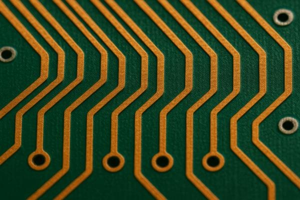
| Copper Foil | Copper (Cu) | Forms conductive traces, pads, and planes for electrical signals and power. | Thickness (e.g., 0.5oz, 1oz, 2oz) |
The substrate is the backbone. FR-4 is the workhorse for most rigid PCBs due to its good balance of cost, durability, and electrical properties. Its dielectric constant is typically around 4.2 to 4.7. Copper thickness is often specified in ounces per square foot (e.g., 1 oz copper is about 35 µm or 1.37 mils thick).
Protective and Informative Layers
These layers are applied on top of the copper and substrate.
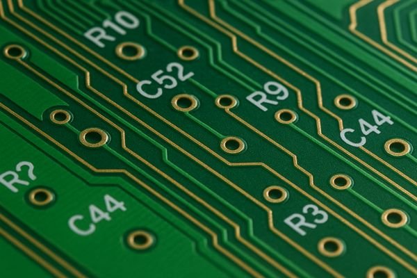
- Solder Mask8: This is a polymer coating (often green, but can be blue, red, black, etc.) applied over the copper traces. Its main jobs are to protect the copper from oxidation and to prevent solder bridges from forming between closely spaced pads during the soldering process. Openings in the solder mask expose the pads where components will be soldered.
- Silkscreen9: Applied on top of the solder mask, this layer uses non-conductive ink to print text and graphics, such as component reference designators (R1, C1, U1), component outlines, polarity marks, company logos, and other identifying information. This greatly aids in assembly, testing, and debugging. I always make sure my silkscreen text is legible and doesn't overlap solder pads.
Understanding these basic components helps in making informed decisions during the design process, like selecting appropriate materials for your application's needs.
What Mechanical Constraints Affect PCB Design?
Think PCB design is just about connecting dots? Mechanical factors often dictate your board's shape, size, and even component choices. Ignoring them is risky.
Mechanical constraints include board dimensions and shape, mounting hole locations, connector positions and types, component height restrictions, keep-out areas, and considerations for enclosures or mating parts. These are critical for a functional fit.
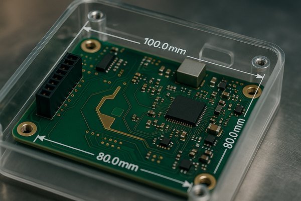
Mechanical constraints are some of the first pieces of information I seek when starting a new PCB design. These define the physical world your board must live in. Getting these wrong means your beautifully designed PCB might not fit into its enclosure or connect to other parts of the system.
Board-Level Constraints
These relate to the overall physical characteristics of the PCB itself.
| Constraint Type | Description | Impact on Design |
|---|---|---|
| Board Outline/Size | The precise physical dimensions (length, width) and shape of the PCB. | Dictates available area for component placement and routing. |
| Mounting Holes | Location, diameter, and type (e.g., plated/non-plated) of holes for securing the PCB. | Restricts component placement in these areas; critical for secure assembly. |
| Connector Placement | Fixed locations for connectors to interface with external cables or other boards. | Often a primary driver for overall component layout and signal routing paths. |
| Keep-Out Areas | Regions where no components, traces, or vias are allowed. | Due to other mechanical parts, high voltage, RF shielding, etc. |
Component-Level and System Constraints
These relate to the components themselves and how the PCB interacts with its surroundings.
- Component Height Restrictions: Maximum allowable height for components in certain areas or across the entire board, dictated by the enclosure or adjacent parts. This can limit your choice of capacitors, connectors, or heat sinks. For example, a slim product might allow a maximum component height of only 2mm.
- Material & Thickness: Sometimes, specific PCB materials or overall thickness are dictated by mechanical strength requirements or specific impedance needs that interact with mechanical design.
- Enclosure Fit: How the PCB fits within its housing. This includes clearances to enclosure walls, alignment of LEDs or sensors with openings, and ensuring no interference. I always request a 3D model of the enclosure if available. It saved me on a project where a tall capacitor was just millimeters from shorting against a metal casing in the initial design. Catching that in the 3D model review prevented a costly board respin.
How Long Does It Take To Design A PCB?
"How long will this take?" – the classic project question. For PCBs, it's not a one-size-fits-all answer. Complexity is the main driver.
PCB design time varies greatly: a simple 2-layer board might take a few days to a week. A moderately complex 4-6 layer board could take 2-4 weeks. A highly complex board with high-speed interfaces or many components can take 1-3+ months.

Estimating Your Timeline: PCB Design Duration by Complexity
Estimating PCB design time is crucial for project planning. It's not an exact science, as unforeseen issues can always arise, but experience provides good general guidelines.
Factors Influencing Design Time
Several key factors determine how long a PCB design will take:
- Complexity: Number of components, signal types (digital, analog, RF, high-speed), density of placement.
- Number of Layers: More layers generally mean more complex routing and stack-up considerations.
- Technology Used: High-speed interfaces (DDR memory, PCIe, USB 3.0), fine-pitch BGAs, HDI (High-Density Interconnect) technology significantly increase design effort.
- Engineer's Experience: A seasoned designer will typically be faster and more adept at foreseeing problems.
- Tool Proficiency: Familiarity with the EDA software.
- Clarity of Inputs: Well-defined schematics and mechanicals save time. Ambiguity leads to delays.
Typical Timeframes by Complexity
These are rough estimates for the actual design work (schematic review, layout, routing, DRC, Gerber generation) for a single engineer. This doesn't include schematic creation from scratch, firmware development, or multiple major revisions.
| Board Complexity | Typical Layers | Approx. Component Count | Estimated Design Hours | Estimated Calendar Time |
|---|---|---|---|---|
| Simple | 2 (rarely 4) | < 100 | 20 - 60 hours | 3 days - 1.5 weeks |
| Moderately Complex | 4 - 8 | 100 - 500 | 80 - 200 hours | 2 - 5 weeks |
| Highly Complex | 8 - 16+ | 500 - 2000+ | 200 - 500+ hours | 1 - 3+ months |
For instance, a basic Arduino-style shield (simple) might be on the lower end. A motherboard for a computer (highly complex) would be at the high end or even exceed these estimates, often involving a team. I once worked on a 12-layer board with multiple FPGAs and DDR3 memory; the layout phase alone took two senior engineers nearly two months. Always buffer your estimates!
How Much Does It Cost To Have Someone Design A PCB?
Need a PCB designed but not sure about the budget? Costs can vary widely. Knowing the influencing factors helps in getting realistic quotes.
Hiring a PCB designer can cost from $50 to $200+ per hour. A simple board might cost $500-$2,000. Moderately complex boards: $2,000-$10,000. Highly complex boards can exceed $10,000-$20,000+, depending on expertise and project scope.

Budgeting for Expertise: Understanding PCB Design Service Costs
The cost of PCB design services can seem opaque, but it generally correlates with the time and expertise required.
Cost Models
- Hourly Rate: Most common for freelance designers and design houses. Rates vary by experience, location, and specialization.
- Basic Layout (e.g., less critical boards, some overseas freelancers): $40 - $75 per hour
- Experienced Designers / Standard Complexity (e.g., many US/EU freelancers, smaller firms): $75 - $150 per hour
- Specialized/High-Complexity (e.g., RF, high-speed, medical, large design firms): $125 - $250+ per hour
- Fixed Project Price: Some designers or firms offer a fixed price, especially for well-defined, simpler projects. This is less common for complex or R&D-heavy designs where scope creep is likely.
Factors Determining Final Cost
Beyond hourly rates, these elements influence the total project cost:
| Factor | Impact on Cost | Example |
|---|---|---|
| Board Complexity | (As defined in "Estimating Your Timeline" section) Higher complexity = higher cost. | A 12-layer DDR4 memory board will cost vastly more than a 2-layer LED flasher. |
| Technology Requirements | Specialized needs like controlled impedance, RF, HDI, via-in-pad. | Designs needing signal integrity analysis or specific high-frequency materials increase cost. |
| Deliverables | Basic Gerbers vs. full documentation package (assembly drawings, 3D models, test plans). | More comprehensive deliverables require more engineering time. |
| Number of Revisions | Unforeseen changes or multiple iterations. | It's wise to budget for at least one minor revision cycle. |
| Turnaround Time | Rush jobs often incur premium charges. | If you need a board designed in half the normal time, expect to pay more. |
To give a very rough idea using the timeframes from the previous section and a blended rate of, say, $100/hour:
- Simple Board: 20-60 hours -> $2,000 - $6,000 (though some services offer simpler designs for $500-$1,500)
- Moderately Complex Board: 80-200 hours -> $8,000 - $20,000
- Highly Complex Board: 200-500+ hours -> $20,000 - $50,000+
I always advise getting multiple quotes and clearly defining the scope of work to avoid surprises. Remember, investing in good design upfront often saves much more on manufacturing issues and product failures later.
What Are Common Mistakes To Avoid In PCB Design?
Want your PCB to work on the first try? Avoiding common pitfalls is key. Learning from others' mistakes saves you time and money.
Common mistakes include: incorrect footprints, insufficient power/ground planes or trace widths, violating DRCs, poor component placement leading to EMI or thermal issues, and not considering DFM (Design for Manufacturability).
Sidestepping Pitfalls: Common Errors in PCB Design and How to Prevent Them
In my nearly 20 years of hardware engineering, I've seen many PCB designs – some great, some less so. Certain mistakes tend to reappear, causing costly respins and delays. Awareness is the first step to avoidance.
Footprint and Library Errors
These are insidious because the schematic might be perfect, but the physical board will be wrong.
- Incorrect Footprints: Using a footprint that doesn't match the physical component dimensions. This is a classic.
- Consequence: Components can't be soldered, or are soldered incorrectly.
- Prevention: Always verify footprints against manufacturer datasheets. Create and meticulously check your own library parts for custom components. Many companies have a dedicated librarian role for this reason. IPC-7351B10 is a good standard for footprint guidelines.
- Pin Mapping Errors: Schematic symbol pins not matching the footprint pads correctly (e.g., pin 1 on symbol is pad 3 on footprint).
- Consequence: Circuit malfunction, damaged components.
- Prevention: Rigorous library part creation process, peer review of new symbols/footprints.
Electrical Rule and Signal Integrity Violations
| Mistake Category | Common Examples | Potential Consequences | Prevention Strategies |
|---|---|---|---|
| Power Delivery Network (PDN) | Insufficient trace widths for current, inadequate decoupling capacitors, poor ground plane design. | Voltage drops, noise, unstable operation, overheating. | Use trace width calculators (e.g., IPC-2152 standard for guidance). Place decoupling caps close to IC power pins. Aim for solid ground planes. |
| Signal Integrity (SI) | Lack of impedance control for high-speed traces, stubs on critical nets, excessive vias, crosstalk. | Data errors, EMI radiation, reflections, timing issues. | Follow high-speed design rules (e.g., differential pair routing, length matching). Use SI simulation tools for critical nets. |
| Ignoring Design Rule Checks (DRC) | Not running DRC, or using incorrect rule sets from the manufacturer. | Shorts, opens, spacing violations, manufacturability issues. | Always run DRC with manufacturer-supplied rules. Address every violation. |
Manufacturability and Assembly Oversights
- Poor Component Placement: Components too close together for assembly machines, blocking test points, or creating thermal hotspots.
- Consequence: Assembly difficulties, increased cost, overheating, reduced reliability.
- Prevention: Follow DFM guidelines (Design for Manufacturability11), consider thermal airflow, ensure test point accessibility. Many assemblers provide DFM guidelines; for example, minimum component spacing might be 0.5mm.
- Via Mismanagement: Vias in pads (unless specifically designed as via-in-pad plated over), vias too close to pads causing solder wicking.
- Consequence: Tombstoning of components, poor solder joints, open circuits.
- Prevention: Adhere to manufacturer guidelines on via placement relative to pads.
One time, a junior engineer on my team designed a board where a tiny surface-mount resistor was placed directly under a large electrolytic capacitor. It was impossible to inspect or rework the resistor once the capacitor was placed. A simple DFM check would have caught that. Learning from these common errors can significantly improve your first-pass success rate.
Conclusion
In essence, successful PCB design hinges on thorough preparation: clear schematics, an accurate BOM, and well-defined mechanicals. These inputs are your roadmap.
-
Understanding Gerber Files is crucial for ensuring accurate PCB manufacturing. Explore this link to learn more about their importance and usage. ↩
-
A comprehensive BOM is vital for successful PCB assembly. Discover more about its components and how to create one effectively. ↩
-
Pick and Place Data is essential for automated assembly processes. Learn how it streamlines production and improves accuracy. ↩
-
Explore the IPC-7351 standard to enhance your PCB footprint design skills and ensure compliance with industry best practices. ↩
-
Understanding DRC is crucial for ensuring your PCB layout meets manufacturing standards and avoids costly errors. ↩
-
Exploring methods to reduce crosstalk can enhance your PCB designs, ensuring better performance and reliability in high-speed applications. ↩
-
Explore this link to understand why FR-4 is the go-to material for most rigid PCBs, balancing cost and performance effectively. ↩
-
Learn about the critical role of solder masks in protecting PCBs and ensuring reliable soldering processes. ↩
-
Discover how silkscreen printing enhances PCB usability and aids in the assembly process, making it essential for effective design. ↩
-
Explore IPC-7351B to understand footprint guidelines that can prevent costly PCB design errors. ↩
-
Learn about DFM best practices to enhance assembly efficiency and reduce costs in PCB production. ↩


