 Skip to content
Are you struggling with mysterious noise issues in your mixed-signal designs? You’ve separated your analog and digital sections, but sensitive signals are still getting corrupted. The culprit might be hiding in your power delivery network.
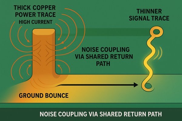
The primary way high currents in heavy copper traces create noise is through magnetic field coupling and, more critically, by causing voltage drops along the shared return path. This fluctuating return path voltage, often called "ground bounce," directly injects noise into signal traces that use the same plane as a reference.
This article dives into the subtle ways power and signal integrity interact on a heavy copper PCB. I’ll share what I've learned from nearly two decades of hardware engineering, moving beyond the obvious to uncover the root causes of noise. We’ll explore how to design robust PCBs where high-power and sensitive signals can coexist peacefully, ensuring your products are reliable and pass EMI testing.
How Do Signals and Power Coexist on a Heavy Copper PCB?
Having trouble keeping your power circuits from interfering with your sensitive analog signals? It feels like a constant battle between delivering clean power and maintaining signal integrity, especially on a dense board.
To have signals and power coexist, you must physically partition your layout, use dedicated ground and power planes, and meticulously manage the return paths. High-current paths should be short and wide, while sensitive signal traces are routed away from these noisy areas, using the ground plane as a shield.
Strategic Partitioning and Return Path Control
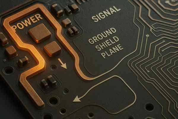
Effective coexistence isn't about one magic trick; it's about a disciplined design approach. The first step is physical and thermal partitioning. On your board, create distinct regions for high-power switching circuits, digital logic, and sensitive analog circuits. Just as importantly, keep hot-running power components away from temperature-sensitive analog ICs.
The core of this strategy is managing the return currents. At low frequencies (and for DC), current takes the path of least resistance. At high frequencies, like the fast-switching edges in a power supply, the return current takes the path of least impedance, which is directly underneath the trace in the reference plane to minimize loop area. My experience on projects at Honeywell taught me that if you disrupt this high-frequency return path—for example, by forcing it to go around a slot or a different ground area—you create a large current loop. A large loop is an efficient antenna that radiates noise and can corrupt adjacent signals. Imagine the high-frequency return current as a shadow cast directly beneath the trace; your job is to ensure nothing ever blocks or distorts that shadow.
| Strategy | Principle | Implementation Detail |
|---|---|---|
| Functional Partitioning | Keep noisy circuits away from quiet ones. | Dedicate separate areas of the PCB for power, digital, and analog sections. Enforce strict "keep-out" zones. |
| Layer Stack-up | Use planes to shield and provide a return path. | Place a solid ground plane between a high-current layer and a signal layer. |
| Return Path Routing | Minimize loop areas for high-frequency currents. | Route power traces and their returns as close together as possible, ideally on adjacent layers. |
| Thermal Partitioning | Prevent heat from affecting sensitive parts. | Position high-power components away from analog ICs or use thermal vias to draw heat away. |
How Does Localized Heat From Power Traces Affect Signal Impedance?
Are your high-speed signals failing, even though your layout looks perfect? You may have accounted for trace width and dielectric spacing, but the heat from a nearby heavy copper trace could be silently sabotaging your impedance control.
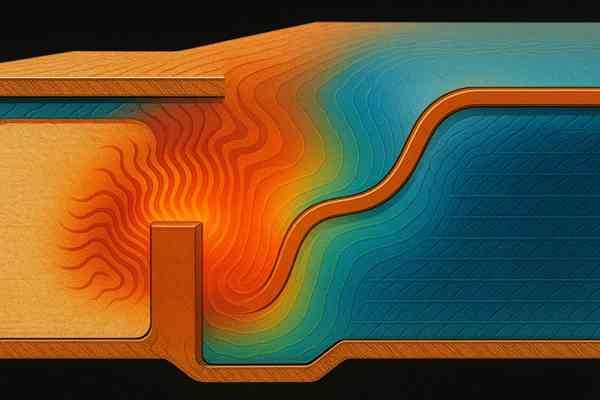
Localized heat from a power trace raises the temperature of the adjacent dielectric material. This changes the material's dielectric constant (\(D_{k}\)), which in turn alters the characteristic impedance of nearby signal traces. For typical FR-4, this can cause impedance shifts that disrupt signal integrity.
Understanding the Thermal-Impedance Link
The characteristic impedance (\(Z_{0}\)) of a trace is a function of its geometry and the dielectric constant (\(D_{k}\)) of the material surrounding it. The problem is that \(D_{k}\) is not a fixed number; it varies with temperature. For standard FR-4, the thermal coefficient of the dielectric constant can cause \(D_{k}\) to decrease as temperature rises.
Let’s think about what this means. A high-current trace can easily heat up by 20°C to 40°C above ambient. This heat spreads to the surrounding FR-4. As the \(D_{k}\) of the dielectric under your signal trace decreases, its impedance will increase. A controlled 50 \(\Omega\) trace might drift up to 52 or 53 \(\Omega\). While this seems small, for a high-speed interface like DDR memory, this mismatch can cause signal reflections, increasing bit error rates and causing system failures. For differential pairs, a temperature gradient across the two traces can introduce skew, converting common-mode noise into damaging differential-mode noise.
| Material Property | Relationship with Temperature | Impact on Impedance (\(Z_{0}\)) |
|---|---|---|
| Dielectric Constant (\(D_{k}\))1 | Decreases as temperature increases. | \(Z_{0} \propto \frac{1}{\sqrt{D_{k}}}\), so impedance increases. |
| Copper Resistivity | Increases as temperature increases. | Increases \(I \times R\) losses, contributing more heat. |
| Differential Skew | Caused by temperature gradients. | Degrades differential signaling performance. |
To mitigate this, you can increase spacing, add thermal vias, or choose a more stable dielectric material.
| PCB Material | Typical \(D_{k}\) (@ 1GHz) | Thermal Coefficient of \(D_{k}\) (ppm/°C) | Thermal Conductivity (W/m·K) |
|---|---|---|---|
| Standard FR-4 | 4.3 – 4.7 | -200 to -300 | 0.25 |
| Rogers RO4350B | 3.48 | +40 | 0.69 |
| IMS (Aluminum) | N/A (thin dielectric) | Varies | 1.0 – 3.0 |
As shown, Rogers materials are far more stable with temperature but cost more. Insulated Metal Substrates (IMS) offer the best thermal dissipation for power-heavy designs.
What Is an Optimal Layer Stack-up for Isolating Power and Signal Layers?
Are you unsure how to arrange your PCB layers? A poor stack-up can force power noise onto your signal layers, creating EMI and signal integrity nightmares that are impossible to fix after fabrication.
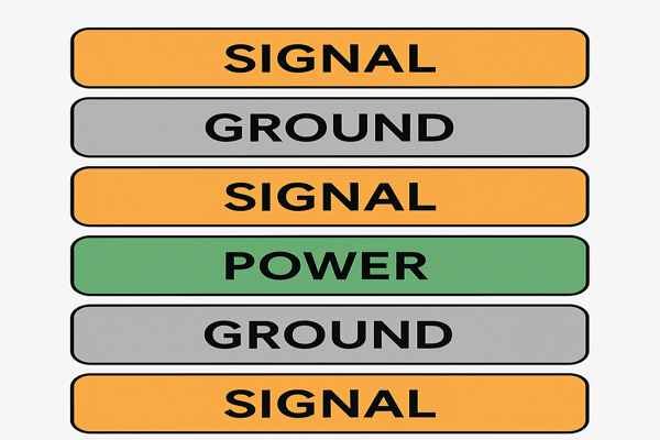
An optimal stack-up for isolation places a solid ground plane between a high-current power layer and any sensitive signal layers. For a multi-layer board, a common high-performance stack-up is: Signal | Ground | Signal | Power | Ground | Signal. This provides excellent shielding and controlled return paths.
Designing a High-Isolation PCB Stack-up
Your layer stack-up is the foundation of your board's performance. A key principle is creating plane capacitance. By placing a power and ground plane very close together (e.g., 3-5 mils), you create a large, parallel-plate capacitor embedded within the PCB itself. This provides an extremely low-inductance decoupling path that is effective at very high frequencies.
For a high-current, mixed-signal design, an 8-layer stack-up offers great isolation. Here is a recommended configuration:
| Layer # | Layer Name | Copper Weight | Primary Purpose |
|---|---|---|---|
| 1 | Top Signal | 1 oz | Components and low-speed signals. |
| 2 | Ground Plane | 1 oz | Solid ground, reference for L1. |
| 3 | High-Speed Signal | 0.5 oz | Stripline routing, shielded by L2 and L4. |
| 4 | Power Plane | 2-4 oz | Heavy copper for main power delivery. |
| 5 | Ground Plane | 1 oz | Tightly coupled to L4 for plane capacitance and shielding. |
| 6 | High-Speed Signal | 0.5 oz | Alternative stripline layer, reference to L5. |
| 7 | Power Plane | 1 oz | Low-current analog or secondary digital rails. |
| 8 | Bottom Signal | 1 oz | Components and non-critical signals. |
This arrangement, recommended by experts like Eric Bogatin, ensures high-speed signals are on fully shielded stripline layers. The high-current power layer is immediately adjacent to a ground plane, minimizing the loop area for switching currents and reducing radiated EMI. According to IPC-2221 guidelines2, maintaining a tight dielectric spacing (e.g., \(<5\) mils) between a plane pair is key to achieving this beneficial plane capacitance.
Which Grounding Strategy Best Protects Signal Return Paths From Power Noise?
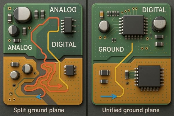
Are you debating between using one large ground plane or splitting it into analog and digital sections? Making the wrong choice can force high-frequency power noise directly into your sensitive signal return paths, defeating the purpose of separation.
A single, solid ground plane is generally the best strategy, provided you maintain strict partitioning of component placement. Placing all digital components and routing in one area and all analog in another prevents high-frequency digital return currents from flowing under the analog section and corrupting analog signals.
The Case for a Unified and Partitioned Ground Plane
The idea behind splitting a ground plane is to isolate the noisy digital ground from the quiet analog ground. However, this is a dangerous practice that often creates more problems than it solves. If any signal trace has to cross the split, its return current is forced to make a huge detour, creating a massive loop inductance. This loop acts as a slot antenna, radiating EMI and making the signal highly susceptible to noise.
The superior approach is to use a unified ground plane and enforce disciplined layout partitioning. Think of your ground plane as a country and the return currents as traffic. You don't want heavy truck traffic (digital currents) driving through a quiet residential neighborhood (analog section). By placing all your digital components in one "city" and all your analog components in another, their respective return currents will naturally stay underneath their signal traces and remain within their own regions. This ensures the digital noise is contained within the digital area.
| Grounding Strategy | Pros | Cons | Best For |
|---|---|---|---|
| Single Ground Plane | Provides a continuous, low-impedance return path. Simple to implement. | Requires strict component partitioning to be effective. | Most mixed-signal designs, including high-speed. |
| Split Ground Plane | Can offer high isolation if implemented perfectly. | High risk of creating large return loops (slot antennas). Difficult to route across the split. | Specialized cases, like high-voltage isolation, and only with extreme care. |
| Star Grounding | Connects all grounds at one single point. | Becomes very difficult to manage in complex PCBs; long traces create inductance. | Low-frequency analog circuits; rarely practical for modern digital systems. |
Are you seeing noise coupling between your power supply and high-speed data lines? The problem likely lies in how their return currents share the same ground plane. They don't flow in the same way, and managing this is critical.
To manage shared return paths, you must design for the "path of least impedance," not just least resistance. Provide a direct, low-inductance return path for high-frequency currents directly under their signal traces, while ensuring the high-power DC or low-frequency return path doesn't disrupt this.
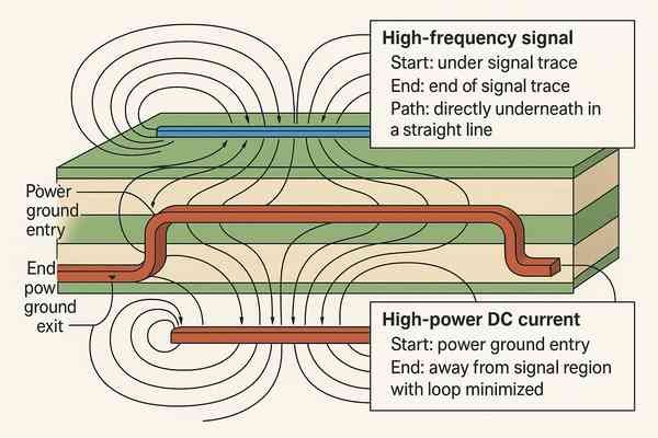
Controlling DC Power Drops and High-Frequency Noise
On a shared ground plane, a DC current and a high-frequency current behave differently. The problem arises when a large DC current creates a voltage drop across the plane. Let's say a 10A current (\(I\)) flows through a path with just 2 \(\text{m}\Omega\) of resistance (\(R\)). That's a 20mV voltage drop (\(V = I \times R\)). If a sensitive analog signal is referenced to this same ground plane, that 20mV of "ground bounce3" is directly added to the signal as noise. This was a key insight I learned while working on large-scale systems at Honeywell; the trace resistance is low, but the return path voltage drop is the real killer.
| Current Type | Primary Concern | Path Taken | Management Strategy |
|---|---|---|---|
| DC / Low-Frequency | Voltage Drop (\(V=I \times R\)) | Path of least resistance (straightest line). | Use wide, heavy copper. Position high-current sources and loads to avoid sensitive areas. |
| High-Frequency AC | Inductance & EMI | Path of least impedance (smallest loop area, under the trace). | Provide a continuous, adjacent reference plane. Use decoupling capacitors4. |
By understanding these different behaviors, you can use component placement and layout partitioning to ensure the paths, while on the same plane, do not interfere with one another.
How Can Guard Traces Effectively Shield Signals on a Heavy Copper PCB?
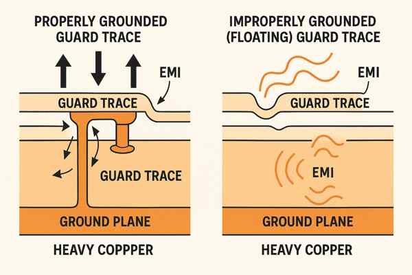
Are you trying to use guard traces to shield sensitive signals but not seeing the expected results? A guard trace that isn't implemented correctly is just another antenna on your board, potentially making noise problems worse.
To be effective, a guard trace must be run parallel to the signal trace and have a solid connection to the signal's reference ground plane with vias stitched along its length. A floating or improperly grounded guard trace is worse than no guard trace at all.
Implementing Guard Traces That Actually Work
A guard trace is intended to intercept electromagnetic fields from an aggressor trace before they can couple to a victim trace. For this to work, the guard trace must provide a lower-impedance path to ground than the victim trace.
| Practice | Principle | Guideline |
|---|---|---|
| Grounding | Provide a low-impedance path for noise. | Connect the guard trace to the signal's reference ground (e.g., Analog Ground). |
| Stitching Vias | Prevent the guard trace from acting as an antenna. | Place grounding vias along the trace, spaced no more than \(\frac{\lambda}{20}\) apart. |
| Trace Spacing | Balance shielding with layout density. | Use the 3W rule: center-to-center spacing is 3x the trace width. |
| Use Case | Know when it is appropriate. | Most effective for low-to-mid frequency analog signals. May negatively impact high-speed digital signals due to added capacitance. |
A properly implemented guard trace, tied to the correct ground with a "picket fence" of vias, creates a coaxial-like shield, protecting the signal from external noise.
What Is the Effect on Signal Integrity When Crossing a Gap in a Power Plane?
Are you routing a signal trace across a split in a ground or power plane? This is one of the most common and critical mistakes in PCB layout, creating a disaster for signal integrity and EMI.
When a signal trace crosses a gap in its reference plane (whether power or ground), the return current path is broken. The current must find a long, circuitous route back to its source, creating a large loop. This dramatically increases inductance, causes a severe impedance discontinuity, and turns your signal trace into an efficient antenna.
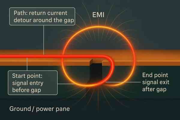
Why Crossing a Plane Gap Creates an EMI Disaster
A high-frequency signal and its return current are a tightly coupled pair. When you route that trace over a split, the return current is forced to detour around the gap. For a 50 \(\Omega\) trace, this discontinuity can make the impedance spike to 150 \(\Omega\) or more, causing massive signal reflections. This creates a host of problems and is a common reason for failing FCC or CE emissions testing. My team once spent a week hunting down an EMI failure that was ultimately traced to a single clock line crossing a 1mm gap between ground planes.
| Solution | How It Works | Best For |
|---|---|---|
| Re-route the trace | The ideal solution. Avoids the problem entirely. | Always the first choice. Never cross a gap if you can avoid it. |
| Stitching Capacitor | Provides a high-frequency "bridge" for the return current across the gap. | When crossing is unavoidable between two different ground planes (e.g., AGND to DGND). |
| Copper Bridge | Creates a single, narrow physical connection point between two planes. | When multiple signals must cross at the same location. Route all traces over this bridge. |
What Via Design Practices Prevent EMI When Signals Pass Through Power Planes?
Are your signals getting noisy after transitioning between layers? Vias are necessary, but if designed poorly, they can act as a point of entry for noise, especially when passing through a high-current power plane.
To prevent EMI, every signal via must have an adjacent "return via" connecting the reference ground planes on the starting and ending layers. This provides a short, continuous path for the return current to follow the signal, minimizing the loop area and preventing noise coupling.
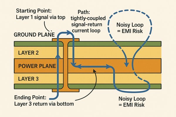
Designing Vias for a Continuous Return Path
When a signal travels down a via, its return current also needs to change layers. Without a dedicated path, the return current will find the nearest available via, creating a large, noise-radiating loop. When passing through a noisy power plane, this makes the signal highly susceptible to picking up that power noise. During a complex photonic computing chip project, we solved a critical signal integrity issue by strategically adding return vias next to every single high-speed signal transition, drastically reducing crosstalk5 and ensuring an on-time release.
| Practice | Principle | Implementation Guideline |
|---|---|---|
| Place Return Vias | Provide a continuous path for the return current. | Place a ground via as close as physically possible to every high-speed signal via (\(<50\) mils). |
| Control Anti-Pads | Prevent capacitive coupling and impedance mismatch. | Ensure adequate clearance around the via in planes. For a 50\(\Omega\) via, anti-pad diameter might be 20-30 mils larger than the via pad. |
| Minimize Stubs | Avoid resonant reflections at high frequencies. | For signals \(>5\) Gbps, use back-drilling to remove the unused portion of the via barrel. |
| Use Via Arrays | Reduce inductance and thermal resistance for power. | For high-current connections, use multiple vias instead of one large one. |
What are the Trade-offs Between Minimizing Voltage Drop and Radiated EMI?
Are you struggling to balance the need for wide traces to handle high currents with the need for tight layouts to control noise? This is a fundamental trade-off in power delivery design.
Wider traces reduce resistance and thus minimize voltage drop (\(V = I \times R\)), which is crucial for power integrity. However, if the return path is not routed closely parallel to the power trace, a wider trace can increase the overall current loop area, which in turn increases radiated EMI.
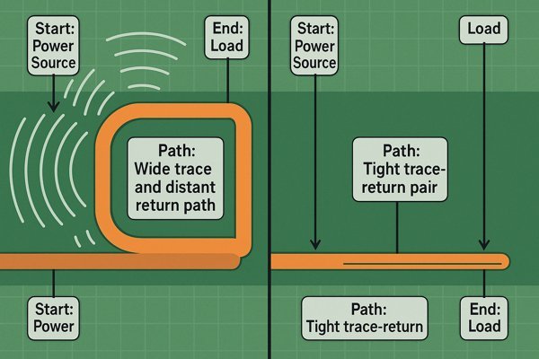
Balancing Low Resistance with Low Radiation
This trade-off forces engineers to think in terms of both DC and AC performance. The solution is to get the benefits of both by minimizing the loop area. You can use a wide, heavy copper trace to minimize voltage drop, but you must ensure its return path is equally wide and runs directly underneath it on an adjacent layer. This creates a low-resistance path while simultaneously creating a very small, low-inductance current loop, effectively containing the magnetic field between the conductors.
| Design Goal | Physical Implementation | Positive Effect | Potential Negative Effect |
|---|---|---|---|
| Minimize Voltage Drop | Use wide, thick copper traces. | Lower \(I \times R\) drop, less heat dissipation (\(P = I^{2}R\)). | Can increase loop area if return path is not controlled. |
| Minimize Radiated EMI | Minimize the area of the current loop. | Less noise radiation, better EMC performance. | Requires careful routing and an adjacent return path. |
Which Filtering Components Best Mitigate Noise on Heavy Copper Boards?
Have you placed decoupling capacitors on your board but still see significant noise on your power rails? With the high currents and fast switching of heavy copper designs, a more robust filtering strategy is often required.
The best approach is a multi-stage filter using a combination of bulk capacitors, a distributed network of ceramic decoupling capacitors, and ferrite beads. This combination effectively creates a low-impedance power distribution network (PDN) across a wide frequency spectrum.
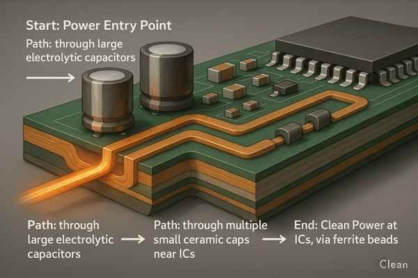
A Three-Stage Filtering Strategy for Clean Power
No single component can solve all noise problems. A strategic combination is needed to create a low-impedance path to ground for noise at all frequencies of concern.
| Component Type | Typical Values | Primary Function | Placement |
|---|---|---|---|
| Bulk Capacitor | 10 \(\mu\text{F}\) – 100 \(\mu\text{F}\) (Tantalum/Electrolytic) | Local energy reservoir; filters low-frequency ripple. | At the point where power enters the board or a specific section. |
| Ceramic Decoupling Network | 0.01 \(\mu\text{F}\), 0.1 \(\mu\text{F}\), 1 \(\mu\text{F}\) | Supplies high-frequency transient currents; broad frequency coverage. | As close as possible to every IC power pin. |
| Ferrite Bead | Varies (e.g., 120 \(\Omega\) @ 100 MHz) | Resistor at high frequencies; dissipates noise energy. | In series with the power trace, before the decoupling capacitors. |
Crucially, you must check the ferrite's datasheet for its impedance curve under DC bias. A bead rated for 3A might lose 90% of its filtering impedance with 1.5A flowing through it. A common rule from Analog Devices is to operate a ferrite bead at only about 20% of its rated DC current to maintain its effectiveness.
Conclusion
High currents on heavy copper boards introduce noise through both magnetic coupling and, more importantly, return path voltage fluctuations. Successfully managing this requires a holistic approach: meticulous partitioning, intelligent layer stack-ups, disciplined grounding, and strategic filtering to ensure power and signals coexist reliably.
-
Understanding the role of dielectric constant is crucial for optimizing PCB designs and ensuring signal integrity. ↩
-
Learn about IPC-2221 guidelines to ensure your PCB design meets industry standards and achieves optimal performance. ↩
-
Understanding ground bounce is crucial for designing circuits that minimize noise and improve performance. Explore this link to learn more. ↩
-
Decoupling capacitors are essential for stabilizing power supply in circuits. Learn how they can enhance your designs. ↩
-
Crosstalk can severely impact signal quality. Discover effective strategies to minimize it and improve your designs. ↩


