 Skip to content
Struggling with messy, damaged board edges after separation? This common manufacturing headache can derail your project. You need a reliable way to depanelize boards without causing stress or defects.
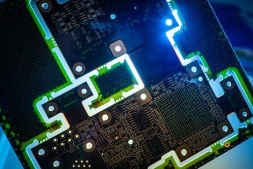
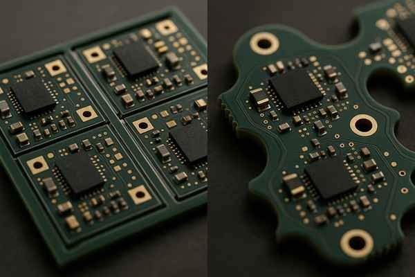
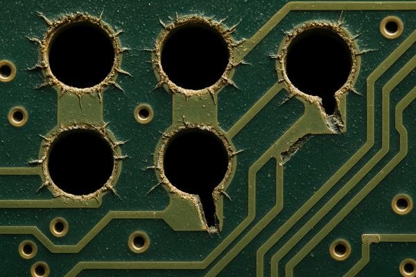
Stamp holes, also known as mouse bites, are a series of small, perforated holes used in PCB manufacturing to connect individual boards within a larger panel. These perforations create a weak point, allowing for easy, clean separation (depanelization) after assembly with minimal stress to the board.
As a hardware engineer for nearly two decades, I've seen countless projects succeed or fail based on manufacturing details. One of the most overlooked yet critical aspects is how we separate individual circuit boards from the main panel. A poor choice here can lead to component damage, high scrap rates, and frustrating delays. Getting the panelization and depaneling strategy right from the start is a simple step that saves immense trouble down the line. Let's dive into how to do that effectively.
What Is PCB Panelization?
Ever wonder how small circuit boards are handled efficiently in mass production? Trying to assemble them one by one would be a nightmare of handling costs and wasted time.
PCB panelization is the manufacturing technique of fabricating multiple smaller, identical, or different PCBs on a single, larger board called a panel or array. This simplifies handling, streamlines the automated assembly process, and significantly reduces production costs and time by processing many boards at once.
Deconstructing the Panelization Strategy
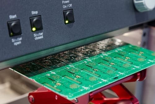
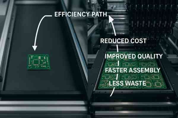
Panelization is a core strategy for efficient electronics manufacturing. Instead of running tiny, individual boards through a pick-and-place machine, we group them. This allows automated equipment to process a large number of boards in a single pass. A standard manufacturing panel is often sized at 18 x 24 inches, and the goal is to maximize its use.
Key Objectives of Panelization
The primary goals are simple but critical. First, maximize material usage. By carefully arranging boards, we minimize the amount of wasted FR-4 laminate, which can reduce material costs by over 20%. Second, optimize assembly throughput. Processing a single panel with 25 boards is vastly faster than handling 25 individual boards. This directly lowers the cost of labor and machine time for stencil printing, SMT placement, reflow soldering, and automated optical inspection (AOI).
Types of Panel Arrays
There isn't a one-size-fits-all approach. The panel layout depends on the project.
| Panel Array Type | Description | Best For |
|---|---|---|
| Homogeneous | The panel contains multiple copies of a single, identical PCB design. | High-volume production of one specific product. |
| Heterogeneous | The panel contains a set of different PCBs that belong to the same overall product (e.g., a main board and a separate display board). | Multi-board products, ensuring all parts are produced in the same batch for consistency. |
This "step-and-repeat" process also ensures consistency, as all boards on a panel experience the same process conditions, improving quality control and overall yield.
Why Are PCBs Manufactured in Panels?
Is it really worth the effort to design a panel? You might think fabricating individual boards is more straightforward, but this approach quickly becomes a bottleneck, driving up costs and slowing down your timeline.
PCBs are made in panels primarily for economic and logistical efficiency. Panelization drastically speeds up automated assembly, reduces material waste, improves handling stability for smaller boards, and ensures higher, more consistent quality control across a production run, ultimately lowering the cost per board.
The Three Pillars of Panelization Benefits
The "why" behind panelization comes down to the realities of Surface Mount Technology (SMT) assembly lines. These expensive machines are optimized for standard board sizes to move them along conveyor belts. A tiny, 30mm x 30mm board simply cannot be handled by the machinery's clamping and transport systems. Panelization solves this fundamental logistical problem. I break down the advantages into three key pillars.
| Benefit Pillar | Description | Practical Impact |
|---|---|---|
| Throughput & Speed | Processing a full panel in one cycle is much faster than handling individual boards. | Cuts assembly time by 50-75%; reduces labor and machine costs. |
| Cost Reduction | Maximizes the usable area from a bulk laminate sheet, minimizing material scrap. | Lowers per-board cost by 15% or more, as setup fees are amortized over more units. |
| Process Consistency | All boards on a panel experience identical thermal profiles and process parameters. | Improves solder joint quality and reduces batch-to-batch variations, increasing overall yield. |
What Are the Different Methods for Depanelizing PCBs?
You've successfully assembled your panel, but how do you break the boards apart without damaging them? The wrong method can introduce stress, crack components, or leave ugly, rough edges that interfere with enclosures.
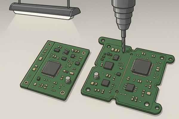
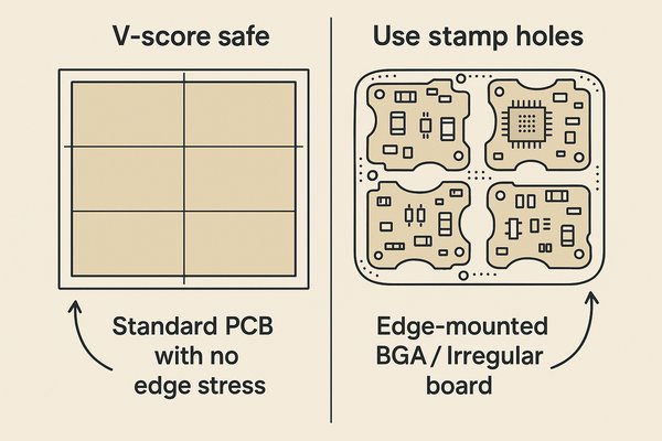
The primary methods for depaneling PCBs are V-scoring (or V-cut), which creates a straight, weakened line for snapping, and tab-routing (using stamp holes or solid tabs), which uses a milling tool to cut the board profile, leaving small tabs to hold it in place.
A Breakdown of Depaneling Techniques
Choosing a depaneling method is a critical design decision. I once saw a project fail pilot production due to micro-cracks in capacitors near a V-score line; a simple switch to tab-routing solved it, but not before causing delays. Understanding the options prevents these costly mistakes.
| Method | Process Description | Stress Level | Best For | Key Limitation |
|---|---|---|---|---|
| V-Scoring | A V-shaped groove is cut ~1/3 deep on the top and bottom of the board. | High | High-volume, rectangular boards. | Only for straight lines; can damage nearby components. |
| Tab-Routing | A router mills the board outline, leaving perforated tabs. | Low | Irregularly shaped boards or designs with sensitive components. | Slower process, higher cost, leaves "mouse bites". |
| Laser Cutting | A high-power laser ablates the PCB material to cut the outline. | Very Low | Ultra-sensitive, flexible, or miniaturized circuits. | Very high cost and slow processing speed. |
| Punching | A custom die set punches the board out of the panel in a single press. | Moderate | Extremely high-volume production. | Requires expensive, non-reusable custom tooling. |
What is the Difference Between Stamp Holes and V-Scoring?
Confused about when to use stamp holes versus a V-cut? Choosing incorrectly can lead to manufacturing failures, especially if your board has a complex shape or sensitive components near the edge.
The key difference lies in flexibility and stress. V-scoring is for straight-line separation of rectangular boards, while stamp holes (tab-routing) support any board shape and put less mechanical stress on the PCB during separation, protecting sensitive components near the edge.
A Head-to-Head Comparison
I've used both extensively, and the decision always comes down to the design's specific needs. At Honeywell, we used V-scoring for high-volume rectangular keypads to keep costs down. At Smiths Medical, for a complex medical pump with edge connectors, tab-routing with stamp holes was non-negotiable to prevent field failures.
| Feature | Stamp Holes (Tab Routing) | V-Scoring (V-Cut) |
|---|---|---|
| Board Shape | Supports any shape (round, L-shape, complex contours). | Only supports straight lines, edge-to-edge. Best for rectangular boards. |
| Component Keep-out | Minimal. Can place components close to the edge, but need to avoid tabs. | Significant. A keep-out of at least 3.81 mm (0.15") from the board centerline is recommended. |
| Mechanical Stress | Low. The breaking force is localized to the small tabs. | High. The snapping action flexes the entire board, risking damage to BGAs or ceramic capacitors. |
| Edge Finish | Leaves small rough patches ("mouse bites") that may require sanding. | Leaves a relatively clean but potentially sharp edge along the entire break line. |
| Panel Space Usage | Less efficient. Requires a router channel, typically 1.6 mm to 2.4 mm, between boards. | More efficient. Boards can be placed directly adjacent (zero-gap), maximizing panel density. |
When Should I Use Stamp Holes Instead of V-Scoring?
Unsure if the benefits of stamp holes justify the extra cost for your project? Making the wrong call could lead to damaged boards or an inefficient panel layout, wasting time and money.
Use stamp holes when your PCB is not rectangular, has components close to the edge (less than 3mm), or features sensitive components like BGAs or large ceramic capacitors that could be damaged by the mechanical stress of V-score breaking.
A Critical Design Checklist
The decision to use stamp holes is a risk-management choice. While it adds cost, it buys you insurance against mechanical damage. I use this decision matrix to make the call.
| Design Consideration | Question to Ask | Recommendation if "Yes" | Rationale |
|---|---|---|---|
| Board Shape | Is the board outline non-rectangular? | Use Stamp Holes | V-Scoring only works on straight lines. |
| Component Proximity | Are there sensitive components (capacitors, BGAs) within 3mm of the edge? | Use Stamp Holes | Isolates components from the high stress of V-score snapping. |
| Edge Features | Does the board have castellated holes or edge connectors? | Use Stamp Holes | V-Scoring would destroy these features. |
| Board Thickness | Is the PCB very thin (< 0.8mm) or flexible? | Use Stamp Holes | Provides better structural support and a more controlled break. |
What Are the Design Guidelines for Stamp Holes on a PCB?
Poorly designed stamp holes can make boards hard to separate or too fragile to survive assembly. You need specific, proven guidelines to ensure they work perfectly every time.
For reliable stamp holes, use 5 non-plated-through (NPTH) holes per tab, each with a diameter of 0.5mm to 0.8mm. Space the holes about 1.0mm to 1.5mm apart (center-to-center). Place tabs roughly every 50mm to 75mm along the board edge for stability.
Engineering a Perfect Break: Key Parameters
Getting stamp hole design right is a balancing act between panel strength and ease of separation. Adhering to industry standards is key. Here are the specific parameters I follow, which align with IPC-2222 guidelines1. It is also critical to avoid placing tabs directly in sharp corners; instead, place them on the straight sections leading into and out of the corner.
| Parameter | Recommended Value | Rationale |
|---|---|---|
| Hole Type | Non-Plated Through-Hole (NPTH)2 | Plated holes add significant strength and are difficult to break, defeating the purpose. |
| Hole Diameter | 0.5mm - 0.8mm (0.020" - 0.031") | 0.6mm (0.024") is a good starting point. Smaller holes break cleaner but make the panel weaker. |
| Hole Spacing | 1.0mm - 1.5mm (center-to-center) | This spacing ensures the perforations are close enough to create a clean break line. |
| Hole Count per Tab | 3 to 5 holes | Provides a good balance of strength for handling and weakness for breaking. |
| Tab Placement | Every 50mm - 75mm | Distributes support evenly. For heavier boards, place them closer together. |
| Tab Clearance | >1.0mm from copper traces | Prevents accidental damage to circuitry during routing or breaking. |
| Router Channel | 1.6mm (0.063") or 2.4mm (0.094") | This space is required for the router bit. Always confirm with your specific fabricator. |
How Do Stamp Holes Affect the Cost of PCB Manufacturing?
Worried that using stamp holes will blow your budget? While they add cost, understanding where that cost comes from helps you decide if the expense is justified for your design's reliability.
Stamp holes increase PCB manufacturing costs because they require an additional CNC routing step to cut the board profile, which takes more machine time than V-scoring. They also slightly reduce panel space efficiency, meaning fewer boards per panel, which increases the per-board cost.
A Cost Driver Analysis
The cost increase from using stamp holes is not arbitrary; it's directly tied to specific manufacturing resources. The combined impact is typically a 15% to 30% higher fabrication cost compared to a V-scored equivalent.
| Cost Driver | V-Scoring | Tab-Routing with Stamp Holes | Financial Impact |
|---|---|---|---|
| Machine Time | Very fast (10-20 sec/panel). | Slow (2-5 min/panel). | Major. More machine time directly increases cost. |
| Material Yield | Very high (zero-gap between boards). | Lower (requires 1.6-2.4mm channel). | Moderate. Fewer boards per panel increases the per-unit material cost. |
| Tooling/Setup | Minimal setup. | Requires CNC programming for the router path. | Minor. |
| Consumables | Minimal blade wear. | Router bits are consumables and require replacement. | Minor. |
What Are the Potential Defects Associated with Stamp Holes?
Even with a good design, things can go wrong. If you don't know what to look for, you might end up with boards that have rough edges, stress fractures, or are difficult to separate, causing production headaches.
The main defects from stamp holes are rough, jagged edges (burrs or "mouse bites") after separation that may require manual sanding, and potential stress on the board if tabs are too strong or broken improperly, which can damage nearby traces or laminate.
Common Failure Modes and Their Causes
Knowing the potential failure modes is key to preventing them. When I review a new design that uses stamp holes, I'm specifically looking for risks in three areas.
| Defect Category | Description | Common Causes | Consequence |
|---|---|---|---|
| Edge Finish Defects | Rough, jagged "mouse bites" where tabs were broken. | Tabs too thick; holes too large; improper twisting motion during separation. | Requires costly manual sanding; can interfere with mechanical assembly. |
| Laminate/Component Stress | Micro-fractures in the PCB substrate or solder joints. | Tabs are too strong (e.g., plated holes); aggressive breaking without support. | High Risk. Can cause latent, hard-to-diagnose field failures. |
| Panel Integrity Issues | The entire panel is too flimsy and sags or vibrates during assembly. | Tabs are too weak (too far apart or too perforated). | Inconsistent solder paste application and component placement errors. |
How Are PCBs with Stamp Holes Separated?
You have your assembled panel, but what's the right way to break it apart? Just snapping it over the edge of a desk is asking for trouble and can lead to broken components or boards.
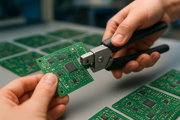
PCBs with stamp holes are separated using manual or automated methods. Manually, a technician can use their hands with a fixture for support or a specialized hand-held "nibbler" tool. For higher volumes, automated depaneling routers or punching systems are used for consistency.
Comparing Separation Techniques
The separation method must match the production scale and the sensitivity of the design. Choosing the wrong one can undo all the benefits of using stamp holes in the first place. For any production units, I strongly advise against breaking by hand. For low volumes, a manual nibbler ($100-$300) is a great investment. For mass production, automation is the only way to ensure consistency.
| Method | Volume | Speed | Edge Quality | Stress Level | Relative Cost |
|---|---|---|---|---|---|
| By Hand | Prototype Only | Fast | Poor | Very High | Free |
| Manual Nibbler | Low | Moderate | Good | Low | Low |
| Auto. Router | Medium-High | Slow | Excellent | Very Low | High |
| Auto. Punch | Very High | Very Fast | Very Good | Moderate | Very High |
Are There Automated Tools for Depaneling Boards with Stamp Holes?
Is manual depaneling slowing down your production line? As volume scales up, you need a faster, more reliable solution that eliminates human error and ensures consistent quality for every board.
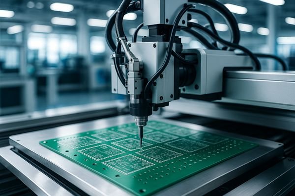
Yes, several automated tools exist for depaneling tab-routed PCBs. These include CNC depaneling routers that mill away the tabs for a smooth finish, and automated punching systems that use a custom die to separate boards quickly, ideal for high-volume manufacturing.
A Look at High-Volume Depaneling Systems
Automated depaneling is essential for scaling production. The two primary types of automated tools—routers and punching systems—serve very different needs in the manufacturing world.
| Feature | Automated Depaneling Router | Automated Punching System |
|---|---|---|
| Mechanism | A CNC-controlled spindle with a router bit mills away tabs. | A custom die set punches all boards out in a single stroke. |
| Ideal Volume | Medium to High (e.g., 1,000-100,000 units) | Very High (e.g., 100,000+ units) |
| Speed | Slow (2-5 minutes per panel) | Extremely Fast (1-2 seconds per panel) |
| Edge Quality | Excellent, smooth finish. | Very good, but can have slight shock marks. |
| Flexibility | Very High. Reprogram for any board design. | Very Low. Requires a new, expensive die for each design. |
| Tooling Cost | Low (only consumable router bits). | Very High ($5,000 - $20,000+ per die set). |
Conclusion
Choosing the right panelization method, like stamp holes, is a small detail that has a huge impact on manufacturing efficiency, quality, and cost. Get it right, and your project runs smoothly.


