 Skip to content
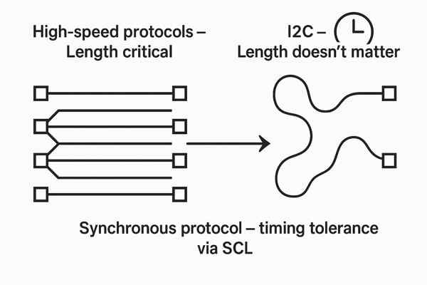
Are you worried about meticulously matching the lengths of your \(SCL\) and \(SDA\) lines? You're not alone. Many engineers spend time on this, but it's often unnecessary and distracts from the real issues that can cripple your I2C bus.
No, I2C does not generally require trace length matching. Because I2C operates at relatively low speeds (typically \(100 \text{ kHz}\) or \(400 \text{ kHz}\)), the signal wavelength is much longer than the trace lengths on a typical PCB. The protocol's timing is tolerant of the small propagation delay differences that result from mismatched lengths.

This might seem counterintuitive, especially if you're used to high-speed interfaces where every millimeter counts. The key is understanding that I2C was designed for simplicity and short-range communication on a single board. Instead of focusing on trace length, your attention should be on the true performance-limiting factor: the total capacitance of the bus. Let's explore why this is the case and how to design a robust I2C interface.
Why Doesn't I2C Require Length Matching?
Struggling to understand why some buses need perfect length matching while I2C doesn't? It can be confusing, but the reason lies in the protocol's fundamental design and timing.
I2C does not require length matching because it is a synchronous protocol where data transitions on the \(SDA\) line are qualified by the level of the \(SCL\) line, not by a precise clock edge. Data is valid for the entire \(SCL\) high period, a very generous window at typical I2C speeds.
To truly grasp this, we need to break down the timing and electrical characteristics of the bus. The protocol's low speed and level-sensitive nature create a forgiving environment where picoseconds of delay mismatch from trace length are irrelevant. In my experience, focusing on length matching here is a classic case of solving the wrong problem. Let's dig into the specifics.
Understanding I2C Timing
The I2C protocol1 defines that data on the \(SDA\) line only changes when the \(SCL\) clock line is low. The data must be held stable for the entire duration that \(SCL\) is high. This creates a very large "data valid" window. Unlike high-speed interfaces that latch data on a specific clock edge (rising or falling), I2C just needs the data to be stable during the \(SCL\) high pulse. For a \(100 \text{ kHz}\) signal, this high period is about \(4 \text{ µs}\). A propagation delay2 difference of a few picoseconds due to mismatched trace length is insignificant within this massive window.
The Role of Signal Speed and Wavelength
At \(100 \text{ kHz}\), the electrical wavelength of the signal is kilometers long. On a PCB that is only a few centimeters in size, the traces are electrically very short. This means the signal appears at all points on the trace almost instantaneously. There's no risk of running into transmission line effects where impedance matching and length tuning become critical. The small propagation delay (typically around \(150 \text{ ps/inch}\) on FR-4) is negligible compared to the protocol's timing requirements.
Comparing Timing Budgets
| Parameter | I2C (\(100 \text{ kHz}\) Standard-mode) | High-Speed Interface (e.g., DDR4) |
|---|---|---|
| Timing Basis | Level-sensitive (\(SCL\) high/low) | Edge-sensitive (Clock edge) |
| Timing Window | \(\approx 4,000,000 \text{ ps}\) (\(4 \text{ µs}\)) | \(< 625 \text{ ps}\) |
| Sensitivity to Skew | Extremely Low | Extremely High |
| Length Matching | Not required | Critical |
What is the Primary Limiting Factor for I2C Performance if Not Trace Length?
If trace length isn't the main concern, what should you be focusing on? Many designs fail not because of length mismatch, but because of a factor that is often overlooked during layout.
The primary limiting factor for I2C performance is the total bus capacitance (\(C_{BUS}\)). This capacitance, formed by PCB traces, component pins, and connectors, directly dictates the maximum speed and reliability of your bus by slowing down the signal's rise time.
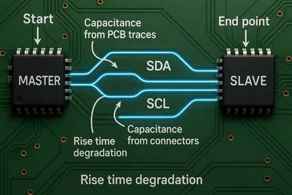
The open-drain nature of I2C is the key to understanding this. Devices can only pull the line low; they can't drive it high. A pull-up resistor does the work of pulling the line high, and it must fight against all the parasitic capacitance on the bus. The more capacitance you have, the slower the signal rises, and the more likely your communication is to fail.
The RC Time Constant in I2C
The pull-up resistor (\(R_{P}\)) and the total bus capacitance (\(C_{BUS}\)) form a simple RC circuit. The signal's rise time is directly governed by the time constant of this circuit, \(\tau = R_{P} \times C_{BUS}\). A larger capacitance or a larger resistance means a longer time constant and a slower rise time. If this rise time exceeds the limits defined in the I2C specification, the bus will fail. This is why the official NXP I2C specification (UM10204) puts a hard limit of \(400 \text{ pF}\) on the bus for Standard and Fast modes.
Sources of Bus Capacitance
Total bus capacitance is the sum of all individual capacitances from every element connected to the line. It's crucial to account for all of them.
| Capacitance Source | Typical Value | Notes |
|---|---|---|
| IC Pin Capacitance | \(3 - 10 \text{ pF}\) per pin | Check the device datasheet. |
| PCB Trace Capacitance | \(0.5 - 1.0 \text{ pF}\) per cm | Depends on trace width and distance to ground plane. |
| Via Capacitance | \(0.5 - 1.0 \text{ pF}\) per via | Minimize vias on I2C lines. |
| Connector/Cable Capacitance | \(40 - 100 \text{ pF}\) per meter | A major contributor for off-board connections. |
Impact on Signal Rise Time
A slow rise time effectively shrinks the valid timing window for the rest of the protocol. It can lead to setup time violations and makes the bus more susceptible to noise, as the signal spends more time transitioning through the undefined voltage region between logic low and logic high.
What Are the Recommended PCB Layout Best Practices for I2C?
Feeling uncertain about how to route your I2C lines for maximum reliability? Following a few key best practices can prevent noise, signal integrity issues, and communication failures down the line.
The best practices for I2C layout are to use strong pull-up resistors, keep traces as short and direct as possible, place pull-ups close to the master device, and use a solid ground plane to control impedance and minimize noise.
I've debugged many I2C issues that came down to poor layout, not a faulty component. A little foresight during the layout phase saves hours of frustration with an oscilloscope later. The goal is simple: minimize capacitance and noise coupling. This is achieved through careful component placement, disciplined trace routing, and proper use of the ground plane.
Strategic Component Placement
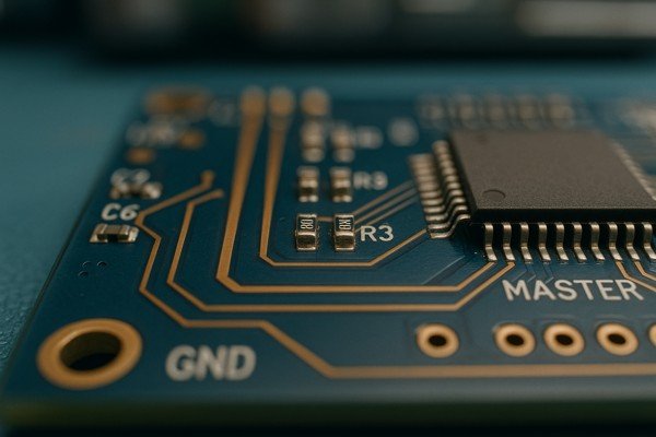
Where you place your components is the first step. Grouping I2C devices minimizes the required trace length, which in turn reduces trace capacitance. The pull-up resistors should be placed near the bus master (usually the microcontroller). This isn't a strict rule, but it provides a good reference point and ensures the pull-ups are centrally located.
Trace Routing and Shielding
Route the \(SDA\) and \(SCL\) lines as a pair, keeping them parallel and close together. This helps ensure they experience similar environments, improving common-mode noise rejection3. Keep them far away from high-frequency or high-current switching signals—a clearance of \(3\times\) the trace width is a good rule of thumb. Avoid vias whenever possible, as each one adds unwanted capacitance.
Key Layout Guidelines
| Guideline | Do | Don't |
|---|---|---|
| Routing | Keep traces short and direct. Route \(SDA\)/\(SCL\) as a parallel pair. | Use long, meandering traces. Create loops. |
| Grounding | Route over a solid, unbroken ground plane. | Route over splits or voids in the ground plane. |
| Placement | Group I2C devices. Place pull-ups near the master. | Scatter components across the board. |
| Noise | Maintain clearance from noisy signals (clocks, SMPS). | Route I2C lines parallel to high-speed signals. |
| Vias | Minimize or eliminate vias. | Use multiple vias unnecessarily. |
When Should Trace Length and Signal Integrity Become a Concern in an I2C Design?
Are you pushing the limits of your I2C bus? While typically robust, there are specific scenarios where you must pay closer attention to length and signal integrity to avoid problems.
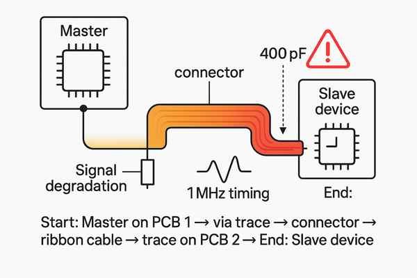
Trace length becomes a concern when the total bus capacitance approaches the \(400 \text{ pF}\) limit, when operating at higher speeds like Fast-mode Plus (\(1 \text{ MHz}\)), or when routing I2C between separate PCBs connected by a cable.
While I've stressed that length matching isn't needed, this doesn't mean length is irrelevant. The absolute length of your traces directly contributes to the total bus capacitance. There are clear red flags in a design that tell me it's time to move from simple best practices to active signal integrity analysis.
Crossing the On-Board Boundary
The moment the I2C bus leaves a single PCB and travels over a cable or connector, you must be concerned. Cables have significantly higher capacitance per unit length than PCB traces. A \(30 \text{ cm}\) ribbon cable can easily add \(20-30 \text{ pF}\) to your bus, which could be a significant portion of your total \(400 \text{ pF}\) budget. In these cases, using an I2C bus buffer or extender IC (like the P82B715) is often the only reliable solution.
Pushing Speed Limits
The timing margins for higher speed modes are much tighter.
| I2C Mode | Max Rise Time | Design Focus |
|---|---|---|
| Standard (\(100 \text{ kHz}\)) | \(1000 \text{ ns}\) | Very forgiving. |
| Fast (\(400 \text{ kHz}\)) | \(300 \text{ ns}\) | Must manage capacitance. |
| Fast-mode+ (\(1 \text{ MHz}\)) | \(120 \text{ ns}\) | Layout and low capacitance are critical. |
| Hs-mode (\(3.4 \text{ MHz}\)) | \(120 \text{ ns}\) | Requires active pull-ups and careful design. |
When you move to Fast-mode Plus or higher, the reduced rise time budget means even small amounts of extra capacitance from longer traces can cause failures.
High-Noise Environments
If your board is operating in an electrically noisy environment (e.g., industrial motor control, automotive), long I2C traces act as effective antennas. They will pick up noise that can corrupt the data on the bus. In these situations, keeping traces as short as physically possible is your best defense. Shielding the traces with ground planes and considering the use of ferrite beads for filtering also becomes important.
How Are the Correct Pull-Up Resistor Values for an I2C Bus Calculated?
Choosing the wrong pull-up resistors is a common source of I2C failures. It can lead to slow signals that don't work or signals that can't be pulled low, causing the bus to fail.
The correct pull-up resistor value is a trade-off. It must be low enough to provide a fast signal rise time but high enough to not exceed the sink current capability of the I2C devices when pulling the line low.
I've seen designs fail for something as simple as using a \(10 \text{ k}\Omega\) resistor when a \(2.2 \text{ k}\Omega\) was needed. Calculating the valid range is straightforward and should be a mandatory step for any I2C design. The calculations for the minimum and maximum resistance values are derived directly from the official NXP I2C specification.
Calculating the Minimum Resistance (\(R_{P(min)}\))
The minimum resistance is set by the maximum current the I2C device drivers can sink (\(I_{OL}\)) while maintaining a valid low voltage level (\(V_{OL(max)}\)). Choosing a resistor value below this minimum will prevent the devices from pulling the line all the way down to a logic '0'.
\(R_{P(min)} = \frac{V_{DD} - V_{OL(max)}}{I_{OL}}\)Calculating the Maximum Resistance (\(R_{P(max)}\))
The maximum resistance is determined by the need to charge the bus capacitance (\(C_{BUS}\)) fast enough to meet the protocol's rise time requirement (\(t_{r}\)). Choosing a resistor value above this maximum will cause the signal rise time to be too slow, leading to communication errors.
\(R_{P(max)} = \frac{t_{r}}{0.8473 \times C_{BUS}}\)A Practical Calculation Example
Let's calculate the range for a common scenario: a \(3.3\text{ V}\) system running in Fast-mode (\(400 \text{ kHz}\)) with an estimated bus capacitance of \(100 \text{ pF}\).
| Parameter | Symbol | Value | Source |
|---|---|---|---|
| Supply Voltage | \(V_{DD}\) | \(3.3 \text{ V}\) | System Requirement |
| Max Low Voltage | \(V_{OL(max)}\) | \(0.4 \text{ V}\) | I2C Specification |
| Max Sink Current | \(I_{OL}\) | \(3 \text{ mA}\) | I2C Specification (Standard) |
| Max Rise Time | \(t_{r}\) | \(300 \text{ ns}\) | I2C Spec (Fast-mode) |
| Bus Capacitance | \(C_{BUS}\) | \(100 \text{ pF}\) | Estimation |
| Calculation | |||
| Min Resistance | \(R_{P(min)}\) | \(\frac{3.3\text{V} - 0.4\text{V}}{0.003\text{A}} = 967 \Omega\) | Formula |
| Max Resistance | \(R_{P(max)}\) | \(\frac{300 \times 10^{-9}\text{s}}{0.8473 \times 100 \times 10^{-12}\text{F}} \approx 3540 \Omega\) | Formula |
Conclusion: A standard value between \(967 \Omega\) and \(3.54 \text{ k}\Omega\) is acceptable. A \(2.2 \text{ k}\Omega\) or \(3.3 \text{ k}\Omega\) resistor would be a safe and common choice.
What Are the Consequences if I2C Traces Are Too Long?
Ignoring trace length limits can seem harmless on the schematic, but it leads to real-world hardware failures that are frustrating to debug. These issues all stem from one root cause: excessive bus capacitance.
If I2C traces are too long, the increased bus capacitance will cause slow signal rise times. This leads to violations of protocol timing, data corruption, and ultimately, complete communication failure between the master and slave devices.
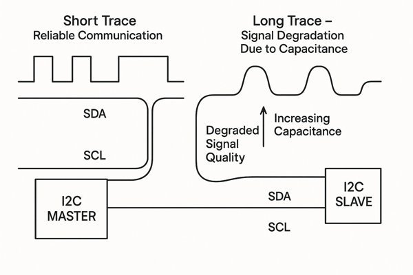
When an I2C bus fails, the symptoms can be confusing. The master might not get an acknowledgment (\(ACK\)), data might be read incorrectly, or the bus might get stuck in a busy state. I've found that tracing these protocol-level problems back to their physical root cause is key. Long traces directly cause waveform degradation, which in turn causes the protocol to fail.
Waveform Degradation
The most direct consequence is a "rounded" or slow rising edge on your \(SCL\) and \(SDA\) signals. Instead of a crisp, sharp transition from low to high, the voltage slowly ramps up. You can see this clearly on an oscilloscope. This slow edge spends more time in the indeterminate logic region, making it vulnerable to noise.
Protocol Timing Violations
The I2C specification4 has strict timing requirements. A slow rise time can directly cause these to be violated.
| Physical Cause | Electrical Effect | Protocol-Level Consequence |
|---|---|---|
| Long Trace \(\rightarrow\) High \(C_{BUS}\) | Slow Rise Time (\(t_{r}\)) | Exceeds max \(t_{r}\) specified (e.g., \(> 300\text{ns}\) for Fast-mode). |
| Slow Rise Time (\(t_{r}\)) | Signal not reaching \(V_{IH}\) in time | Setup time (\(t_{SU;DAT}\)) violation. Master reads incorrect data. |
| Slow Rise Time (\(t_{r}\)) | Bus fails to rise before timeout | Master does not detect slave's \(ACK\) bit, leading to communication abort. |
Increased Noise Susceptibility
Long traces are not just capacitors; they are also antennas. They are more effective at picking up noise from adjacent signals (crosstalk) and external sources (EMI). When this noise is coupled onto a signal that has a slow rise time, it can easily cause false transitions, corrupting the data being transmitted. A short, clean trace with a fast rise time is far more robust.
How Does I2C's Tolerance to Length Mismatch Compare to Other Protocols Like SPI?
Wondering why your SPI layout requires more care than your I2C layout? The difference in tolerance comes down to the fundamental electrical and protocol-level design choices of each interface.
I2C is significantly more tolerant of length mismatch than SPI. I2C's open-drain topology and level-based timing are forgiving, whereas SPI's push-pull drivers and edge-triggered timing make it more sensitive to propagation delays and signal integrity at higher speeds.
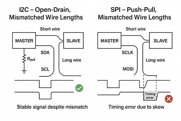
Having designed with both protocols extensively, I can tell you that the design constraints are completely different. For I2C, my primary thought is "capacitance." For high-speed SPI, my thoughts turn to "timing, skew, and impedance." This difference stems from their core architecture.
Driver Topology: Open-Drain5 vs. Push-Pull6
I2C uses an open-drain driver. Devices can only actively pull the line low. A passive resistor pulls it high. This is slow but allows multiple devices to share the line easily. SPI uses push-pull drivers. The master and slave actively drive the line both high and low. This is much faster and provides a cleaner signal, but it means you can't have multiple masters driving the same line without a more complex configuration.
Timing Model: Level vs. Edge Triggered
This is the most critical difference. I2C timing is based on the level of the clock signal. As long as data is stable when \(SCL\) is high, it's valid. SPI timing is based on the edge of the clock signal. Data is latched precisely on the rising or falling edge of \(SCK\). This makes SPI far more sensitive to skew—the difference in arrival time between the clock and data signals. If the data arrives too late and misses the clock edge, the communication fails. This is why at high SPI speeds (\(>20 \text{ MHz}\)), length matching the lines becomes important.
| Feature | I2C (Inter-Integrated Circuit) | SPI (Serial Peripheral Interface) |
|---|---|---|
| Driver Type | Open-Drain: Slow, shared bus friendly. | Push-Pull: Fast, better signal integrity. |
| Timing | Level-sensitive: Data valid when \(SCL\) is high. | Edge-sensitive: Data sampled on a specific \(SCK\) edge. |
| Speed | Typically \(< 1 \text{ MHz}\) | Can exceed \(50-100 \text{ MHz}\) |
| Sensitivity to Skew | Low: Insensitive to minor propagation delay differences. | High: Becomes critical at high clock speeds. |
Are There Special Considerations for High-Speed I2C Modes?
Planning to use I2C at \(1 \text{ MHz}\) or faster? While the core principles remain the same, the reduced timing margins for high-speed modes require a more rigorous design approach to ensure reliability.
Yes, high-speed I2C modes require stricter control over bus capacitance and the use of stronger (lower value) pull-up resistors. For High-Speed Mode (\(Hs\)-mode at \(3.4 \text{ MHz}\)), an active pull-up or bus buffer is often necessary to meet the fast rise time requirements.
In my experience, moving from Standard-mode to Fast-mode Plus (\(Fm+\)) or High-speed mode (\(Hs\)-mode) is not a trivial change. You can't just change the clock frequency in software and expect it to work. The physical layer design must be much more robust.
Requirements for Fast-mode Plus (\(1 \text{ MHz}\))
For \(Fm+\), the main change is the dramatically reduced rise time budget. This forces the use of much lower pull-up resistor values, which in turn requires that the I/O pins on your devices have a higher current sink capability (\(20 \text{ mA}\) vs. \(3 \text{ mA}\) for Standard-mode). You must verify that your MCU and all slave devices are \(Fm+\) compatible. Layout becomes more critical, as every picofarad of stray capacitance eats into your shrinking timing budget.
Challenges of High-Speed Mode (\(3.4 \text{ MHz}\))
\(Hs\)-mode is a different beast entirely. It's not possible to meet the rise time requirements at \(3.4 \text{ MHz}\) with standard passive pull-up resistors. The protocol requires that the master device provides an active, high-current pull-up during the rising edge to charge the bus capacitance quickly. This requires a master device specifically designed for \(Hs\)-mode. Communication also starts at a slower speed, and the master sends a special "master code" to enable \(Hs\)-mode on compatible slave devices.
| I2C Mode | Max Rise Time | Max \(C_{BUS}\) | \(I_{OL}\) Required | Key Consideration |
|---|---|---|---|---|
| Standard (\(100\text{kHz}\)) | \(1000 \text{ ns}\) | \(400 \text{ pF}\) | \(3 \text{ mA}\) | Very flexible. |
| Fast (\(400\text{kHz}\)) | \(300 \text{ ns}\) | \(400 \text{ pF}\) | \(3 \text{ mA}\) | Must manage capacitance. |
| Fast-mode+ (\(1\text{MHz}\)) | \(120 \text{ ns}\) | \(550 \text{ pF}\) | \(20 \text{ mA}\) | Requires \(Fm+\) compatible parts and strong pull-ups. |
| \(Hs\)-mode (\(3.4\text{MHz}\)) | \(120 \text{ ns}\) (effective) | \(400 \text{ pF}\) | \(3 \text{ mA}\) | Requires active pull-up from an \(Hs\)-mode master. |
What Tools Are Available to Check for Potential I2C Signal Integrity Issues?
How can you be sure your I2C bus is healthy before you go to production? Relying on guesswork is risky. Fortunately, several tools can help you verify and debug your I2C interface with confidence.
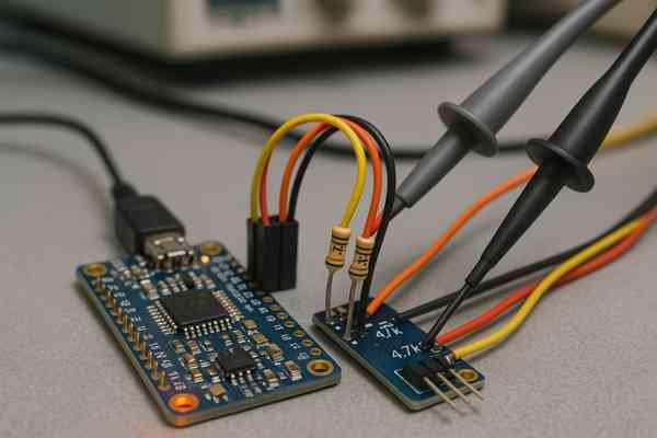
An oscilloscope with serial decoding capability is the most essential tool for checking I2C signal integrity. For more complex issues, a logic analyzer or a dedicated I2C protocol analyzer provides deeper insight into the data communication.
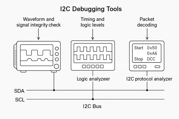
In my lab, I have a suite of tools I rely on. You don't always need the most expensive equipment, but you need the right tool for the job. Trying to debug a timing issue without an oscilloscope is like trying to find a wiring problem in the dark.
The Essential: The Oscilloscope
This is your first and most important tool. It allows you to see the analog reality of the signals on the bus. You can directly measure rise times, check for valid logic levels (\(V_{IL}\), \(V_{IH}\)), and spot problems like noise, ringing, and crosstalk. Modern scopes with I2C protocol decoding (from brands like Keysight, Tektronix, Rohde & Schwarz) are invaluable, as they translate the ones and zeros into human-readable addresses and data right on the screen.
The Detective: The Logic/Protocol Analyzer7
When the problem is more about the conversation than the signal quality, a logic or protocol analyzer is key. These tools capture long sequences of digital data, making it easy to debug complex transactions involving multiple slaves or to find protocol violations that occur intermittently. Tools from Saleae or Total Phase are popular choices here.
The Predictor: Simulation Tools
For high-speed or mission-critical designs, you shouldn't wait for a physical prototype to find problems. Signal integrity simulation tools (like HyperLynx, Cadence Sigrity, or tools within Altium Designer) let you model your PCB layout and predict the I2C bus performance. You can experiment with different trace lengths and pull-up values to optimize the design before manufacturing.
| Tool Type | Best For | What It Tells You |
|---|---|---|
| Oscilloscope | Analog Signal Validation | Rise/Fall Times, Voltage Levels, Noise, Ringing |
| Logic/Protocol Analyzer | Digital Protocol Debugging | Data Content, \(ACK\)/\(NACK\), Start/Stop Conditions, Timing |
| Simulation Software | Pre-Layout Design Verification | Predicted Rise Times, Eye Diagrams, Crosstalk Analysis |
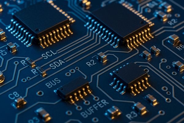
Can an Example of a Good Versus a Bad I2C Layout Be Provided?
Seeing the difference between a good and bad layout can make the best practices much clearer. A bad layout introduces parasitic capacitance and noise paths, while a good layout minimizes them.
A good I2C layout features short, direct traces on a single layer with a solid ground plane underneath and pull-ups near the master. A bad layout uses long, meandering traces, unnecessary vias, and lacks a proper ground reference.
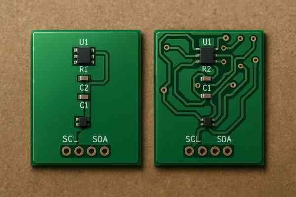
I've seen both extremes in my career. The good designs work reliably across temperature and voltage variations. The bad designs are a constant source of intermittent failures that are a nightmare to track down. The difference is entirely in the physical implementation.
Anatomy of a Good Layout
A good layout is disciplined and prioritizes the integrity of the I2C signals. The designer has clearly thought about minimizing capacitance and providing a clean return path for the signal current. It looks clean and organized because the electrical principles it follows are clean and organized.
Anatomy of a Bad Layout
A bad layout is often the result of treating the I2C lines as unimportant "slow" signals that can be routed last, snaking them around whatever obstacles are in the way. This approach ignores the underlying physics and leads directly to high capacitance, noise pickup, and a bus that is, at best, unreliable.
| Layout Aspect | Good I2C Layout (Robust & Reliable) | Bad I2C Layout (Intermittent & Failing) |
|---|---|---|
| Component Placement | I2C devices grouped closely. Pull-ups near the master. | Devices scattered. Pull-ups placed far from the master. |
| Trace Routing | Short, direct traces. \(SDA\)/\(SCL\) routed as a parallel pair. | Long, meandering traces. \(SDA\)/\(SCL\) take different paths. |
| Ground Plane | Solid, continuous ground plane directly under traces. | Traces routed over splits or voids in the ground plane. |
| Vias | No vias, or a minimal number with grounding vias nearby. | Multiple vias used, increasing parasitic capacitance. |
| Noise Avoidance | Routed away from noisy power supplies or high-speed clocks. | Routed directly over or parallel to noisy signals. |
Conclusion
In short, don't lose sleep over matching the lengths of your I2C traces. Instead, focus your energy on managing the total bus capacitance by keeping traces short and providing properly calculated pull-up resistors.
-
Understanding the I2C protocol is crucial for designing effective communication between devices in embedded systems. ↩
-
Learn about propagation delay to grasp its impact on signal integrity and timing in electronic circuits. ↩
-
Exploring techniques for common-mode noise rejection can lead to more robust and reliable electronic designs. ↩
-
Exploring the I2C specification will provide insights into its timing requirements, ensuring your designs meet necessary standards. ↩
-
Understanding Open-Drain is crucial for grasping how I2C allows multiple devices to share a bus effectively. ↩
-
Exploring Push-Pull drivers will help you understand the advantages of SPI in terms of speed and signal integrity. ↩
-
A Logic/Protocol Analyzer is vital for troubleshooting digital communications. Learn more about its functionalities and advantages here. ↩


