 Skip to content
Struggling with unexpected EMI failures in your designs? Your PCB traces might be radiating noise without you realizing it. Understanding when a simple copper trace turns into an unintentional antenna is key to passing compliance testing and ensuring your product works reliably.
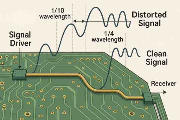
A PCB trace starts to act as an efficient antenna when its length approaches a significant fraction of the signal's wavelength, typically at or above \(1/4\) of the wavelength. For high-frequency signals, which are defined not just by the clock rate but by the signal's rise time, even short traces can become problematic radiators, causing electromagnetic interference (EMI) and failing regulatory tests.

It’s a frustrating experience to have a functionally perfect design fail EMC testing. I’ve been there. You're confident in your circuit, but it radiates too much energy. This is often because we overlook the fact that at high frequencies, every trace is a potential antenna. Let's break down why this happens and how you can prevent it, ensuring your next project gets to market without costly delays and redesigns.
What is the Relationship Between Trace Length and Wavelength?
Having trouble with signal reflections and noise? The physical length of your PCB traces directly relates to the electrical wavelength of the signals they carry. When trace lengths become a large fraction of the signal's wavelength, problems like ringing and EMI are almost guaranteed.
The relationship is critical: if a trace length is a significant portion of the signal's wavelength (e.g., \(1/10\), \(1/4\)), it can act as an antenna and radiate energy. This also leads to transmission line effects, where impedance mismatches cause signal reflections and degrade signal integrity.
Why Wavelength on a PCB Matters
The core issue is that electricity doesn't travel instantaneously. For a 1 GHz signal, the wavelength is much shorter than you might think, especially on a standard PCB material. When the trace length is comparable to this wavelength, different points on the trace have different voltages at the same time, causing the trace to radiate an electromagnetic field.
The Rule of Thumb for Transmission Lines
A common guideline, referenced in industry standards like IPC-22511, states that once a trace length exceeds \(1/20\)th of the signal's wavelength, it must be treated as a transmission line. This is the point where you must consider its potential to radiate and cause signal integrity issues.
Considering Signal Harmonics
A critical mistake is to calculate wavelength based only on a signal's fundamental frequency. A digital square wave is composed of its fundamental frequency plus a series of odd harmonics2 of decreasing amplitude (\(3f, 5f, 7f, \dots\)). According to Fourier analysis, these harmonics can extend to very high frequencies. A 100 MHz clock signal can have significant EMI-causing energy at 500 MHz and 700 MHz. Therefore, you must calculate the wavelength based on the highest frequency harmonic you need to contain.
| Signal | Fundamental Freq. | Key Harmonic Freq. for EMI | Wavelength on FR-4 @ Harmonic | \(1/20\)th Wavelength (Critical Length) |
|---|---|---|---|---|
| Clock | 100 MHz | 500 MHz (5th Harmonic) | ~293 mm | ~14.6 mm |
| USB 2.0 High-Speed | 240 MHz | \(1.2 \text{ GHz}\) (5th Harmonic) | ~122 mm | ~6.1 mm |
| SATA 3.0 | 3 GHz | \(9 \text{ GHz}\) (3rd Harmonic) | ~16 mm | ~0.8 mm |
What is the Quarter-Wavelength Rule for Antennas?
Wondering why a specific trace length is causing so much EMI? It might be resonating like a perfectly tuned antenna. The quarter-wavelength rule is a fundamental principle in antenna theory that explains this phenomenon and is surprisingly relevant to PCB design.
A conductor becomes a very efficient radiator (antenna) when its length is equal to \(1/4\) of the signal's wavelength. At this length, it forms a resonant circuit with its ground plane, maximizing the conversion of electrical energy into electromagnetic radiation, which is great for intentional antennas but disastrous for EMI.
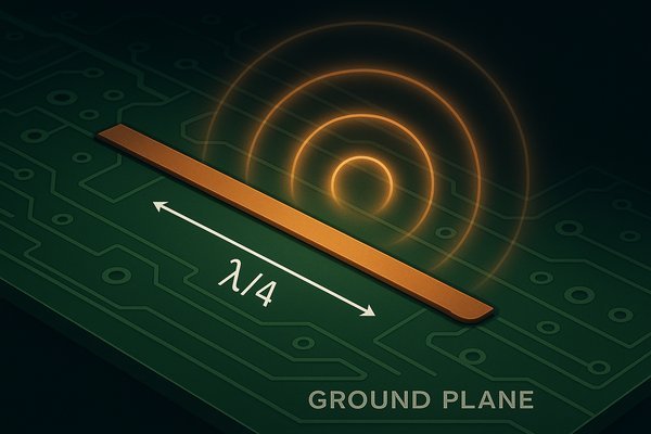
How a Trace Becomes a Resonant Antenna
A quarter-wave monopole antenna3 is a classic example. It uses a ground plane as its reflective surface, effectively creating the other half of a dipole antenna. A PCB trace that happens to be a quarter-wavelength (\(\lambda/4\)) long behaves exactly like this.
The Dangers of Resonance
At its resonant frequency, the trace efficiently converts the signal's energy into electromagnetic waves. This is why clock signals are so problematic; they contain a fundamental frequency and many strong harmonics. If a trace length matches the quarter-wavelength of any of these harmonics, it will broadcast EMI at that frequency.
Beyond Quarter-Wavelength
While the quarter-wave resonance is the most common and efficient for a trace over a ground plane, other lengths are also problematic. A trace that has a poor or distant ground reference can behave more like a half-wave (\(\lambda/2\)) dipole antenna, which resonates strongly when its length is \(\lambda/2\). This is often the case for I/O cables or traces that cross a split in a ground plane. Resonance also occurs at multiples, so a trace can radiate at \(3\lambda/4, \lambda, 5\lambda/4\), etc., though usually with less efficiency than the primary resonance.
How is the Wavelength of a Signal on a PCB Calculated?
Need to know if your trace is electrically long? You can't just use the free-space wavelength. The PCB's material slows the signal down, shortening its wavelength and making even physically short traces electrically significant at lower frequencies than you might expect.
The wavelength (\(\lambda\)) of a signal on a PCB is calculated by dividing the speed of light (\(c\)) by the product of the frequency (\(f\)) and the square root of the effective dielectric constant (\(\epsilon_{r,eff}\)) of the substrate material: \(\lambda = \frac{c}{f \sqrt{\epsilon_{r,eff}}}\).
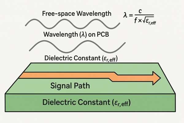
Calculating Wavelength: The Substrate's Impact
The most important factor in this calculation is the material your PCB is made from, which determines the signal's propagation speed.
Understanding Effective Dielectric Constant (\(\epsilon_{r,eff}\))
For a trace buried inside the PCB (stripline), the signal is surrounded by the substrate, so the effective dielectric constant is the same as the material's \(\epsilon_{r}\). But for a trace on an outer layer (microstrip), the field is in both the substrate and the air above it. This lowers the effective dielectric constant. For FR-4, with a bulk \(\epsilon_{r}\) of \(\approx 4.2\), the \(\epsilon_{r,eff}\) for a microstrip is often closer to \(\approx 3.2\).
Beyond Dielectric Constant: The Impact of Loss Tangent (\(\tan\delta\))
At frequencies above 1 GHz, another material property becomes critical: the loss tangent (\(\tan\delta\))4, or dissipation factor. This measures how much of the signal's energy is absorbed and converted to heat by the dielectric. A material like standard FR-4 has a high loss tangent (e.g., 0.02), which severely attenuates multi-gigahertz signals. High-performance materials like Rogers RO4350B5 have a much lower loss tangent (e.g., 0.0037), preserving signal amplitude. While not directly causing radiation, high loss requires more powerful drivers, which can lead to other EMI issues.
| Material | \(\epsilon_{r}\) @ 10GHz | \(\tan\delta\) @ 10GHz | Signal Integrity |
|---|---|---|---|
| Standard FR-4 | \(\approx 4.1\) | \(\approx 0.020\) | Poor for \(> 3-5 \text{ GHz}\) |
| High-Performance FR-4 | \(\approx 3.7\) | \(\approx 0.012\) | Good for 5-10 GHz |
| Rogers RO4350B | \(\approx 3.48\) | \(\approx 0.0037\) | Excellent for \(> 10 \text{ GHz}\) |
What is a "Critical Length" for a PCB Trace?
When does a simple trace become a complex transmission line? There's a specific threshold known as the "critical length." Exceeding this length without proper design considerations, like controlled impedance, will lead to signal integrity problems like reflections and distortion.
The critical length is the maximum trace length beyond which it must be treated as a transmission line. A common rule of thumb defines this length as the distance a signal travels in half of its rise time. For digital signals, the formula is: \(L_{crit} = \frac{t_{r}}{2 \times t_{pd}}\), where \(t_{r}\) is the signal rise time and \(t_{pd}\) is the propagation delay per unit length.
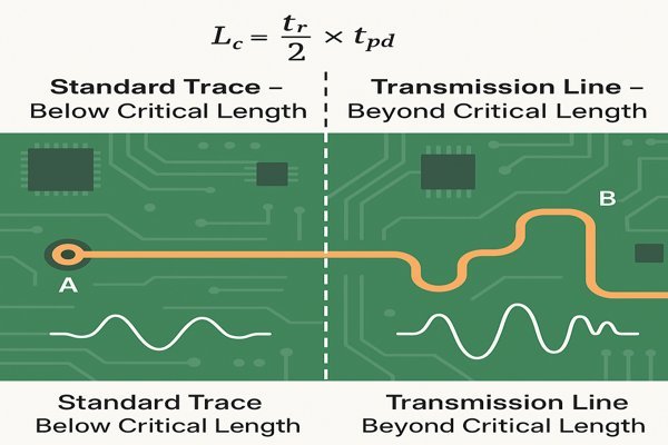
When a Trace Becomes a Transmission Line
This concept is all about preventing signal reflections from corrupting your data. On short traces, reflections return to the source so quickly they don't cause a problem. On long traces, they arrive late and cause distortion.
The Role of Signal Rise Time6
The faster the signal's rise/fall time (\(t_{r}\)), the shorter the critical length becomes. The rise time, not the clock frequency, is what truly defines a signal as "high-speed." The propagation delay (\(t_{pd}\)) on FR-4 is typically around \(150-180 \text{ ps/inch}\).
| Signal Rise Time (\(t_{r}\)) | Logic Family Example | Propagation Delay7 (\(t_{pd}\)) | Calculated Critical Length |
|---|---|---|---|
| 5 ns | Older TTL/CMOS | \(160 \text{ ps/inch}\) | ~9.8 inches (~24.9 cm) |
| 1 ns | LVCMOS, DDR2 | \(160 \text{ ps/inch}\) | ~3.1 inches (~7.9 cm) |
| 200 ps | DDR4, PCIe Gen 3 | \(160 \text{ ps/inch}\) | ~0.6 inches (~1.5 cm) |
| 50 ps | PCIe Gen 5, 100GbE | \(160 \text{ ps/inch}\) | ~0.15 inches (~3.9 mm) |
According to established high-speed design guidelines, any trace approaching these lengths must have its impedance controlled to ensure signal integrity.
What Are Methods to Prevent PCB Traces from Acting as Antennas?
Facing EMI issues from radiating traces? The solution isn't just one thing, but a combination of good design practices. You can significantly reduce unintentional radiation by controlling trace geometry, ensuring solid ground references, and using proper layout techniques from the start.
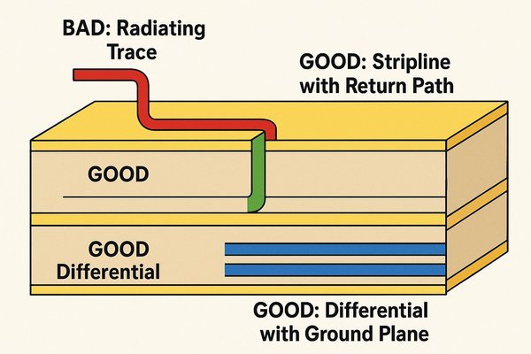
Key methods include keeping high-speed traces as short as possible, providing a continuous, low-impedance ground return path directly beneath the trace, using differential signaling, avoiding sharp 90-degree bends, and burying critical traces between ground planes (stripline).
Practical Layout Strategies to Minimize Radiation
The most effective way to prevent a trace from radiating is to minimize the area of its current loop. The loop is formed by the signal trace and its return path in the ground plane.
1. Minimize the Current Loop Area
A large loop acts like a very effective magnetic loop antenna. Any break or split in the ground plane under a trace forces the return current to detour, massively increasing the loop area and EMI radiation. This is why an unbroken ground plane is the golden rule of high-speed design.
2. Use 45-Degree Bends
While the idea that 90-degree bends "radiate" is sometimes overstated, the real issue is that a sharp corner creates an impedance discontinuity. The trace is wider at the corner, causing a local drop in impedance that leads to reflections. These reflections can create standing waves and contribute to EMI. Using two 45-degree bends maintains a more consistent trace width and impedance.
3. Use Differential Signaling
For high-speed interfaces like USB, Ethernet, and PCIe, differential signaling is standard practice for a reason. By sending the signal down two tightly coupled traces with opposite polarity (+ and -), the electromagnetic fields they generate are equal and opposite. In the far-field, these fields cancel each other out, drastically reducing EMI. This also provides excellent immunity to incoming noise.
What are Shielding and Grounding Techniques for Reducing EMI on a PCB?
Need to protect your sensitive circuits from noise? Effective shielding and grounding are your first line of defense. These techniques work by either containing electromagnetic fields at their source or providing a low-impedance path to divert noise away from critical components.
Key techniques include using solid ground planes, employing via stitching to connect ground areas, adding shielding cans over noisy components, using guard traces around sensitive signals, and ensuring proper chassis grounding. A solid ground plane is the most fundamental and effective EMI shield on a PCB.
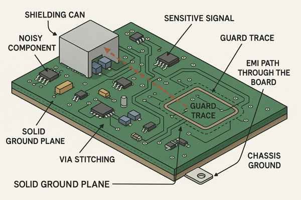
Building a Fortress: Grounding and Shielding for EMI
A good grounding and shielding strategy creates controlled zones on the PCB, preventing noisy circuits from interfering with sensitive ones.
The Power of the Ground Plane
A solid ground plane provides a universal low-impedance return path for signals and acts as a shield. But its effectiveness depends on its integrity. Every via that punches through it creates a hole, and too many holes can turn a solid plane into a "Swiss cheese" plane, increasing its impedance and reducing its shielding effectiveness.
The Power Distribution Network (PDN)8 as an EMI Source
High-speed ICs draw current in sharp, fast bursts. This high-frequency noise can turn your power planes into radiating antennas if not managed. A robust PDN design is crucial for EMI control. This involves placing decoupling capacitors9 as close as possible to every power pin on an IC. These caps provide a local, low-impedance source for high-frequency current, preventing noise from propagating across the power planes. Using low-inductance (low-\(\text{ESL}\)) capacitors is critical for this to be effective at high frequencies.
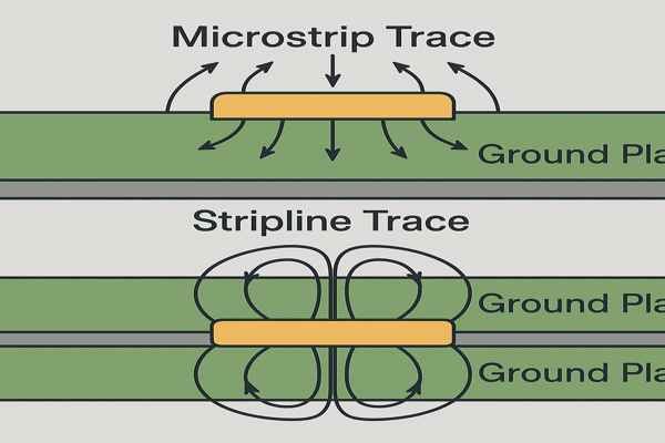
What is the Difference Between a Microstrip and a Stripline, and How Does Each Affect Radiation?
Choosing where to route your high-speed traces is a major decision. The choice between a microstrip (outer layer) and a stripline (inner layer) configuration has significant consequences for signal integrity, impedance control, and especially EMI radiation.
A stripline trace, buried between two ground planes, contains its fields and radiates very little. A microstrip, on an outer layer with one ground plane, has an open structure that allows its fields to radiate easily, making it a greater EMI risk.
Microstrip vs. Stripline: Choosing Your Routing Strategy
The choice between these two routing topologies is a classic engineering trade-off between performance and cost.
The Contained World of Stripline
A stripline configuration is like a flattened coaxial cable. The two reference planes above and below the trace confine the electromagnetic fields, drastically reducing EMI and crosstalk. As such, PCB fabricators and high-speed design experts recommend stripline for the most critical signals like system clocks.
An Alternative: Coplanar Waveguide10 (CPW)
For RF or very high-speed signals on an outer layer, a Coplanar Waveguide offers a good compromise. It consists of the signal trace flanked by ground planes on the same layer, with the ground areas stitched by vias to the main ground plane below. This provides good field containment without the cost of extra layers needed for stripline, but requires more surface area.
| Feature | Microstrip | Stripline | Coplanar Waveguide (Grounded) |
|---|---|---|---|
| EMI Radiation | High | Very Low | Low-to-Medium |
| Cost | Lowest | Highest | Medium |
| Layer Count | Minimum 2 | Minimum 4 | Minimum 2 |
| Debugging | Easiest | Impossible | Easy |
What are the Design Principles for Achieving Good Signal Integrity at High Frequencies?
Want your high-speed digital circuits to work reliably? Good signal integrity (SI) is not an accident; it's the result of deliberate design choices. It involves preserving the signal's shape and timing as it travels from the driver to the receiver, fighting against noise, reflections, and distortion.
The core principles are: maintaining continuous controlled impedance, providing a solid, uninterrupted ground return path, minimizing trace length, using proper termination schemes to prevent reflections, and managing crosstalk between adjacent signals by ensuring adequate spacing.
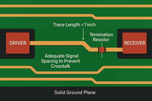
The Foundations of High-Speed Design
Good signal integrity ensures that a '1' looks like a '1' and a '0' looks like a '0' when the signal arrives at its destination. This requires managing several key electrical phenomena.
Managing Via Transitions
When a high-speed signal travels through a via to another layer, it encounters a significant impedance discontinuity. The via is a cylindrical barrel, not a flat trace, and it disrupts the return current path. This can cause severe reflections. For multi-gigahertz signals, this is critical. The solution is to place ground stitching vias immediately adjacent to the signal via. This provides a short, direct path for the return current to follow the signal from one reference plane to another, minimizing the discontinuity. For very high-speed buses like PCIe 4.0/5.0, via impedance must be carefully modeled and controlled.
Linking Problems to Solutions
| SI Problem | Primary Cause(s) | Design Solution(s) |
|---|---|---|
| Ringing/Overshoot | Impedance mismatch, improper termination | Controlled impedance traces, add termination resistor. |
| Crosstalk11 | Fields coupling between adjacent traces | Increase trace spacing (3W rule), use stripline routing. |
| Via Discontinuity | Broken return path, via capacitance/inductance | Add adjacent ground stitching vias, optimize via size. |
What Tools Are Available for Simulating EMI and Signal Integrity in PCB Designs?
How can you be sure your design will work before spending thousands on prototypes? Simulation is the answer. Modern EDA software includes powerful tools that allow you to analyze your PCB for signal integrity issues and predict its EMI performance before you ever send it to fabrication.
Leading tools for SI and EMI simulation include Keysight's ADS, Ansys's SIwave and HFSS, Cadence's Sigrity, and integrated toolsets within EDA platforms like Altium Designer and Zuken's CR-8000. These tools use field solvers to model the electromagnetic behavior of your PCB layout.

Simulate Before You Fabricate: Modern EDA Tools
These simulation tools are no longer a luxury; for high-speed design, they are a necessity. They provide insight that is impossible to get from simple design rule checks.
A Practical Simulation Workflow
Instead of just checking at the end, simulation should be integrated throughout the design process:
- Pre-Layout Simulation: Before routing, use tools to experiment with different layer stack-ups, trace widths, and termination strategies. This helps you define the design rules for your board.
- Post-Layout Verification: After routing is complete, extract the actual routed traces and run SI simulations on critical nets (e.g., DDR buses). This verifies that the real-world layout meets timing and quality margins, checking for issues like reflections and crosstalk.
- Full-Board EMI/EMC Simulation: As a final step, use a 3D full-wave solver like Ansys HFSS to analyze the entire board for radiated emissions. This can identify unexpected "hot spots"—like inadequately shielded connectors or resonant slots in a ground plane—before you commit to expensive fabrication and lab testing.
Conclusion
Ultimately, preventing PCB traces from acting as antennas boils down to controlling the electromagnetic fields. By understanding signal harmonics, managing return paths, choosing the right materials and routing strategies, and simulating your design, you can engineer reliable, compliant products and avoid costly EMI failures.
-
Explore IPC-2251 to understand industry standards for PCB design and how they impact signal integrity and transmission lines. ↩
-
Understanding harmonics is crucial for effective PCB design, especially for high-speed signals and minimizing EMI. ↩
-
Understanding the monopole antenna is crucial for grasping antenna design and resonance principles. ↩
-
Understanding loss tangent is crucial for selecting materials that minimize signal loss and improve performance in high-frequency applications. ↩
-
Rogers RO4350B is known for its excellent performance at high frequencies, making it a top choice for advanced PCB applications. ↩
-
Understanding Signal Rise Time is crucial for maintaining signal integrity in high-speed designs. Explore this link to deepen your knowledge. ↩
-
Propagation Delay is a key factor in circuit design that influences performance. Learn more about its impact on signal integrity. ↩
-
Learn about the critical role of PDN in managing EMI, which is vital for high-speed IC performance. This resource will deepen your understanding. ↩
-
Understanding decoupling capacitors is essential for effective EMI control in high-speed circuits. Explore this link to enhance your knowledge. ↩
-
Explore this link to understand how Coplanar Waveguide can optimize your RF and high-speed signal routing effectively. ↩
-
Learning about crosstalk is crucial for any designer aiming to improve signal integrity and reduce interference in high-speed circuits. ↩


