 Skip to content
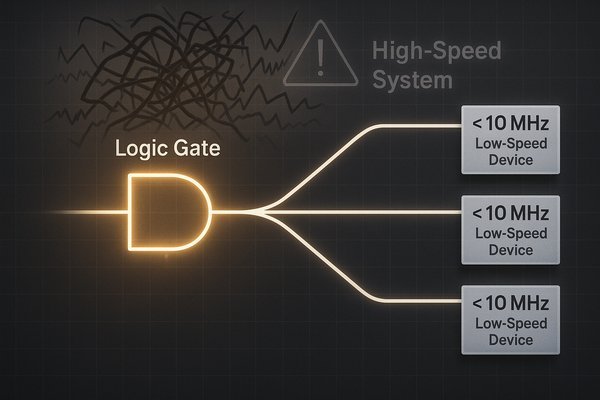
Struggling to route a clock signal with limited components? Using a spare logic gate seems clever, but this shortcut can introduce critical timing failures that are a nightmare to debug.
Yes, a logic gate can substitute for a clock buffer in very low-speed (<10 MHz), non-critical applications where timing is loose. However, for any synchronous or high-speed system, a dedicated clock buffer is essential for its controlled impedance, low skew, and minimal jitter that logic gates can't provide.
I've seen this shortcut attempted in early-stage prototypes, and while it's tempting, the potential for instability is huge. The problem isn't just about delay; it's about uncertainty and signal quality. A standard logic gate's primary job is to perform a logical function, not to preserve the integrity of a timing signal. I once spent days debugging a system where a designer used a spare NAND gate as a clock inverter. The slow, asymmetrical fall time was causing intermittent failures at higher temperatures. Replacing it with a proper clock buffer, which has a controlled slew rate and specified low skew, solved the issue instantly.
Logic Gate vs. Clock Buffer: Key Differences
| Specification | Standard Logic Gate (e.g., 74LVC series) | Dedicated Clock Buffer |
|---|---|---|
| Propagation Delay (\(t_{pd}\)) | Highly variable (e.g., 1 ns to 6.5 ns) over PVT. | Tightly controlled and specified. |
| Output Skew | Not a specified parameter; can be very high. | Very low (e.g., 15-50 ps); a primary performance metric. |
| Slew Rate (Rise/Fall) | Slow, often asymmetrical, not controlled. | Fast, controlled, and symmetrical to ensure clean edges. |
| Drive Strength | Low; not designed for 50Ω transmission lines. | High; designed to drive multiple 50Ω terminated lines. |
| Ideal Use Case | Performing logical operations. | Distributing a high-integrity clock signal. |
Can an FPGA's Internal Clock Manager Be Used Instead of an External Clock Buffer?
Your FPGA has powerful internal clocking resources, so why add an external buffer? Because relying only on the FPGA can limit drive strength and risk signal integrity for off-chip components.
An FPGA's internal clock manager (e.g., a Xilinx MMCM or Intel PLL) is perfect for generating and distributing clocks inside the FPGA. For driving multiple external chips, an external clock buffer provides superior off-chip drive strength, signal integrity, and controlled fan-out.
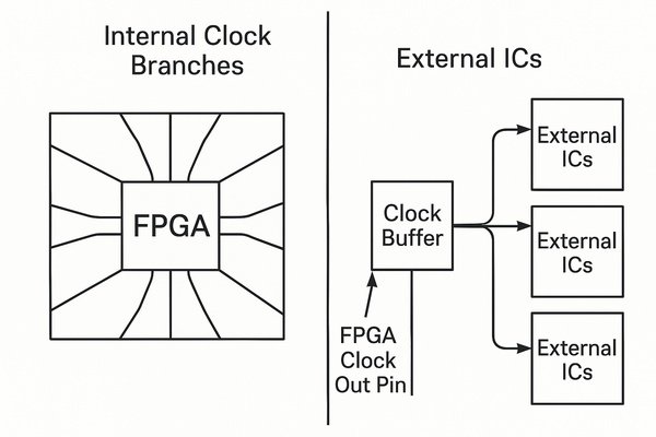
In my experience, the core issue is impedance mismatch and noise. An FPGA's general-purpose I/O pins are not inherently designed to drive a controlled 50Ω transmission line to multiple destinations. While you can select I/O standards like HSTL or LVDS, these consume more power and require specific termination schemes. A dedicated clock buffer, on the other hand, has outputs specifically engineered to drive 50Ω loads with minimal reflections.
Another critical factor is noise isolation. If your clock output pin is in the same I/O bank as a wide data bus, the simultaneous switching of that bus can induce significant noise (Simultaneous Switching Output, or SSO noise) onto your clock signal. This adds jitter that can violate timing on your external components. An external buffer acts as a barrier, taking the potentially noisy clock from the FPGA, cleaning it up with its stable power supply, and re-driving clean copies to the rest of the system. Sometimes, a $2 external buffer is a more cost-effective solution than upgrading to a larger FPGA just for better clocking resources.
Internal vs. External Clock Distribution
| Feature | FPGA Internal Clock Manager (e.g., MMCM/PLL) | External Clock Buffer |
|---|---|---|
| Primary Use Case | On-chip clock synthesis and distribution. | Off-chip clock fan-out and signal conditioning. |
| Off-Chip Drive | Limited; requires careful I/O standard selection and termination. | High; designed to drive multiple 50Ω loads. |
| Off-Chip Skew | Higher; affected by I/O buffer variation and routing. | Very low; specified output-to-output skew (e.g., 15-50 ps). |
| Noise Immunity | Susceptible to on-chip noise (e.g., SSO). | Isolates external clock tree from FPGA noise. |
| FPGA Resources | Consumes internal CMT/PLL and GCLK routing. | Zero FPGA resource usage. |
What Is the Difference Between a Clock Buffer and a PLL (Phase-Locked Loop)?
Clock buffers and PLLs both manage timing signals, which can be confusing. But picking the wrong one means your system either has a noisy clock or is over-engineered, wasting money.
A clock buffer simply distributes a clock; it takes one input and creates multiple, identical copies. A PLL (Phase-Locked Loop) is a feedback system that generates new frequencies, multiplies/divides clocks, or actively cleans jitter from a noisy input clock.

The key distinction is that a buffer is a passive distributor, while a PLL is an active modifier. The "jitter cleaning" ability of a PLL is one of its most powerful features. It works because the internal loop filter acts as a low-pass filter for phase variations. High-frequency jitter on the input reference clock is effectively averaged out, and the Voltage-Controlled Oscillator (VCO) only tracks the slow, long-term frequency. This results in an output clock that has the same average frequency but significantly less jitter.
A classic application for this is in systems with recovered clocks, like from a SerDes (Serializer/Deserializer) in a fiber optic link. The clock recovered from the incoming data stream can be quite jittery due to noise and signal degradation in the transmission medium. Before using this clock to drive logic in the receiving system, we almost always pass it through a dedicated jitter-attenuating PLL. This cleans the clock, re-establishes a solid timing reference, and prevents bit errors in the downstream processing.
Clock Buffer vs. PLL at a Glance
| Aspect | Clock Buffer (Fan-out Buffer) | PLL (Phase-Locked Loop) |
|---|---|---|
| Core Function | Distribute (fan-out) a single clock signal. | Generate, multiply/divide, or clean a clock signal. |
| Input vs. Output | Output frequency = Input frequency. | Output frequency can be a multiple/division of the input. |
| Jitter | Adds a small amount of jitter (additive jitter). | Can significantly reduce (clean) input jitter. |
| Complexity | Simple, feed-forward digital logic. | Complex analog/digital feedback loop system. |
| When to Use | When you need to send one clock to many devices. | When you need to create a new frequency or de-jitter a noisy clock. |
When Should a Clock Generator IC Be Used Instead of a Clock Buffer?
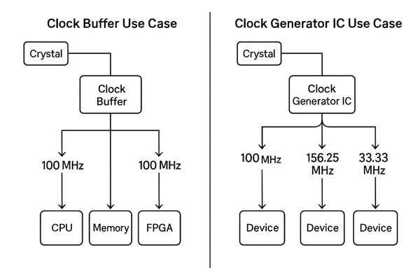
Your system needs multiple clock frequencies for different interfaces. Using several crystals and oscillators eats board space, increases BOM cost, and creates potential synchronization issues between clock domains.
Use a clock buffer when you need to distribute a single clock frequency to multiple places. Use a clock generator IC when you need to create multiple different clock frequencies (e.g., 100 MHz, 156.25 MHz, 33.33 MHz) from a single reference crystal.
Modern clock generators are incredibly versatile. They don't just consolidate your clock sources; they provide flexibility that is invaluable during development and production. Many are programmable via an I²C or SPI interface, allowing you to change clock frequencies on the fly without any hardware changes. On one medical device project, this feature was a lifesaver. We needed to validate the performance of our ADC with different sampling rates. Instead of building multiple prototype boards, we simply wrote to a register in our clock generator to change the ADC clock from 100 MHz to 125 MHz, which saved weeks of hardware spins.
Furthermore, these generators often provide multiple output banks that support different signaling standards like LVCMOS, LVDS, LVPECL, or HCSL from a single chip. This is incredibly useful in mixed-signal systems where a processor might need a 1.8V LVCMOS clock, while a high-speed SerDes needs a 100 MHz differential HCSL clock for a PCIe link. Trying to create these with separate oscillators and level-shifters would be a complex and space-consuming mess.
Choosing the Right Clocking Component
| Component | Input | Output | Primary Role & Features |
|---|---|---|---|
| Clock Buffer | 1 clock frequency | Multiple copies of the same frequency | Distribution / Fan-out |
| Clock Generator | 1 reference (e.g., crystal) | Multiple, different clock frequencies | Synthesis / Consolidation. Often programmable and multi-standard. |
| PLL | 1 clock frequency | 1 (or more) frequency, often modified | Generation / Jitter Cleaning |
| Oscillator (XO) | DC Power | 1 fixed clock frequency | Source / Origination |
How Is a Clock Buffer's Performance Factored Into a System's Overall Timing Budget?
You've passed your timing simulations, but the prototype hardware has intermittent data errors. An often-overlooked component, the clock buffer, could be the silent thief eating your timing margin.
A clock buffer’s key parameters—propagation delay, output-to-output skew, and additive jitter—are directly subtracted from your total system timing budget. These specifications reduce the available data valid window, shrinking the setup and hold time margins for all connected ICs.
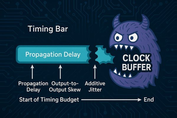
When I'm doing a timing analysis, I treat the clock buffer as a source of unavoidable error that must be accounted for. The table below defines the key parameters from a buffer's datasheet and how they impact your design.
Key Clock Buffer Timing Parameters
| Parameter | Symbol | Definition | Impact on Timing Budget |
|---|---|---|---|
| Propagation Delay | \(t_{pd}\) | Time from input edge to corresponding output edge. | The variation (min/max) affects both setup and hold calculations. |
| Output-to-Output Skew | \(t_{sk(o)}\) | Max difference in \(t_{pd}\) between all outputs. | Directly subtracts from the timing margin for setup time. |
| Additive Jitter | \(t_{j(add)}\) | RMS jitter added by the buffer itself. | Increases the total system jitter, shrinking the valid data window. |
| Period Jitter | \(J_{\text{per}}\) | Max deviation of any single clock period from the ideal. | Critical for sampling systems like ADCs/DACs. |
Let's walk through a setup time calculation with a practical example. Assume we have a 100 MHz clock (10 ns period) driving a system.
\(\text{Setup Margin} = T_{\text{period}} - T_{co,max} - T_{data,max} - T_{su} - T_{jitter} - T_{skew}\)Let's plug in some numbers:
- Clock Period: 10 ns
- Source IC Clock-to-Out (\(T_{co}\)): 2.0 ns
- Data Path Delay (\(T_{data}\)): 4.0 ns
- Destination IC Setup Time (\(T_{su}\)): 1.0 ns
- Total Jitter (\(T_{jitter}\)): 250 ps
- Buffer Skew (\(T_{skew}\)): 150 ps
\(\text{Initial Margin} = 10 \text{ ns} - 2.0 \text{ ns} - 4.0 \text{ ns} - 1.0 \text{ ns} = 3.0 \text{ ns}\)
\(\text{Final Margin} = 3.0 \text{ ns} - 0.25 \text{ ns} - 0.15 \text{ ns} = 2.6 \text{ ns}\)
The buffer's imperfections consumed 400 ps, or 13%, of our initial timing margin. This shows how quickly these small numbers add up to make a real difference.
Conclusion
Choosing the right clocking component is vital. A logic gate is a risky shortcut, while dedicated buffers, generators, and PLLs provide the precision and reliability essential for stable high-speed designs.


