 Skip to content
Struggling with manufacturing delays caused by poor component placement? You're not alone. Inefficient orientation can lead to assembly line jams, soldering defects, and costly rework, derailing your entire project schedule.
The orientation of components directly impacts manufacturing speed and reliability. Consistent alignment reduces pick-and-place machine travel time, prevents soldering defects like shadowing in wave soldering, and simplifies automated optical inspection (AOI), leading to higher yields and lower assembly costs.
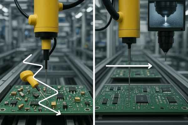
I've seen firsthand how a seemingly minor layout choice can create major production headaches. A well-thought-out component placement strategy is fundamental to Design for Manufacturability (DFM). It’s not just about making the circuit work; it’s about making it buildable, reliably and at scale. I once worked on a project where the components were placed at various angles to make routing seem easier. The pick-and-place machine's rotational head was constantly working overtime, slowing the assembly time per board from a projected 45 seconds to over 70 seconds. On a run of 10,000 units, that inefficiency added weeks to the delivery schedule and thousands of dollars in assembly costs. This guide breaks down the critical rules to help you avoid these costly mistakes.
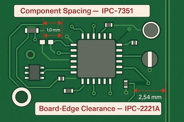
What Are the IPC Standards for Component Spacing and Board-Edge Clearances?
Frustrated by assembly failures due to components being too close? This common issue can cause shorts, prevent proper soldering, and make rework nearly impossible, leading to costly board scrap.
IPC standards provide minimum spacing rules to ensure manufacturability and reliability. For example, IPC-7351 suggests component-to-component spacing based on density levels, while IPC-2221A recommends a minimum of 2.54 mm (0.100 inches) clearance from component to board edge to avoid damage during depanelization and handling.
Understanding these standards is non-negotiable for any hardware engineer. They are the baseline for a successful product. In my experience, especially on high-volume projects like the Tuxedo Keypad at Honeywell, adhering to these rules from the start saved us from countless manufacturing spins.
Understanding Courtyard Density Levels
The IPC-73511 standard defines three density levels for component courtyards. This choice has direct cost and yield implications. "Most" density, while great for miniaturization, requires your fabricator to hold tighter tolerances, which can increase the base PCB cost. It also drastically reduces the process window for automated assembly, potentially lowering yield. "Least" density is safest and cheapest from a yield perspective but may force you into a larger, more expensive PCB or require more layers. I always start a design with "Nominal" (Level B) density. I only push to "Most" (Level A) for specific areas, like under a BGA, and I always flag this in my design notes for the contract manufacturer (CM). This proactive communication prevents them from making assumptions that could lead to assembly issues.
Practical Implications of Board Edge Clearance
The 2.54 mm (100 mil) keep-out rule from IPC-2221A2 is a lifesaver. This clearance isn't just for the router bit; it’s also for the tooling pins and clamps that hold the PCB panel flat during solder paste screening and assembly. If a component is in this zone, the CM can't secure the board properly, leading to inconsistent solder paste deposits—a primary cause of defects. With V-grooves, the mechanical stress during depanelization is significant. I’ve seen ceramic capacitors, which are brittle, develop micro-fractures when placed too close to a V-groove. These fractures can pass initial testing but fail months later in the field, leading to costly warranty returns. It’s a silent killer, and respecting edge clearance is the cure.
Here is a more structured breakdown of key clearance requirements based on IPC standards:
| Clearance Type | IPC Standard | Recommended Minimum Value | Why It Matters |
|---|---|---|---|
| Component-to-Component | IPC-7351 | Varies by density level: Least: 0.25mm (10 mils), Nominal: 0.50mm (20 mils), Most: 1.00mm (40 mils) courtyard excess. | Prevents solder bridging, allows for rework access, and ensures automated placement accuracy. |
| Component-to-Board Edge (Routed) | IPC-2221A | 2.54 mm (0.100 inches) | Protects components from mechanical stress during depanelization and handling. |
| Component-to-Board Edge (V-Groove) | IPC-2221A | 1.27 mm (0.050 inches) away from the center of the V-groove. | Prevents component damage when the boards are snapped apart. |
| Copper-to-Board Edge | IPC-2221A | 0.5 mm (0.020 inches) for external layers. | Prevents shorting and damage to copper features during routing or cutting. |
| Mounting Hole-to-Board Edge | IPC-2221A | 3.175 mm (0.125 inches) | Ensures mechanical stability and prevents cracking around the mounting holes. |
Note: These values are general guidelines. Always consult the latest IPC documentation and your manufacturer's capabilities for specific applications.
What Placement Rules Are Critical When Designing for Wave Versus Reflow Soldering?
Are your wave-soldered boards failing inspection? The wrong component layout can cause solder skips or bridges, as taller components can "shadow" smaller ones from the solder wave, ruining entire batches.
For wave soldering, orient similar components in the same direction and place smaller parts so they precede larger ones into the wave. For multi-pin ICs, align the longest axis parallel to the direction of wave travel to prevent solder bridging between pins.
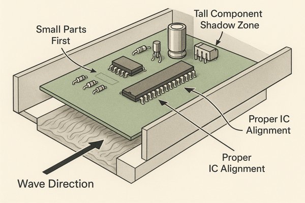
The physics of the soldering process dictates these rules. Wave soldering is a top-down process where the board passes over a molten wave of solder. Any component that obstructs this flow can create defects.
The Physics of Solder Shadowing
Solder shadowing is a real, physical phenomenon. To combat it, you need to think like a fluid dynamics engineer. The rule of thumb for clearance behind a tall component is based on the angle of the solder wave, typically around 10-15 degrees. This is why a taller component casts a longer "shadow." For a 10mm tall capacitor, this can create a "dead zone" of 30-50mm behind it where solder flow is turbulent or non-existent. Another critical point is component selection. Some packages are simply incompatible with wave soldering. For example, QFNs or BGAs with pads on the bottom of the package cannot be wave soldered because there's no way for the solder to reach the pads. If you have a mixed-technology board, these components must be on the top side for reflow.
Designing Solder Thieves and Preventing Tombstoning
To prevent bridging on fine-pitch components during wave soldering, we use "solder thieves." This is simply an extra, non-functional pad placed at the trailing edge of a row of pins. Its purpose is to wick away excess solder that would otherwise form a bridge on the last pin. A good thief pad is typically the same size as a component pad or slightly larger. For reflow, the primary enemy is tombstoning3. I’ve seen this happen most often with 0402 and smaller passives. The key preventative measure, besides symmetrical pads, is designing robust thermal reliefs for pads connected to large copper planes. A typical thermal relief uses two or four 0.25mm (10 mil) spokes to connect the pad to the plane. This restricts heat flow just enough to ensure both pads reflow simultaneously without compromising the electrical connection.
Here’s a comparison of key placement rules:
| Design Consideration | Wave Soldering | Reflow Soldering |
|---|---|---|
| Component Orientation | Critical. Align ICs parallel to the wave. Orient SOTs and other small discretes perpendicular to the wave to ensure both pads are soldered evenly. | Less critical but important. Symmetrical pad design and balanced thermal mass are key to preventing tombstoning. |
| Component Shadowing | Major issue. Place shorter components in front of taller components relative to the wave direction. Leave ample space (e.g., > 5 mm) behind tall parts. | Not an issue. Heat is applied uniformly from above, so shadowing does not occur. |
| Component Spacing | Must be generous to allow solder to flow freely. Solder thieves (extra pads) are often needed at the trailing edge of fine-pitch components. | Can be denser, limited primarily by pick-and-place and rework needs. |
| Adhesive Application | Required for bottom-side SMT components to hold them in place as they pass through the solder wave. | Not required, as solder paste holds components in place before and during reflow. |
What Are the Design Tradeoffs for Double-Sided Component Placement?
Considering a double-sided design to save space? While it increases density, it also doubles the assembly steps and can introduce new thermal and mechanical challenges, potentially driving up costs and complexity.
The primary benefit of double-sided placement is a ~50% reduction in board area. However, this comes at the cost of an additional reflow or wave soldering cycle, increased handling complexity, and potential thermal issues if heat-sensitive components are placed opposite high-power parts.
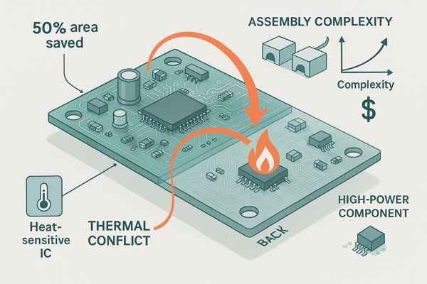
At Lightelligence, I worked on an extremely dense evaluation board for a photonic chip where double-sided placement was unavoidable. The challenge was managing the thermal profile and assembly complexity.
Cost and Fixturing Analysis
The cost of double-sided assembly isn't just the second run through the SMT line. For the second side, the board, now populated on top, cannot lie flat on the conveyor. It must be placed in a custom-machined carrier pallet or fixture. These pallets are a non-recurring engineering (NRE) charge4 that can range from $500 to $3,000+ depending on complexity. This NRE cost must be factored into your decision. The breakeven point often comes when the savings from a smaller PCB (and potentially a smaller product enclosure) outweigh this fixturing cost over the lifetime volume of the product. Also, remember that every extra process step is another opportunity for failure, so double-sided designs inherently have a slightly lower first-pass yield.
The Rework Nightmare
Reworking a dense, double-sided board is a technician's worst nightmare and a major cost driver. Imagine trying to use a hot air gun to replace a QFP on the top side. Without proper shielding, the heat will conduct through the board and reflow the solder on components directly underneath, causing them to shift or fall off. Specialized rework stations5 use bottom-side preheaters and precisely focused nozzles to mitigate this, but it's a slow, highly skilled process. As a designer, you can make this easier by not placing small, lightweight passives on the bottom side directly opposite large, high-pin-count packages on the top side. This small consideration can save hours of rework time.
Here’s a breakdown of the key tradeoffs:
| Factor | Pro: Advantages of Double-Sided Placement | Con: Disadvantages of Double-Sided Placement |
|---|---|---|
| Board Size & Cost | Significantly reduces PCB footprint, which can lower the raw board cost and allow for smaller product enclosures. | Increases assembly costs due to a second pass and NRE for fixtures ($500+). Overall product cost might increase. |
| Component Density | Maximizes use of board real estate, enabling more complex circuits in a smaller form factor. | Can make routing very challenging. May require more layers or microvias, increasing PCB fabrication cost. |
| Thermal Management | Can help isolate high-power components from sensitive analog circuits by placing them on opposite sides. | Components on the bottom side can be heated during the second reflow cycle, potentially damaging them if they are heat-sensitive. |
| Assembly & Rework | N/A | Complex assembly setup. Rework is much more difficult, as heating one side can affect components on the other. Requires careful support fixtures. |
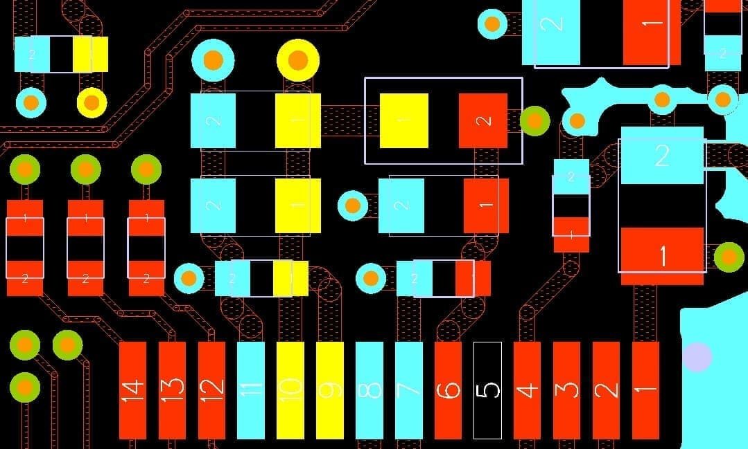
What Is the Recommended Placement for Components Near Their Associated Vias?
Placing vias too far from their component pads? This can introduce unwanted inductance and resistance, degrading high-speed signal integrity and creating power delivery issues that are a nightmare to debug.
For optimal performance, especially in high-speed or high-current designs, place vias as close as possible to the component pad. For decoupling capacitors, the via connecting to the ground plane should be placed immediately adjacent to the capacitor's ground pad to minimize loop inductance.
This is a lesson I learned the hard way. On an early FPGA project, we were seeing intermittent data corruption on a high-speed memory bus. The cause was excessive inductance in the power distribution network (PDN).
The Impact of Via Placement on PDN Impedance
Every millimeter of trace between a capacitor pad and its via adds parasitic inductance, estimated at roughly 0.5 nH/mm. This seems tiny, but in a fast-switching digital circuit where current changes in nanoseconds (\(\frac{di}{dt}\)), this inductance creates significant voltage droop (\(V = L \cdot \frac{di}{dt}\)). Placing the ground via immediately next to the capacitor's ground pad, and the power via next to the power pad, creates the smallest possible current loop. This simple, free layout choice is your first and best line of defense for maintaining a low-impedance PDN and ensuring your high-speed chips have stable power.
Thermal Benefits of Vias
Vias aren't just for electrical signals; they are also excellent thermal conductors. For any component with a thermal pad (like a QFN or a power MOSFET), placing an array of thermal vias directly in or under the pad is a critical and low-cost way to transfer heat to inner ground or power planes, which then act as heatsinks. A typical thermal via might have a 0.3mm drill hole and a 0.6mm pad. A 3x3 or 4x4 grid of these under a thermal pad can lower the component's thermal resistance (Rth) by 10-30%. This can be the difference between a component running reliably and one that overheats and fails prematurely. It’s one of the most effective thermal management techniques available to a PCB designer.
| Via Placement Strategy | Description | Pros | Cons | Best For |
|---|---|---|---|---|
| Via Next to Pad | The standard approach. A short trace connects the SMT pad to a via placed just outside the pad. | Low-cost, easy to fabricate. | Adds trace length, increasing inductance and resistance. Consumes more board space. | General-purpose, non-critical signals. |
| Via in Pad (Filled & Capped) | The via is drilled directly inside the SMT pad and then filled with conductive or non-conductive epoxy and plated over. | Lowest possible inductance. Improves thermal dissipation. Frees up routing channels. | Higher fabrication cost (10-20%+). Requires specialized manufacturing processes. | High-speed signals (e.g., >1 GHz), BGA breakout, high-power components. |
| Dog Bone | A short trace connects the via to the pad, resembling a bone shape. Commonly used for BGA breakout. | Good compromise between cost and performance. Better than a long trace. | Still has more inductance than via-in-pad6. The fanout pattern can consume significant routing space under the BGA. | BGA packages with pitches > 0.8mm. |
| Microvia (in Pad) | A laser-drilled via with a very small diameter (typically < 0.15mm) placed directly in the pad. | Excellent for high-density interconnect (HDI) boards. Very low inductance. | Limited to connecting only the outer layer to the next layer. Expensive fabrication. | HDI designs, fine-pitch BGAs (< 0.5mm), mobile devices. |
What Is the Best Strategy for Placing Test Points for Manufacturing Tests and Debugging?
Have you ever designed a board that was impossible to test or debug? Without accessible test points, you're flying blind, making failure analysis a painful and time-consuming process for both you and the manufacturer.
The best strategy is to place all test points on one side of the PCB (typically the bottom), maintain a minimum center-to-center spacing of 1.27mm (0.050 inches), and ensure they are at least 2.54mm (0.100 inches) from the board edge and tall components.
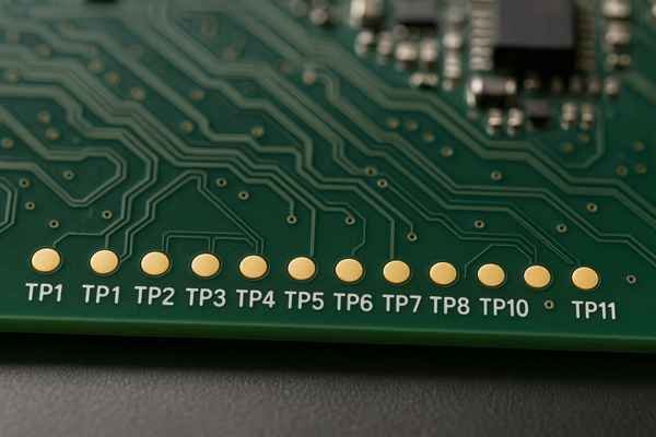
A solid test point strategy is a core part of Design for Test (DFT). At Smiths Medical, where reliability is paramount, every critical net on the infusion pump hardware had a dedicated test point.
Test Points: Pad, Via, or Component?
You have three options for creating a test point: using an exposed pad (often a dedicated SMD pad with no paste), an exposed via (often called a "test via"), or a dedicated, purpose-built test point component. Using an unsoldered via is the cheapest and most space-efficient method, but it's the least reliable; probe tips can damage the via plating over time, and the contact surface is small. A dedicated pad is better and very common. However, for critical tests or frequent probing (like in a lab environment), using a dedicated component (e.g., a Keystone 5000-series pin) is the most robust solution. It provides a secure, durable point for an oscilloscope probe or pogo pin, though it adds cost and assembly steps. For most mass-production ICT, dedicated pads are the sweet spot.
Test Point Verification and Documentation
Adding test points to your schematic is only half the battle. You must verify they are accessible and documented. Most EDA tools can generate a "Test Point Report" that lists the coordinates of every test point. I always send this report to my CM along with the Gerbers. This allows them to review the testability early and provide feedback. For example, they might notice that a test point is too close to a tall capacitor, which would prevent their flying probe from accessing it safely. This simple verification step, done before fabrication, can prevent a scenario where you receive boards that are completely untestable, saving a costly and time-consuming respin.
Here are the essential rules for effective test point placement:
| Guideline | Recommendation | Rationale |
|---|---|---|
| Location and Side | Place all test points on a single side of the board. | Avoids the need for expensive "clamshell" test fixtures ($5k+) and simplifies the testing process by eliminating board flipping. |
| Spacing (Center-to-Center) | Recommended: >2.54mm (0.100 inches). Absolute Minimum: 1.27mm (0.050 inches). | Prevents test probes from shorting against each other during automated testing. 100 mil is standard for bed-of-nails fixtures. |
| Size and Shape | Recommended: 1mm (0.040 inches) diameter round pad. Minimum: 0.89mm (0.035 inches). Use square pads for better probe contact. | Ensures a reliable physical connection for the spring-loaded test probes (pogo pins). |
| Clearance to Components | Keep test points at least 2.54mm (0.100 inches) away from components taller than the test probe height. | Prevents the test fixture from crashing into tall components like electrolytic capacitors or connectors. |
| Distribution | Distribute test points as evenly as possible across the board. Avoid clustering. | Helps balance the pressure applied by a bed-of-nails fixture, preventing board flex and potential damage. |
| High-Speed Signals | Avoid adding test points directly to high-speed traces as they create stubs that cause signal reflections. Use vias or test pads on trace ends if necessary. | Preserves signal integrity. A test point stub can act as an antenna and degrade performance. |
Conclusion
Ultimately, thoughtful component orientation and placement are not just about neatness; they are fundamental to creating a product that is efficient to build, reliable in the field, and profitable.
-
Explore this link to understand the IPC-7351 standard, which is crucial for optimizing PCB design and manufacturing processes. ↩
-
Learn about IPC-2221A guidelines to ensure proper PCB edge clearance, which is vital for preventing defects and ensuring reliability. ↩
-
Explore the causes of tombstoning and how to prevent it for better reliability in electronic assemblies. ↩
-
Understanding NRE charges can help you make informed decisions about PCB design costs and budgeting. ↩
-
Learning about rework stations can enhance your knowledge of PCB repair techniques and improve your design strategies. ↩
-
Via-in-pad can significantly reduce inductance and improve thermal performance. Learn more about its benefits and challenges in PCB layouts. ↩


