 Skip to content
PCBs seem simple, but their holes are complex. Misunderstanding them can ruin your design. I'll show you what each hole does.
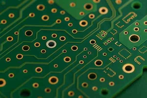
A Printed Circuit Board (PCB) has several types of holes. These include Plated Through-Holes (PTH) for component leads and vias, Non-Plated Through-Holes (NPTH) for mounting or tooling, and specialized holes like blind/buried vias, microvias, and castellated holes, each serving distinct electrical or mechanical functions.
You might think a hole is just a hole, but in PCB design, that's far from the truth. The type, size, and placement of each hole are critical decisions I make daily. These choices impact everything from electrical performance to the board's ability to be manufactured and assembled reliably. Let's explore these different holes. You need to understand them to make your next project a success.
What Are The Different Types Of Holes In PCB?
Confused by PCB hole jargon? It's easy to get lost. Understanding the main types helps you design better and communicate clearly with manufacturers.
PCB holes include Plated Through-Holes (PTH) for component leads and vias, Non-Plated Through-Holes (NPTH) for mechanical purposes, vias (through, blind, buried, microvias) for inter-layer connections, mounting holes for chassis attachment, and castellated holes for module-to-board soldering.
When I design a board, I'm constantly thinking about which hole type fits where. It's not just about drilling a hole; it's about its purpose.
Key PCB Hole Categories
Here's a breakdown of the common ones:
| Category | Sub-Type / Example | Description / Primary Purpose |
|---|---|---|
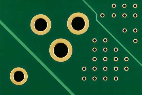
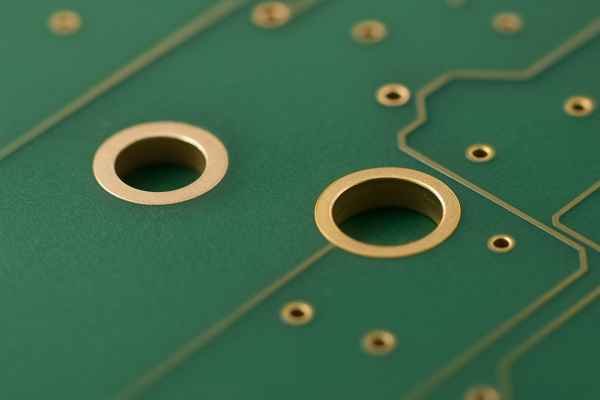
| Plated Through-Holes (PTH)1 | Component Holes | For leads of through-hole components, provides electrical connection. |
| Vias (Standard Through) | Electrically connect traces between different layers. | |
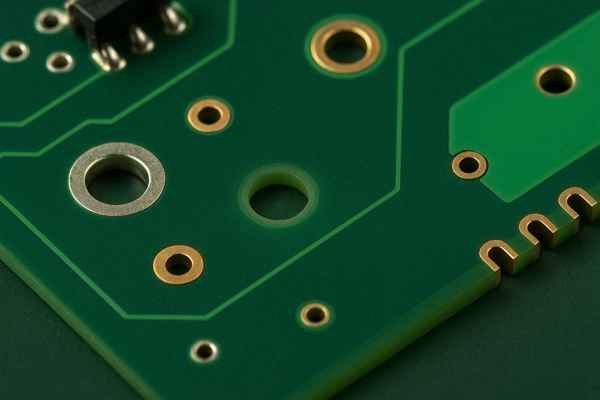
| Non-Plated Through-Holes (NPTH) | Mounting Holes | To screw the PCB to an enclosure or chassis; usually for isolation. |
| Tooling Holes | For alignment during manufacturing, assembly, or testing. | |
| Mechanical Holes | For standoffs, light pipes, or other non-electrical physical parts. | |
| Specialized Vias | Blind Vias2 | Connect an outer layer to an inner layer; don't go all the way through. |
| Buried Vias | Connect two or more inner layers; don't reach an outer layer. | |
| Microvias3 | Very small vias (≤ 0.15mm per IPC-2226), laser-drilled, for HDI PCBs. | |
| Other Specialized Holes | Castellated Holes | Plated half-holes on PCB edge for soldering a module board to another. |
Understanding these helps me select the right one for performance, cost, and manufacturability. For example, using blind/buried vias can increase density but also cost, a trade-off I always weigh.
What Is The Standard Hole PCB?
"Standard hole" sounds simple, right? But what does it really mean? It usually refers to holes for common leaded components, not a single universal size.
A "standard hole" on a PCB typically refers to a Plated Through-Hole (PTH) with a diameter suitable for common through-hole components, often ranging from 0.8mm (31.5 mils) to 1.0mm (39.4 mils) after plating, accommodating many resistor and capacitor leads.

When engineers talk about "standard holes," they're usually thinking about the Plated Through-Holes (PTHs) for traditional components with leads. There isn't one single "standard" size defined by a global body that fits everything. Instead, it's a range of common sizes.
Common PTH Sizes for Components
| Finished Hole Size (mm) | Approximate Size (mils) |
|---|---|
| 0.8 | 31.5 |
| 0.9 | 35.4 |
| 1.0 | 39.4 |
The drill size will be larger to account for the plating thickness. For instance, to achieve a 0.8mm finished hole, the drill might be 0.9mm if standard plating is 0.025mm (1 mil) per side.
IPC-2221B4 (Section 9.1.3) provides guidance on hole size relative to lead diameter:
| IPC-2221B Level | Minimum Hole Size Allowance (add to max lead diameter) |
|---|---|
| Level A | 0.25mm (most robust producibility) |
| Level B | 0.20mm (moderate producibility) |
| Level C | 0.15mm (least robust producibility, highest density) |
So, a 0.6mm lead would need at least a 0.8mm hole (0.6mm + 0.20mm) for a Level B fit. These are the "standards" I work with.
What Is The Most Common PCB Hole Size?
Wondering about the most frequent hole size on PCBs? It depends if you mean for components or vias. Both have their own typical dimensions.
For through-hole components, common finished hole sizes range from 0.8mm (31.5 mils) to 1.0mm (39.4 mils). For standard vias, common drill sizes are often 0.2mm (8 mils), 0.25mm (10 mils), or 0.3mm (12 mils).
Pinpointing the "most common" PCB hole size requires a bit of context.
For Through-Hole Components:
Sizes like 0.8mm, 0.9mm, and 1.0mm (finished hole diameter5) are very common.
| Finished Hole Diameter (mm) | Approx. Size (mils) | Example Use |
|---|---|---|
| 0.8 | 31.5 | Small diodes, resistor/capacitor leads |
| 0.9 | 35.4 | Standard resistor/capacitor leads |
| 1.0 | 39.4 | Larger diodes, some DIP IC pins, headers |
My experience with Tuxedo keypads at Honeywell involved many such components, and these sizes were staples.
For Vias:
Vias are generally smaller. Some of the most common drill sizes for standard through-hole vias I encounter are:
| Via Drill Size (mm) | Approx. Size (mils) | Approx. Finished Hole (mm) (with ~25µm plating per side) |
|---|---|---|
| 0.2 | 7.9 | 0.15 |
| 0.25 | 9.8 | 0.20 |
| 0.3 | 11.8 | 0.25 |
| 0.4 | 15.7 | 0.35 |
The finished hole size will be smaller due to plating. IPC-41016 specifies copper foil thicknesses, which indirectly affects plating. In high-density designs, I'd push for smaller vias, but these are very common general-purpose sizes.
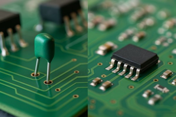
What Is The Through-Hole Called On A PCB?
Ever wondered about the correct term for a hole going through a PCB? It's simple, but knowing if it's plated or not makes a difference.
A hole that passes completely through a PCB is generally called a "through-hole." If it's plated for electrical conductivity, it's a "Plated Through-Hole" (PTH). If unplated, it's a "Non-Plated Through-Hole" (NPTH).
The term "through-hole" is quite descriptive: it's a hole that goes from one side of the PCB to the other. But in my engineering work, the key distinction is whether it's plated or not.
| Feature | Plated Through-Hole (PTH) | Non-Plated Through-Hole (NPTH) |
|---|---|---|
| Definition | A hole with conductive plating (usually copper) in its barrel. | A hole drilled without any subsequent conductive plating. |
| Primary Uses | 1. Mounting leaded components. 2. Vias (inter-layer connection). | 1. Mounting holes (for screws). 2. Tooling/alignment holes. 3. Mechanical support. |
| Creation | Drilled, then undergoes chemical plating processes. | Simply drilled. |
So, while "through-hole" is a general term, specifying PTH or NPTH gives a much clearer picture of its function, which is crucial when I'm reviewing designs or talking to fabricators.
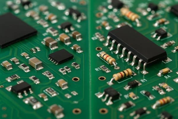
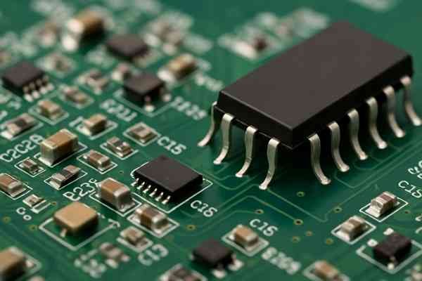
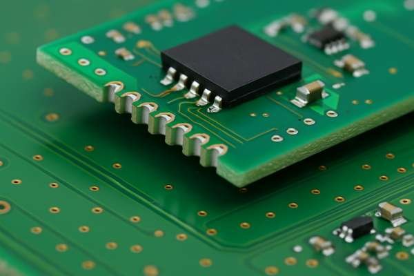
What Is The Difference Between SMT And Through-Hole PCB?
SMT and Through-Hole are two fundamental ways to build PCBs. One mounts on top, the other goes through. This choice impacts density, cost, and strength.
SMT (Surface Mount Technology) PCBs have components soldered directly onto the board's surface. Through-Hole Technology (THT) PCBs use components with leads inserted into plated holes and soldered from the opposite side. SMT allows for higher component density.
When I start a new hardware design, one of the first architectural decisions is the mix of Surface Mount Technology (SMT) and Through-Hole Technology (THT).
| Aspect | Through-Hole Technology (THT) | Surface Mount Technology (SMT) |
|---|---|---|
| Component Type | Components with wire leads. | Surface Mount Devices (SMDs) with small solderable terminations. |
| Mounting Method | Leads inserted through Plated Through-Holes (PTHs). | SMDs placed directly onto pads on PCB surface. |
| Soldering | Leads soldered to pads on the opposite side (e.g., wave soldering). | SMDs soldered to pads on the same side (e.g., reflow soldering). |
| Component Density | Lower. | Much higher, allows for smaller PCBs. |
| Mechanical Bond | Stronger, good for connectors and parts under stress. | Generally less robust for very large/heavy parts, but fine for most. |
| Assembly | Easier for manual work, more steps for automation. | Highly suited for automated assembly, can be harder for manual rework of small SMDs. |
| High Frequency | Longer leads can introduce parasitics. | Shorter connections, generally better performance. |
Many modern PCBs I design use a mix, with SMT for most components and THT for bulky connectors or power devices. My work on photonic computing chips heavily relied on SMT for density and speed.
What Is The Difference Between THT And SMT?
THT and SMT are core PCB assembly methods. One uses leads through holes, the other places parts on the surface. This affects everything from board size to performance.
THT (Through-Hole Technology) involves inserting component leads into drilled holes and soldering. SMT (Surface Mount Technology) places components directly onto surface pads. SMT enables smaller, denser designs, while THT often offers stronger mechanical connections.
Let's break down THT (Through-Hole Technology) and SMT (Surface Mount Technology) a bit more. I use both, and the choice often depends on the specific application needs.
Core Distinctions:
| Feature | Through-Hole Technology (THT) | Surface Mount Technology (SMT) |
|---|---|---|
| Component Mounting | Leads inserted through holes, soldered on other side | Components placed on surface pads, soldered on same side |
| Hole Requirement | Requires drilled Plated Through-Holes for leads | No through-holes needed for component leads |
| Component Size | Generally larger | Generally smaller (e.g., 0402, 0201 packages) |
| Density | Lower component density | Higher component density, can use both sides easily |
| Mechanical Strength | Typically stronger bond for components | Can be less robust for large/heavy components |
| Automation | Can be automated (wave soldering) but more steps | Highly suitable for full automation (pick-and-place) |
| High Frequency | Longer leads can introduce inductance/capacitance | Shorter paths, generally better HF performance |
| Prototyping/Rework | Easier for manual soldering and rework | Can be challenging for very small SMDs without tools |
For example, in the Tuxedo Keypad project, we used THT for connectors that faced frequent plugging/unplugging because the mechanical strength was crucial. For the dense processing sections, SMT was the only way to fit everything.
What Are The Advantages Of SMD Over Through-Hole?
SMDs seem to be everywhere now. Why? They offer big benefits in size, cost for mass production, and speed. Let's see why they often win out.
SMD (Surface Mount Device) components enable higher component density, reduced PCB size and cost, suitability for high-volume automated assembly, and generally better high-frequency performance due to smaller footprints and shorter electrical paths compared to through-hole components.
Surface Mount Devices (SMDs), used in SMT assembly, have become dominant in electronics. When I'm aiming for compact and high-performance designs, SMDs are usually my first choice.
Key SMD Advantages:
| Advantage | Description / Impact |
|---|---|
| Increased Component Density | SMDs are much smaller (e.g., 0402 resistor: 1mm x 0.5mm). More functionality in less space. |
| Reduced PCB Size & Weight | Higher density leads to smaller, lighter boards. Crucial for portable/space-constrained devices like medical pumps. |
| Lower Automated Assembly Cost | SMT is optimized for pick-and-place machines and reflow soldering, reducing high-volume assembly costs. |
| Improved High-Frequency Perf. | Very short/no leads minimize parasitic inductance/capacitance. Vital for high-speed digital and RF. |
| Better EMC Performance | Shorter signal paths and smaller loop areas can reduce EMI emissions and improve susceptibility. |
| Both Sides Mounting | SMDs can easily be mounted on both PCB sides, further boosting density. |
While THT still has its place for mechanical strength or specific components, the advantages of SMDs in terms of miniaturization, cost-effectiveness in volume, and electrical performance are often overwhelming.
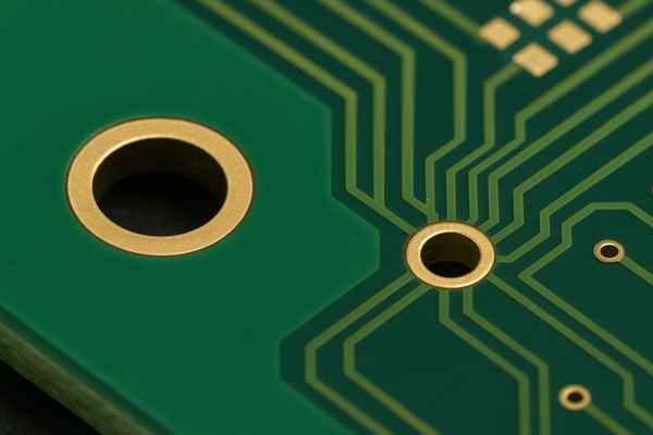
What Is The Difference Between A PCB Hole And Via?
Hole or via? They sound similar, but in PCB talk, a via has a very specific job. Not all holes are vias, but all vias are holes.
A "PCB hole" is any drilled opening. A "via" is a specific type of Plated Through-Hole (PTH) whose sole purpose is to create an electrical connection between different layers of the PCB. Component holes are also PTHs, but for mounting parts.
It's easy to get "hole" and "via" mixed up, but the distinction is important.
| Term | Definition | Key Characteristics |
|---|---|---|
| PCB Hole | Any perforation drilled or formed in the PCB. (Broad term) | Can be Plated (PTH) or Non-Plated (NPTH). Used for components, mounting, alignment, or inter-layer connection. |
| Via | A specialized Plated Through-Hole (PTH). (Vertical Interconnect Access) | Sole purpose is electrical connection between layers. Always plated. Typically no component lead inserted. Can be through, blind, buried, or micro. |
So, all vias are holes (specifically, PTHs), but not all holes are vias. For example, the PTHs I use for resistor leads are holes, but not vias. The small PTHs I place to route a signal from the top layer to an inner layer are vias.
What Are Castellated Holes On A PCB?
Ever seen those half-holes on the edge of a module? Those are castellated holes. They're clever for connecting boards together like big SMD components.
Castellated holes are Plated Through-Holes (PTHs) located on the edges of a PCB that are cut in half, creating semi-circular, plated indentations. They allow one PCB module to be easily soldered onto another main board using SMT techniques.
Castellated holes, sometimes called "castellations" or "half-holes," are a neat feature I've used for designing modular systems.
How They Work:
- Creation: Regular Plated Through-Holes are drilled along the edge(s) of the PCB module.
- Cutting: During PCB de-panelization, the board edge is routed through the center of these PTHs.
- Result: This leaves semi-circular, plated notches along the module edge.
Purpose and Advantages:
- Module Integration: Allows the module PCB to be treated like a large SMD for SMT assembly.
- Reliable Connection: Plated surface ensures good solderable contact.
- Space Saving: Can be more compact than connectors.
- Visual Inspection: Solder joints are typically easy to inspect.
When I design with castellated holes (e.g., with a 1.27mm pitch using original 0.8mm PTHs), I specify pad design on the main board carefully for good solder fillets.
What Does The Square Hole In A PCB Mean?
Seen a square hole or pad on a PCB and wondered why? It's usually a visual cue. Most often, it marks pin 1 of a component for easy orientation.
A square hole itself is uncommon, but a square pad associated with a round through-hole is frequently used to indicate Pin 1 of a component, like an IC or connector. This helps with correct orientation during assembly and inspection.
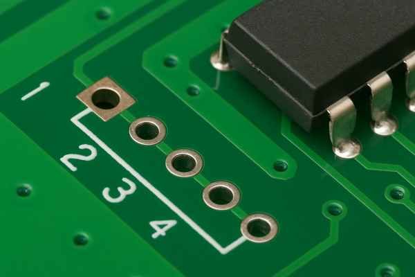
It's rare to see a truly square drilled hole. You're more likely to see a square-shaped solder pad with a round Plated Through-Hole (PTH).
| Feature | Primary Meaning / Use | Other (Less Common) Possibilities |
|---|---|---|
| Square Pad (with round hole) | Pin 1 Indicator for components (ICs, connectors). | Maximize copper area for high current (hole still round). |
| Provides clear visual cue for correct orientation. | ||
| Square Drilled Hole (rare) | Mechanical keying for specific connectors. |
The square pad for Pin 1 is a strong industry convention (discussed in IPC-2221 for orientation markings) that I consistently use to prevent assembly errors.
Conclusion
Understanding PCB holes – PTH, NPTH, vias, mounting, mechanical – is key. Proper selection impacts your design's success, from electrical performance to mechanical stability and cost.
-
Explore this link to understand the significance of PTH in PCB design and how they enhance electrical connections. ↩
-
Learn about Blind Vias and how they can optimize PCB layout and performance, especially in high-density designs. ↩
-
Discover the benefits of Microvias in HDI PCBs and how they contribute to miniaturization and performance. ↩
-
Exploring IPC-2221B will provide you with essential guidelines for PCB design, ensuring optimal hole sizes and manufacturability. ↩
-
Understanding finished hole diameter is crucial for ensuring proper component fit and functionality in PCB design. ↩
-
IPC-4101 provides essential guidelines for copper foil thickness, impacting the quality and reliability of PCB designs. ↩


