 Skip to content
Struggling with noisy PCB designs or unexpected failures? Your PCB layer stackup might be the hidden culprit. Proper planning here is key to success.
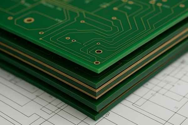
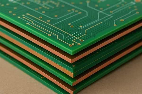
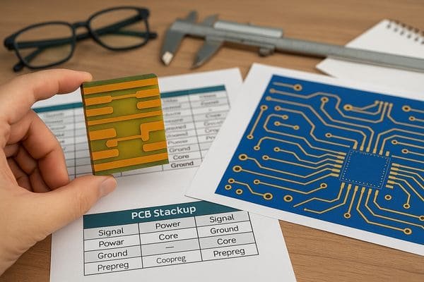
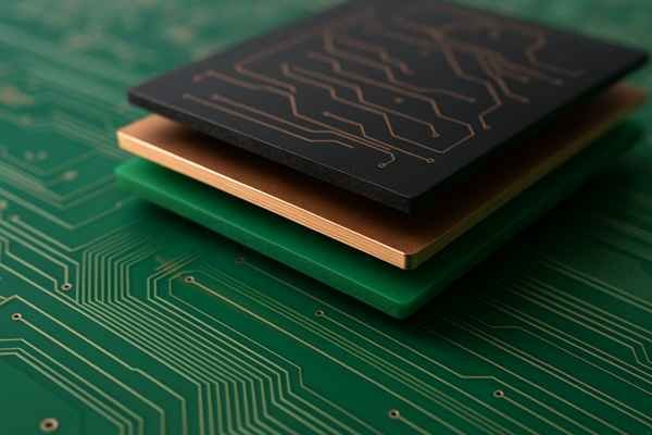
Planning a multilayer PCB stackup involves carefully defining the order of copper and insulating layers, their materials, and thicknesses. This ensures signal integrity, manages controlled impedance, provides clear return paths, minimizes electromagnetic interference (EMI), and optimizes manufacturability for reliable electronic performance.
I've seen many projects stumble because the stackup was an afterthought. It’s a foundational part of your design. If you get it right, many potential problems simply vanish. Let's look deeper into why this is so crucial and how you can master it.
Why Is a Proper PCB Stackup Important?
Are signal glitches, crosstalk, or EMI issues derailing your projects? An improperly designed stackup is often the silent saboteur. A well-thought-out stackup prevents these headaches.
A proper PCB stackup is vital for achieving target controlled impedances, ensuring good signal integrity by providing clean return paths, minimizing crosstalk between traces, reducing electromagnetic emissions, and improving the power delivery network's performance. It directly impacts reliability and manufacturability.
The Critical Impact of Stackup on Performance
A proper PCB stackup is far more than just fitting all your connections onto a board. It’s fundamental to the electrical performance of your entire system. I've seen firsthand how a well-engineered stackup can be the difference between a product that sails through testing and one that’s plagued by mysterious issues.
The stackup dictates several critical electrical characteristics. My insight here is that the return path continuity1, often overlooked, is paramount. A signal doesn't just travel on a trace; it travels in a loop, and the return path through an adjacent plane is critical. Discontinuities here are major noise sources. Strategically placed power and ground planes with tight coupling can also significantly reduce the need for discrete decoupling capacitors, especially for high-frequency noise. I’ve found that aiming for an interplane capacitance2 by keeping power and ground planes physically close (e.g., 3-5 mils or 0.076mm - 0.127mm apart) makes a huge difference.
Here's how a well-designed stackup contributes to key performance aspects:
| Performance Aspect | Benefit of Proper Stackup |
|---|---|
| Signal Integrity (SI) | Reduced reflections, minimized crosstalk, clear signal paths. |
| Power Integrity (PI) | Stable power delivery, lower noise, effective decoupling. |
| EMC/EMI | Lower electromagnetic emissions, improved immunity to noise. |
| Impedance Control | Consistent trace impedance for high-speed signals. |
| Manufacturability | Higher production yield, reduced warping, lower overall cost. |
| Reliability | Reduced stress on components, longer product lifespan. |
A poorly designed stackup can lead to increased prototype iterations, difficult debugging, and even field failures. It’s an area where initial careful planning pays huge dividends later.
How to Decide the Number of Layers in PCB?
Wondering if two, four, or more layers are needed for your next PCB? This decision impacts cost and performance. Choosing correctly avoids over-engineering or under-designing.
The number of PCB layers depends on circuit complexity, signal routing density, the quantity of high-speed signals needing controlled impedance, EMC requirements, and power distribution needs. Cost is also a major factor; more layers mean higher fabrication expenses.
Balancing Complexity, Performance, and Cost
Deciding on the number of layers for your PCB is a balancing act. You need enough layers for all your signals, power, and ground, but each additional layer pair adds to the cost. Here’s my approach:
Key factors include:
- Signal Density and Complexity: How many nets do you have? Are they high-speed? Devices like FPGAs or modern processors with hundreds of BGA pins often necessitate more layers simply to escape all the signals.
- Controlled Impedance Requirements: If you have many signals that require precise impedance control (e.g., USB, Ethernet, DDR memory), you'll likely need dedicated reference planes (ground or power) adjacent to these signal layers.
- EMC Performance3: For good EMC, at least four layers are generally recommended for anything beyond very simple, low-speed designs.
- Power Distribution4: Multiple power rails might need their own dedicated layers or split planes for clean distribution.
- Component Density and Type: High-density SMT components or BGAs with fine pitches might require more layers for fanout.
Here's a general comparison:
| Layer Count | Typical Application | Relative Cost | EMC Performance | Routing Density |
|---|---|---|---|---|
| 2 Layers | Simple, low-frequency, hobbyist projects | Lowest | Poor | Low |
| 4 Layers | Moderately complex, good EMC baseline | Low-Medium | Good | Medium |
| 6 Layers | High-speed signals, dense routing | Medium | Very Good | High |
| 8+ Layers | Very complex, multiple high-speed buses | High | Excellent | Very High |
A 4-layer board typically adds 30-50% to the bare board cost compared to a 2-layer board of the same size and quantity. For example, if a 100x100mm 2-layer prototype costs $5, a 4-layer might cost $7-$8. Each additional pair of layers (e.g., 4 to 6, 6 to 8) can add another 20-40% to the cost. A 6-layer version of that $5 board might be $10-$12. These are very rough estimates. I always start by evaluating BGA fanout and high-speed interface requirements. If I have a DDR3/4 interface, I'm likely looking at a minimum of 6 or 8 layers.
What Are the Rules for PCB Layer Stackup?
Are there "golden rules" for arranging PCB layers? Yes, following established guidelines prevents common signal integrity and EMI problems. Get these rules right for a robust design.
Key rules include: placing signal layers adjacent to solid reference planes (ground or power), ensuring tight coupling between power and ground planes, maintaining return path continuity, avoiding routing high-speed signals across plane splits, and aiming for a symmetrical stackup.
Fundamental Principles for Robust Stackup Design
Over my years in hardware design, I've learned that following a few fundamental rules for PCB layer stackup can save countless hours of debugging. These are based on the physics of electromagnetism. My key insight remains: return path continuity is critical5.
Here's a summary of core stackup design principles:
| Rule | Benefit | Why It's Important |
|---|---|---|
| Signal Layers Adjacent to Planes | Controlled impedance, defined return path | Minimizes loop area, reduces noise and crosstalk. |
| Tight Power/Ground Coupling | Improved high-frequency decoupling6, reduced power supply noise | Creates beneficial interplane capacitance. |
| Solid (Unbroken) Reference Planes | Consistent return path, stable impedance | Prevents return currents from taking long, noisy paths. |
| Avoid Routing Across Plane Splits | Maintains return path integrity, prevents large current loops | Large loops radiate EMI and degrade signal quality. |
| Symmetrical Stackup Construction | Prevents board warp/twist, ensures manufacturing stability | Balances mechanical stresses during fabrication. |
| High-Speed Signals on Inner Layers | Better shielding, more consistent impedance | Sandwiched between planes for protection. |
| Isolate Noisy and Sensitive Signals | Prevents interference | Physical separation and shielding by planes. |
Adhering to these rules, like those outlined in standards such as IPC-2221 (Generic Standard on Printed Board Design), forms the bedrock of a good stackup design.
How to Design a PCB Stackup?
Ready to define your own PCB stackup but unsure where to start? There's a systematic process to follow. Designing it methodically ensures optimal performance and manufacturability.
Design a PCB stackup by first determining layer count, then assigning functions to each layer (signal, power, ground). Next, select materials (core, prepreg, copper weight), define dielectric thicknesses, calculate impedance for critical traces, and finally, consult with your PCB manufacturer.
A Step-by-Step Approach to Stackup Design
Designing a PCB stackup is an engineering task that should happen early in the design cycle. Here’s a step-by-step approach I typically follow:
| Step | Key Considerations & Actions |
|---|---|
| 1. Determine Layer Count | Based on signal density, BGA fanout, high-speed interfaces (e.g., DDR, PCIe), power requirements, and EMC needs. |
| 2. Assign Layer Functions | Define each layer: Signal, Ground, Power. Ensure signal layers are adjacent to reference planes. E.g., 6-layer: SIG-GND-SIG-PWR-GND-SIG. |
| 3. Select Materials | Choose laminate (FR-4, Rogers, Megtron based on frequency/loss), copper weight (0.5oz, 1oz, 2oz). Consult material datasheets (e.g., Isola, Rogers Corp). |
| 4. Define Dielectric Thicknesses | Specify core and prepreg thicknesses. Crucial for impedance and interplane capacitance. E.g., target 3-5 mils between PWR/GND planes. |
| 5. Calculate Controlled Impedances | Use EDA tools or calculators (IPC-2141 based) for required trace widths (e.g., 50Ω single-ended, 90/100Ω differential) based on stackup parameters. |
| 6. Consult Your Manufacturer | Vital step! Share proposed stackup. Get feedback on material availability, manufacturability, tolerances. They may offer cost-effective standard stackups. |
I always create a detailed stackup drawing or table specifying layer names, material types, thicknesses, copper weights, and target impedances. This leaves no room for ambiguity.
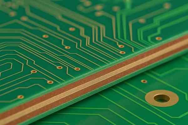
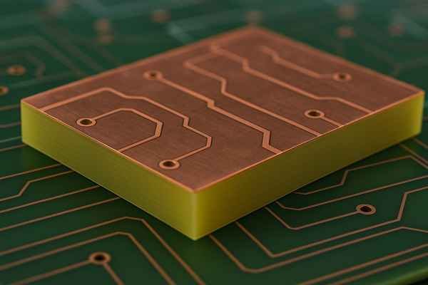
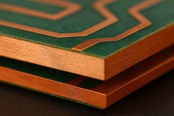
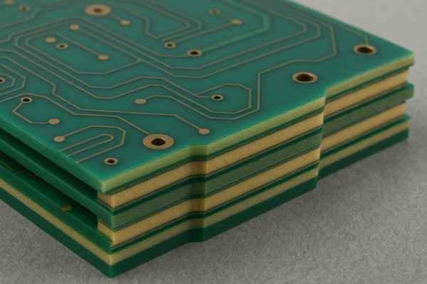
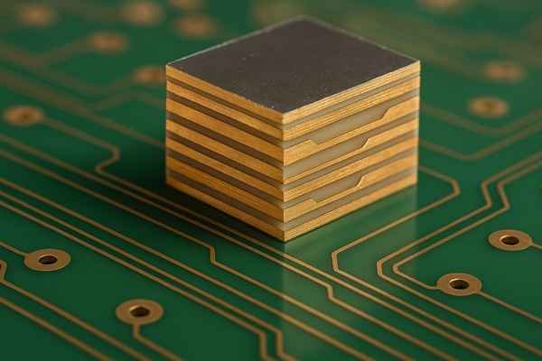
What Is a "Core" in a PCB Stackup?
Heard the term "core" when discussing PCB stackups? It's a fundamental building block. Understanding cores helps you grasp how multilayer boards are constructed.
A "core" in a PCB stackup is a rigid piece of dielectric material (like FR-4) with copper foil laminated to one or both sides. Its dielectric thickness is fixed and well-controlled, forming a stable base for PCB layers.
Understanding PCB Core Materials
When we talk about the construction of a multilayer PCB, the term "core" refers to a primary building block. Think of it as a pre-made, rigid piece of circuit board material.
Its key characteristics include:
- Composition: A core consists of a layer of cured dielectric material, typically woven glass reinforced epoxy resin like FR-4. Copper foil is bonded to one or both sides.
- Fixed Thickness: The dielectric thickness of a core is manufactured to a specific, well-controlled value. Common core dielectric thicknesses might range from 0.004 inches (4 mils or ~0.1 mm) to 0.062 inches (62 mils or ~1.57 mm). For example, a manufacturer might stock FR-4 cores with dielectric thicknesses of 0.2mm, 0.4mm, 0.8mm, etc., with specific copper weights already clad (e.g., 0.5 oz, 1 oz).
- Role in Stackup: In a multilayer PCB, one or more cores are used. For instance, a 4-layer PCB often uses one central core with copper on both sides (acting as Layer 2 and Layer 3).
- Stability: Cores provide dimensional stability.
When I design a stackup, I often start by selecting the core(s) because their thicknesses are more predictable than prepreg layers. This is beneficial for critical controlled impedance traces adjacent to a core.
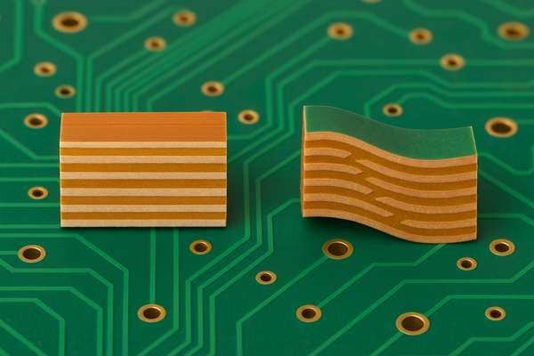
What Is "Prepreg" in a PCB Stackup?
What exactly is "prepreg" in the world of PCB manufacturing? It's the glue that holds multilayer boards together. Knowing its role is key to understanding stackup design.
"Prepreg" is a B-stage composite material made of woven glass cloth impregnated with a partially cured resin. In PCB stackups, it acts as an adhesive to bond layers together and provides insulation between copper layers during lamination.
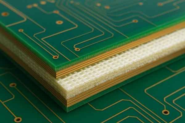
The Role of Prepreg in Multilayer Construction
"Prepreg" is short for "pre-impregnated" composite fibers. It plays a crucial role in bonding the different layers of a multilayer PCB together and also acts as a dielectric.
Its properties and role are:
- Composition: Fiberglass cloth saturated with a partially cured "B-stage" resin (usually epoxy).
- Adhesive: During lamination (heat and pressure), the resin flows, fills gaps, and cures ("C-stage"), bonding layers.
-
Dielectric Layer: Forms an insulating layer. Thickness depends on the type and number of prepreg sheets used. Common prepreg glass styles and their approximate pressed thicknesses:
Prepreg Style Typical Pressed Thickness (per sheet) 106 ~1.5-2.0 mils (0.038-0.051 mm) 1080 ~2.5-3.0 mils (0.063-0.076 mm) 2113 ~3.5-4.0 mils (0.089-0.102 mm) 2116 ~4.5-5.0 mils (0.114-0.127 mm) 7628 ~6.5-7.5 mils (0.165-0.190 mm) (Actual pressed thickness can vary based on copper patterns and fab process).
When designing a stackup, I specify the type or target thickness for prepreg layers to achieve desired dielectric spacing, crucial for controlled impedance. For example, two sheets of 1080 prepreg might be used to achieve around 5-6 mils.
What Materials Are Used in PCB Stackup?
Beyond "green," what are PCBs actually made of? The choice of materials in a stackup critically affects performance and cost. Knowing your options is important for any design.
Common PCB stackup materials include FR-4 (a glass-reinforced epoxy laminate), high-frequency laminates (like Rogers or Panasonic Megtron series), polyimide (for flexible PCBs), copper foil for conductive layers, and prepregs (resin-impregnated glass cloth) for bonding and insulation.
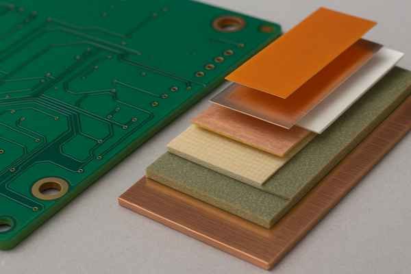
A Look at Common PCB Materials
The choice of materials for a PCB stackup is crucial. I’ve worked with a range of materials depending on project needs.
| Material Category | Example(s) | Dielectric Constant (\(D_{k}\) @ 1GHz) | Loss Tangent (\(D_{f}\) @ 1GHz) | Relative Cost | Typical Application |
|---|---|---|---|---|---|
| Standard Epoxy | FR-4 (Tg 130-180°C) | ~4.0 - 4.8 | ~0.015 - 0.025 | Low | General purpose, low-mid frequency digital/analog |
| High-Speed/RF | Rogers RO4003C, RO4350B; Panasonic Megtron 6 | ~3.3 - 3.7 (RO4350B: 3.48) | ~0.002 - 0.004 | High | High-frequency RF, microwave, very high-speed digital |
| Flexible Substrate | Polyimide (Kapton) | ~3.2 - 3.5 | ~0.002 - 0.007 | Medium-High | Flexible circuits, rigid-flex PCBs |
| Conductive | Copper Foil (ED or RA) | N/A | N/A | N/A | Traces, planes, pads |
| Bonding | Prepreg (FR-4 based, or compatible with laminate) | Similar to core material | Similar to core material | Low-Medium | Layer bonding, insulation |
\(D_{k}\) and \(D_{f}\) values are approximate and vary with frequency, resin content, and specific product grade. Always refer to manufacturer datasheets (e.g., Isola, Rogers Corporation, Panasonic) for precise values.
Copper weights are typically 0.5 oz (17.5 µm), 1 oz (35 µm), or 2 oz (70 µm). When I worked on a photonic computing chip interface at 25 Gbps, FR-4 was inadequate; a material like Rogers RO4350B was necessary.
What Is the Clearance Between PCB Layers?
How much space is actually between the copper layers in your PCB? This "clearance," or dielectric thickness, is a critical design parameter. Understanding it helps control impedance and capacitance.
The clearance between PCB layers is the thickness of the dielectric (insulating) material separating them. This is determined by the chosen core and prepreg thicknesses, typically ranging from 2 mils (0.0508 mm) to over 60 mils (1.524 mm).
Understanding Dielectric Thickness
The "clearance" between PCB layers, more accurately termed dielectric thickness, is fundamental to the stackup.
It is determined by:
- Core Thickness: Pre-defined dielectric thickness of the core material, e.g., 0.004 inches (4 mils or ~0.1 mm) to 0.059 inches (59 mils or ~1.5 mm).
- Prepreg Thickness: Determined by the type and number of prepreg sheets used (see table in "What Is 'Prepreg'?" section). For example, a single ply of 1080 glass style prepreg typically yields a pressed thickness of 2.5-3.0 mils.
Why clearance matters:
- Controlled Impedance: Dielectric thickness (\(H\)) is a primary factor. Impedance often decreases as \(H\) decreases.
- Interplane Capacitance: Clearance between power and ground planes determines capacitance. Smaller clearance (e.g., 3-5 mils or 0.076mm - 0.127mm) means higher capacitance, aiding high-frequency decoupling. I aim for this.
- Voltage Breakdown: Standard PCB materials typically offer high dielectric breakdown voltage (e.g., 500-1500 V/mil, source: general material datasheets). This is rarely an issue for low-voltage designs but becomes relevant for high-voltage applications.
I always define target dielectric thicknesses. For instance, between a high-speed signal layer and its ground reference, I might target 4 mils +/- 0.5 mils.
How Can Layer Order Affect EMI/EMC Performance?
Can simply reordering your PCB layers impact its noise emissions? Absolutely. Strategic layer arrangement is a powerful tool for controlling EMI and ensuring EMC compliance.
Layer order significantly affects EMI/EMC by dictating signal return paths, shielding effectiveness, and loop areas. Placing signal layers adjacent to solid ground planes and keeping power/ground planes closely coupled minimizes emissions and improves immunity.
Strategic Layer Ordering for EMI Control
The order of layers profoundly impacts EMI generation7 and EMC. I’ve seen designs pass or fail EMC testing8 based almost entirely on stackup choices, like during the Tuxedo Keypad project with its strict global certifications (FCC, CE, VdS).
| Stackup Strategy | EMI/EMC Benefit |
|---|---|
| Solid Ground Planes Adjacent to Signals | Provides low-inductance return paths, minimizes signal loop areas, reduces common-mode radiation. |
| Outer Layer Ground Planes | Act as shields, protecting internal circuitry from external noise and reducing emissions from the board. |
| Tight Power/Ground Plane Coupling | Creates distributed capacitance, effective for high-frequency decoupling, reduces PDN noise and emissions. |
| High-Speed Signals on Inner Layers | Shields fast signals between reference planes, reducing radiation and susceptibility. |
| Avoid Large Gaps in Reference Planes | Ensures continuous return paths, preventing signals from detouring and creating larger, radiating current loops. |
Example Stackups:
- 4-Layer (Good EMC):
Signal 1 (Top) - GND - PWR - Signal 2 (Bottom). Provides good referencing. - 4-Layer (Poor EMC if planes far apart/gapped):
Signal 1 (Top) - PWR - GND - Signal 2 (Bottom). - 6-Layer (Very Good EMC):
Signal 1 - GND - Signal 2 - PWR - GND - Signal 3. Excellent shielding.
Routing critical clock signals or fast data lines on inner layers, sandwiched between ground planes, was a common strategy for us. This again highlights my core insight: explicitly engineering return path continuity is crucial for EMC.
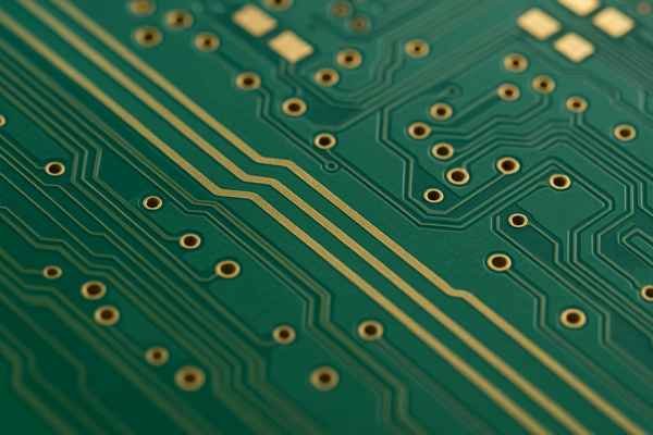
What Is Controlled Impedance in PCBs?
Heard "controlled impedance" but not sure what it means for your PCBs? It's essential for high-speed signals. Understanding it prevents signal degradation and ensures data integrity.
Controlled impedance in PCBs is the design and manufacturing of traces to achieve a specific characteristic impedance, typically 50 ohms single-ended or 90/100 ohms differential. This matches transmission line impedance, minimizing signal reflections and ensuring signal integrity for high-speed circuits.
The Basics of Transmission Lines on PCBs
When signals switch fast enough, PCB traces act like transmission lines, each with a characteristic impedance (\(Z_{0}\)). If trace impedance doesn't match driver/receiver impedance, reflections occur, causing signal distortion.
Common impedance values and sources:
- 50 Ohms Single-Ended: Standard for many RF, general logic.
- 90 Ohms Differential: USB 2.0 High-Speed data lines (D+/D-). (Source: USB-IF specifications).
- 100 Ohms Differential: Ethernet, LVDS, HDMI, SATA, USB 3.x, PCIe. (Source: Respective standards bodies like IEEE for Ethernet, JEDEC for LVDS, PCI-SIG for PCIe).
A rule of thumb: controlled impedance is needed if trace length > (1/10 to 1/6) of the signal's electrical wavelength corresponding to its fastest rise/fall time. For a 1 ns rise time (\(f_{k} \approx 0.5 / t_{r} = 500 \text{ MHz}\)), wavelength in FR-4 (\(D_{k} \approx 4\)) is ~30 cm. Traces > 3-5 cm likely need it. For the Tuxedo Keypad's Wi-Fi antenna feedline, a precise 50-ohm impedance was critical.
For more details, you can refer to my article: Mastering PCB Impedance Control: A Practical Engineer’s Guide
How Does the PCB Stackup Affect Controlled Impedance?
If controlled impedance is key, how does your PCB layer arrangement influence it? The stackup is foundational. It defines the parameters that determine trace impedance.
The PCB stackup directly affects controlled impedance by defining critical geometric and material properties: dielectric material type (its dielectric constant, \(D_{k}\)), the thickness of the dielectric between a trace and its reference plane(s), and trace copper thickness.
Stackup's Direct Influence on Impedance Values
The PCB stackup is the blueprint dictating the electrical environment for traces. You can't get controlled impedance right if your stackup isn't well-defined.
| Stackup Parameter | Symbol | Effect on Impedance (\(Z_{0}\)) | Source in Stackup |
|---|---|---|---|
| Dielectric Constant | \(D_{k}\) | \(Z_{0} \propto 1/\sqrt{D_{k}}\) (Higher \(D_{k}\) means lower \(Z_{0}\)) | Laminate material choice |
| Dielectric Height | \(H\) | \(Z_{0} \propto \ln(H)\) (Higher \(H\) means higher \(Z_{0}\)) | Core/prepreg thickness |
| Trace Width | \(W\) | \(Z_{0} \propto 1/W\) (Wider \(W\) means lower \(Z_{0}\)) | Designer's choice, calculated |
| Trace Copper Thickness | \(T\) | Slight: thicker \(T\) slightly lowers \(Z_{0}\) | Copper weight selection |
| Reference Plane Proximity | N/A | Closer planes (stripline) generally lower \(Z_{0}\) vs microstrip | Layer arrangement |
An approximate formula for microstrip impedance (from IPC-2141, though EDA tools use more complex field solvers):
\(Z_{0} \approx \frac{87}{\sqrt{D_{k} + 1.41}} \ln\left(\frac{5.98 \times H}{0.8 \times W + T}\right)\) Ohms.
\(D_{k}\), \(H\), and \(T\) come directly from the stackup. The designer calculates \(W\) to hit the target \(Z_{0}\). For example, 50Ω on an outer layer with 1 oz copper (\(T\)=1.37 mils), FR-4 (\(D_{k} \approx 4.2\)), and dielectric height \(H\) of 5 mils might need \(W\) ~ 8-9 mils.
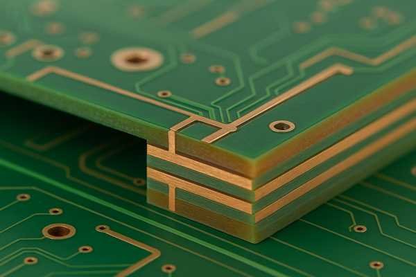
What Is a Symmetrical Stackup?
You might hear PCB fabs prefer "symmetrical" stackups. What does this mean? It's about balance in the PCB construction. Understanding this helps prevent manufacturing problems.
A symmetrical PCB stackup means the layer types, copper weights, and dielectric thicknesses are mirrored around the PCB's central plane. This balanced construction helps prevent warping and twisting during fabrication and thermal cycling, ensuring mechanical stability.

The Importance of Balance in Construction
A symmetrical stackup mirrors materials and thicknesses from the top half to the bottom half, relative to the PCB's center. Layer 1 properties (copper, prepreg) should match layer 'n'; layer 2 with 'n-1', etc.
Why symmetry is vital (as per IPC-2221A, Section 9.1.6 - Balanced Construction):
- Prevents Warp and Twist9: Different materials expand/contract at different rates. Symmetry balances these forces, keeping the board flat during lamination and thermal cycling. This is critical for SMT assembly.
- Manufacturing Stability: More predictable results and higher yields for fabricators.
I always push for symmetrical stackups. The risk of a warped board (a "potato chip") is too high otherwise.
What Is an Asymmetrical Stackup?
If symmetry is good, what is an asymmetrical stackup? It's a PCB construction lacking that mirror image. While sometimes used, it carries risks that designers must understand.
An asymmetrical PCB stackup is one where the layer types, copper weights, or dielectric thicknesses are not mirrored around the PCB's central plane. This unbalanced construction can lead to warping, twisting, and other manufacturing or reliability issues.
Risks of Unbalanced PCB Construction
An asymmetrical stackup lacks that mirrored balance. For instance, Layer 1 might be 1 oz copper while the bottom layer is 0.5 oz, or dielectric thicknesses might differ.
Why generally avoid asymmetrical stackups:
- Warp and Twist: Unbalanced stresses from material expansion/contraction cause boards to bow. This is a nightmare for assembly and can compromise solder joint reliability.
- Manufacturing Challenges: Less predictable for fabricators.
- Reliability Concerns: Internal stresses can be exacerbated by thermal cycling, leading to delamination or via failures.
I've seen boards come out of reflow badly warped due to asymmetry. It's a situation best avoided unless absolutely no other option exists and the fabricator agrees.
Should I Use Symmetrical or Asymmetrical Stackups?
Facing the choice between symmetrical and asymmetrical PCB stackups? The answer is usually clear-cut. One offers stability and reliability, the other poses significant risks.
You should almost always use symmetrical PCB stackups. Symmetrical designs prevent warping, ensure manufacturing stability, and improve overall reliability. Asymmetrical stackups should only be considered in rare, highly specialized cases with full manufacturer consultation and acceptance of risks.
The Clear Choice for Stability and Reliability
The recommendation is overwhelmingly for symmetrical stackups. My nearly 20 years in hardware development strongly reinforce this.
| Feature | Symmetrical Stackup | Asymmetrical Stackup |
|---|---|---|
| Mechanical Stability | High (prevents warp/twist) | Low (prone to warp/twist) |
| Manufacturability | Predictable, higher yield | Challenging, lower yield, riskier |
| Reliability | Generally higher | Potentially lower due to internal stress |
| Assembly | Easier, SMT friendly (flat boards) | Difficult if warped |
| Industry Standard | Strongly recommended (e.g. IPC-2221A) | Generally advised against |
Asymmetrical stackups are a last resort, only if extreme design constraints exist and the fabricator explicitly agrees, understanding the risks. The potential headaches usually outweigh any perceived benefit. Aim for symmetry always.
What Stackup Information Does a PCB Manufacturer Need?
Ready to send your design to the fab house? Providing clear stackup details is crucial. Missing information leads to delays and potential errors in your boards.
A PCB manufacturer needs a detailed layer stackup including: layer order, material types (e.g., FR-4, Rogers), dielectric thickness for each insulating layer, copper weight for each conductive layer, overall board thickness with tolerance, and any controlled impedance requirements (target impedance, layers, trace widths).
Ensuring Clear Communication with Your Fab House
Comprehensive stackup information is critical. Ambiguity leads to errors. I always provide a detailed stackup diagram or table.
Here's a checklist of essential information:
| Information Category | Details to Provide |
|---|---|
| Layer Order & Type | List layers top to bottom (e.g., L1 Top, L2 GND, L3 SIG, L4 PWR...). Specify type (Signal, Plane, Mixed). |
| Material Specifications | Laminate type (e.g., "FR-4, Tg 170°C", "Rogers RO4350B"), specific prepreg types if known/critical. |
| Dielectric Thicknesses | Desired thickness for each insulating layer (core dielectric, prepreg). Include tolerances if critical (e.g., "0.004 inches +/- 10%"). |
| Copper Weights | For each conductive layer (starting foil & final plated). E.g., "L1: 0.5 oz (17.5 µm) finished", "L2 (GND): 1 oz (35 µm) finished". |
| Overall Board Thickness | Final desired thickness with tolerance (e.g., "1.57 mm +/- 0.15 mm"). |
| Controlled Impedance | Layer(s), target impedance(s) (e.g., "50Ω +/-10%"), design trace width(s), reference layer(s). E.g., "L1: 5 mil traces, 50Ω ref L2". |
| Surface Finish | E.g., ENIG, HASL, OSP (though not strictly stackup, it's key fab data). |
| File Names for Each Layer | Ensure Gerber/ODB++ file names clearly correspond to the stackup description. |
Many EDA tools can generate this report. Clear communication prevents costly mistakes.
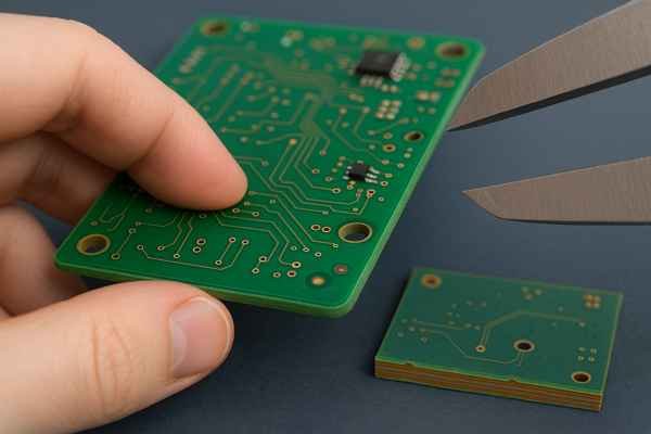
How Do You Determine How Many Layers a PCB Has?
Got a PCB in hand but unsure how many layers it contains? There are a few ways to find out. Knowing the layer count can be important for reverse engineering or understanding a design.
To determine a PCB's layer count, visually inspect the edges for distinct layers or vias connecting different levels. Silkscreen markings might indicate it. If available, consult design files or manufacturer specs. For unknown boards, cross-sectioning (destructive analysis) is definitive.
Methods for Identifying PCB Layer Count
Determining the layer count of an existing PCB can vary in difficulty.
| Method | Description | Reliability | Destructive? |
|---|---|---|---|
| Visual Edge Inspection | Examine edges for distinct laminate/copper lines. Magnification helps. | Low to Medium | No |
| Via Structure Analysis | Look for through-hole, blind, or buried vias. Blind vias indicate internal layers. | Medium | No |
| Silkscreen Markings | Check for layer count or part numbers indicating layers printed on the board. | Low (if present) | No |
| Design Documentation/Files | Gerber, ODB++, CAD files, fab specs explicitly state layer count. | Very High | No |
| Manufacturer Datasheet | For COTS boards, specs often list layer count. | High | No |
| Infer from Component Density | Very fine-pitch BGAs (e.g., <0.5mm) usually imply multiple layers (6+). | Medium | No |
| Cross-Sectioning | Cut, mount, polish, and microscopically examine a sample. | Definitive | Yes |
For a quick assessment, I start with edge inspection and via types. If I were reverse-engineering an undocumented module, cross-sectioning would be the ultimate, albeit destructive, method.
Conclusion
Proper PCB stackup planning is essential for signal integrity, EMC, and manufacturability. It’s a foundational step that ensures your electronic designs perform reliably and meet specifications.
-
Understanding return path continuity is crucial for ensuring signal integrity and reducing noise in PCB designs. Explore this link to enhance your knowledge. ↩
-
Interplane capacitance plays a vital role in reducing noise and improving performance. Discover more about its impact on PCB design. ↩
-
EMC performance is vital for reducing interference and ensuring compliance. Learn more about its impact on PCB design by exploring this resource. ↩
-
Effective power distribution is key to reliable PCB operation. Discover best practices to enhance your designs by checking this link. ↩
-
Understanding the importance of return path continuity can significantly enhance your PCB design, leading to fewer issues and better performance. ↩
-
Learning about high-frequency decoupling can provide insights into reducing power supply noise, crucial for high-performance electronics. ↩
-
Understanding EMI generation is key to improving your designs and ensuring compliance with regulations. Explore this resource for expert insights. ↩
-
Preparing for EMC testing is essential for product success. This resource will guide you through effective strategies and tips. ↩
-
Exploring this topic will reveal how symmetry is crucial for maintaining the integrity of PCBs during production. ↩


