 Skip to content
Struggling with manufacturing small circuit boards? The handling costs and manual processes can kill your project's budget and timeline. But worse, a poorly planned panel can introduce defects that haunt you in production. Proper panelization is the key to efficient, reliable, and cost-effective automated assembly.
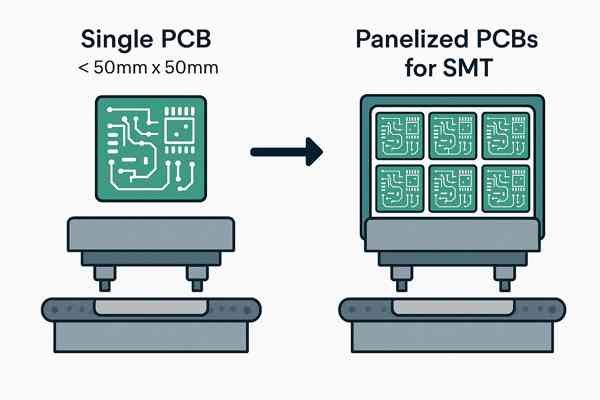
Yes, panelization is almost always necessary for small PCBs, especially any board with dimensions less than 50mm x 50mm (2 x 2 inches). It makes your design compatible with standard SMT assembly equipment, dramatically reduces per-unit cost, and is critical for maintaining process control and quality at scale.
This process might seem like an extra step, but in my nearly 20 years of hardware engineering, I've seen firsthand how a flawed panelization strategy leads to major headaches. From high-volume consumer electronics at Honeywell to next-gen medical pumps, getting the panel design right is a non-negotiable gateway to a successful product launch. Let's go beyond the basics and dive into the expert-level details that make the difference.
What is the Minimum PCB Size Required for Automated Manufacturing?
Worried your tiny PCB will get rejected by the assembly house? You should be. A board that's too small can't be handled by automated equipment, leading to delays and fees.
The generally accepted minimum PCB size for automated SMT assembly is 50mm x 50mm (approximately 2 x 2 inches). Boards smaller than this cannot be reliably gripped by the conveyor rails and support systems used in screen printers, pick-and-place machines, and reflow ovens.
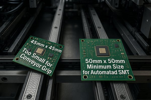
The 50mm x 50mm rule is a safe harbor, based on the physical constraints defined in standards like SMEMA 98511 that govern PCB transport systems. However, an expert engineer knows the exceptions. Some assembly houses can handle smaller boards using specialized pallets or carriers, but this is always a trade-off. It involves a Non-Recurring Engineering (NRE)2 charge for the custom fixture and can increase cycle time, as boards must be manually loaded and unloaded from the carrier. Unless your design absolutely forbids it, panelizing is the superior solution.
How SMT Machine Conveyors Determine Minimum PCB Size
Every machine in an SMT line uses a conveyor with rails that clamp the board edges.
- Minimum Rail Width: Most conveyors cannot close to a gap smaller than 50mm. Trying to feed a 30mm board through is impossible without a carrier.
- Edge Clearance: Machines require a 3mm to 5mm "keep-out" area on the edges they grip. On a small board, this can represent a significant portion of the total real estate, forcing a panelized design.
Why Material Stability and Warpage Also Dictate Minimum Size
The physical stability of the board is just as important as its dimensions.
- Thickness Impact: A very thin board (e.g., 0.6mm or less) is highly susceptible to sagging and warping during reflow, even if its dimensions are larger than 50x50mm. Panelizing with a robust frame provides the rigidity needed to keep the board flat and ensure a reliable soldering process.
- Processable Area: Think in terms of a stable "processable area" rather than just board dimensions. A panel creates a large, stable area that behaves predictably in every machine, which is fundamental to process control.
What Are the Main Reasons for Panelizing Small PCBs?
Is panelizing just another annoying step, or does it offer real benefits? Ignoring it can lead to higher costs, lower quality, and slower production. The reasons for panelization boil down to three things.
Panelization is essential for manufacturing efficiency, cost reduction, and process control. It enables automated handling, drastically cuts down on machine time, and provides the real estate for test features that guarantee quality.
Throughout my career, I've had to justify every design decision. Panelization is one of the easiest to defend because its benefits are so clear and impactful. Let's explore the key drivers in more detail.
Reason 1: Panelization Boosts Manufacturing Throughput
By creating a larger panel, you optimize every step of the automated line. This directly increases throughput, measured in Units Per Hour (UPH). A single panel containing 20 boards that runs through the line in 60 seconds yields a UPH of 1200. Assembling those boards individually might take 15 seconds each, yielding a UPH of only 240, an 80% reduction in efficiency.
Reason 2: Panelization Reduces Per-Unit Assembly Costs
The primary cost driver in SMT assembly is machine time. Panelization attacks this on multiple fronts:
- Stencil Cost: You need one stencil per panel, not one per board. For a panel of 20 boards, this is a 95% reduction in stencil costs.
- Machine Programming: The pick-and-place machine is programmed once for the panel array.
- Reduced Handling: The cost savings from reducing handling operations by 90% or more (as shown in the later cost analysis) cannot be overstated.
Reason 3: Panelization Enables Better Process Control and Quality Assurance
This is what separates a basic understanding from an expert one. The panel's tooling rails are not just waste material; they are valuable real estate for quality assurance.
- Test Coupons: You can add impedance test coupons to the rails. These allow the fabricator to verify that your high-speed trace impedances (e.g., 50-ohm single-ended, 100-ohm differential) are within spec.
- Destructive Testing: A coupon can be cut from the panel and cross-sectioned to verify via plating thickness and dielectric spacing without having to sacrifice a functional board.
- AOI and Fiducial Targets: The frame provides a stable, consistent location for global fiducials3 and alignment targets for Automated Optical Inspection (AOI)4, leading to more reliable inspection results.
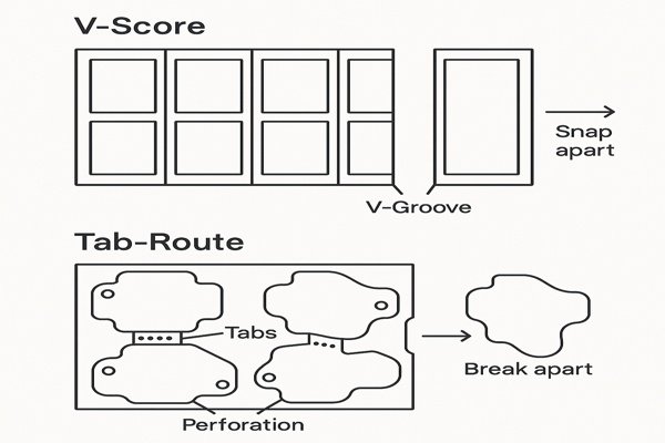
What Is the Difference Between V-Score and Tab-Route Panelization?
You know you need to panelize, but which method should you choose? Using the wrong one can lead to damaged boards, rough edges, or stressed components during separation.
V-scoring (or V-cutting) creates a V-shaped groove along straight lines to separate boards. Tab-routing cuts the board's outline completely, leaving it attached to the frame by small, perforated tabs. The choice depends on board shape, component placement, and your depaneling strategy.
Choosing between these two methods is a critical design decision. Each method has distinct advantages and disadvantages that impact the board's design, cost, and final quality.
Understanding V-Score (or V-Cut) Panelization
This method uses a precision blade to cut a V-shaped groove. The angle of the blade, typically 30 or 45 degrees, impacts the required clearance. A 45-degree blade requires a wider keep-out area on the surface. An advanced technique called "jump scoring" allows the blade to lift and "jump" over a section, leaving parts of the rail intact for improved panel strength.
- Pros: Fast, inexpensive, and produces a clean, straight edge.
- Cons: Only for straight lines. The bending force during separation creates a significant stress zone, making it unsuitable for boards with sensitive components (ceramic capacitors, BGAs, MEMS) near the edge.
Understanding Tab-Route Panelization
This method uses a routing bit to cut the board profile. The router bit diameter (e.g., 1.6mm to 2.4mm) is a trade-off: a smaller bit allows for tighter board spacing but increases machine time and cost.
- Pros: Supports any board shape and allows components right up to the edge. The stress of separation is isolated to the tabs.
- Cons: Slower and more expensive. Leaves rough nubs on the board edge that may require post-processing.
Here’s a summary table to help you decide:
| Feature | V-Score (V-Cut) | Tab-Route |
|---|---|---|
| Board Shape | Rectangular only | Any shape (irregular, curved) |
| Depaneling Method | Manual breaking; pizza-cutter tool | Breaking tabs; automated punch/router |
| Edge Finish | Clean, straight | Rough nubs at tab locations |
| Component Clearance | Required (e.g., >1.27mm from score line) | Not required; can place to edge |
| Stress on Board | High, distributed along the entire edge | Low, concentrated at tabs |
| Cost | Lower | Higher |
| Ideal Use Case | Arrays of identical rectangular boards with no sensitive edge components | Boards with complex shapes or edge-mounted connectors |
What are the Criteria for Choosing Between V-Scoring and Tab-Routing?
Making the wrong panelization choice can break sensitive components or ruin your board's edge finish. How do you decide with confidence? It comes down to a few simple questions about your design.
Choose V-scoring for rectangular boards where you can keep components away from the edges. Choose tab-routing for non-rectangular boards, designs with edge-hanging components, or when placing parts very close to the board edge is unavoidable. For complex designs, consider a hybrid approach.
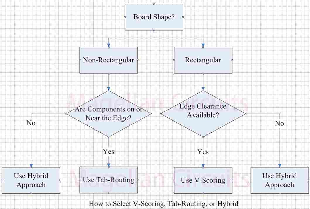
The decision between these two methods is a trade-off between cost, design freedom, and mechanical stress. Use the table below as a quick decision matrix.
| Decision Criterion | Choose V-Score If... | Choose Tab-Route If... |
|---|---|---|
| Board Shape | Your board is a perfect rectangle. | Your board has curves, cutouts, or is non-rectangular. |
| Component Proximity | You can keep all components >1.27mm away from the board edge. | Components must be at or hang over the board edge. |
| Edge Finish | A clean, smooth edge is required. | Minor rough nubs on the edge are acceptable. |
| Depaneling Strategy | You are using manual breaking or a pizza-cutter tool. | You need to support automated routing or punch-based depaneling. |
Choosing Based on Board Shape and Component Placement
This is the primary driver. If the board isn't rectangular or has components that hang over the edge (like some USB connectors), tab-routing is your only option. If you have sensitive components like large BGAs or ceramic capacitors, the stress from V-score depaneling is a significant risk. Tab-routing isolates this stress to the disposable tab.
Choosing Based on Your Depaneling Method and Production Volume
How will the boards be separated? For high-volume production, automated depaneling is used. V-Scoring is best suited for manual breaking or linear cutting machines, while Tab-Routing is essential for robotic routing or punch-based systems that require a fixture.
Choosing Based on Final Board Edge Finish Requirements
How clean does the final board edge need to be? V-scoring provides a cleaner edge. The nubs from tab-routing can interfere with mechanical enclosures and may require manual sanding, adding a costly step to production.
Using a Hybrid Approach: Combining V-Score and Tab-Routing
For complex boards, you don't have to choose just one. An advanced strategy is to use V-scores for the long, straight edges of a board and then use tab-routing to create complex shapes or notches in other areas. This hybrid approach balances cost and design freedom but requires clear communication with your fabricator.
What is the Process for Adding Fiducial Markers to a PCB Panel?
Without proper alignment markers, an automated pick-and-place machine is blind. Forgetting them can render your entire panel useless for assembly, wasting both time and money.
Adding fiducial markers involves placing at least three circular copper pads on the tooling rails of the panel. These markers, designed to a specific standard, allow the machine's vision system to precisely locate the panel and compensate for any rotational or scaling errors.
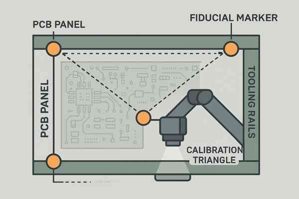
Fiducial markers are the single most important feature for ensuring automated assembly accuracy. Here is the standard process.
Step 1: Designing a Standard Fiducial Marker
According to IPC-7351B5, a fiducial should be a solid circle of exposed metal. Common errors like placing silkscreen over a fiducial or having poor contrast between the pad and the surrounding area can make it unrecognizable to the vision system.
| Fiducial Parameter | IPC-7351B Recommendation | Rationale / Why it Matters |
|---|---|---|
| Shape | Solid filled circle. | Provides a clear, unambiguous target for machine vision systems. |
| Pad Diameter | 1.0mm to 1.5mm (1.0mm is common). | Large enough for reliable detection without consuming excessive space. |
| Solder Mask Clearance | Minimum 2x the pad diameter. | Creates a high-contrast zone, preventing reflection from the mask. |
| Surface Finish6 | Same as the rest of the PCB (e.g., ENIG, HASL). | Ensures a flat, non-oxidized surface for optimal recognition. |
Step 2: Placing Global Fiducials Using a Three-Point System
For panel-level alignment, you must use a three-point system to correct for X, Y, and rotational (theta) errors.
- Placement: Place three fiducials on the tooling strips, as far apart as possible, in an "L" shape.
- Arrangement: One fiducial near the panel's origin (0,0), a second along the X-axis, and the third along the Y-axis. This asymmetry ensures the machine can't mistake the panel's orientation.
Step 3 (Optional): Adding Local Fiducials for High-Precision Boards
For boards with very fine-pitch components (≤0.4mm pitch) or large BGAs, two local fiducials placed on opposite corners of the individual PCB are recommended. This allows the machine to perform a secondary alignment, correcting for any minor placement variation within the panel itself.
What are Tooling Holes and Why are they Needed on a Panel Frame?
You see holes on the edges of every PCB panel, but what are they for? Omitting them or making them the wrong size can prevent your board from being fixtured correctly for testing and assembly.
Tooling holes are non-plated holes placed on the panel's frame that are used for precise mechanical alignment. They secure the panel onto pins in various machines, ensuring absolute positioning during solder printing, assembly, and in-circuit testing.
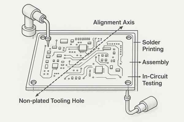
While fiducials provide optical alignment, tooling holes provide robust mechanical alignment. They are essential for processes where physical force is applied or where absolute positional accuracy is critical.
The Key Functions of Tooling Holes in Manufacturing
- Solder Paste Printing: Pins engage the tooling holes to perfectly align the panel with the stencil. Any misalignment here is a primary cause of solder defects.
- In-Circuit Testing (ICT)7: A "bed-of-nails" tester uses tooling pins to clamp the panel, ensuring that hundreds of test probes make reliable contact.
- Fixturing: They are used for holding the panel in automated depaneling systems, programming jigs, and conformal coating frames.
Best Practices for Designing Panel Tooling Holes
- Diameter and Tolerance: The most common size is 3.0mm. A typical fabrication tolerance is ±0.05mm. This tight tolerance is critical for proper fixture fit.
- Type: They must be Non-Plated Through-Holes (NPTH). Plating would alter the diameter unpredictably.
- Advanced Practice - Slotted Holes: To prevent over-constraining the panel and accommodate minor fabrication variances, a best practice is to use one round hole as the primary datum and make the other two tooling holes slotted (e.g., 3mm x 5mm). This provides precise alignment without mechanical stress.
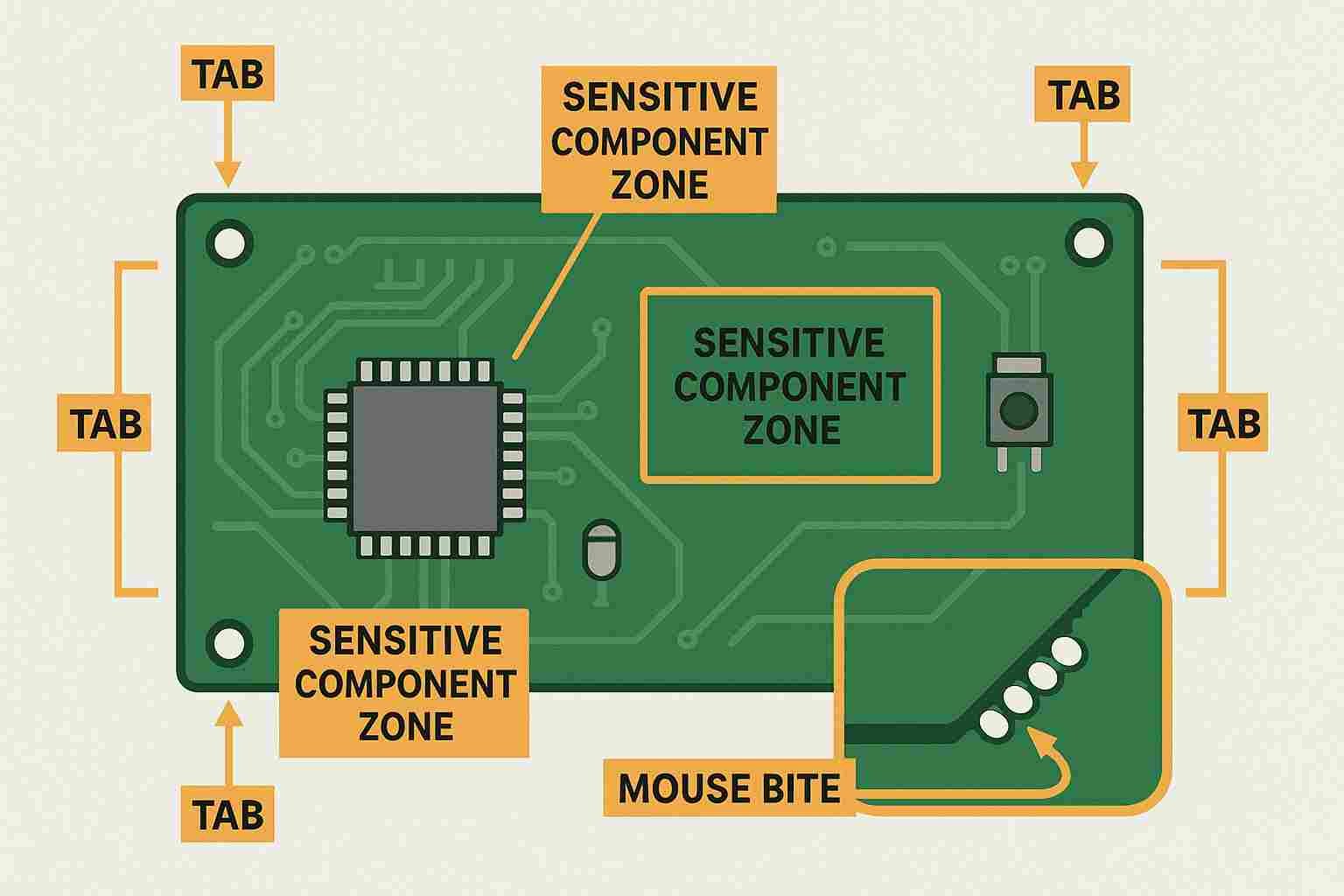
What are "Mouse Bites" in the Context of PCB Panelization?
How do you cleanly separate a tab-routed board without special tools? The secret is in the "mouse bites," but designing them incorrectly can leave jagged edges or make the board impossible to break away.
"Mouse bites" are a series of small, non-plated holes drilled into a breakaway tab to weaken it. This controlled perforation allows an operator to easily and cleanly snap the finished PCB from its manufacturing panel by hand, without damaging the board itself.
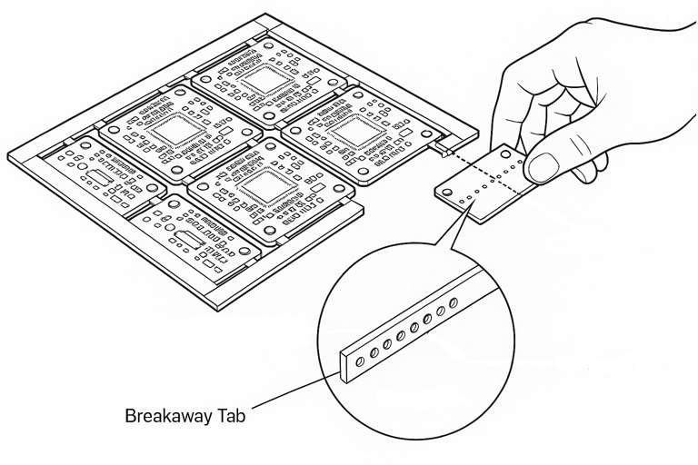
The term "mouse bites" is industry jargon for perforated tabs. A solid tab would be too strong to break, while a tab that is too weak might break during assembly. Mouse bites provide the perfect balance.
How Mouse Bites Enable Clean Board Separation
The goal is a clean snap, not a ragged tear. The remaining nub height will be roughly half the distance between the edges of adjacent holes, so tighter spacing gives a cleaner edge.
Design Specifications for Reliable Mouse Bites
| Parameter | Typical Value | Reason |
|---|---|---|
| Hole Diameter | 0.5mm (20 mils) | Large enough to weaken, small enough for a clean break. |
| Hole Spacing | 0.75mm (30 mils) | Tighter spacing results in a smaller, cleaner nub after separation. |
| Number of Holes | 3 to 5 per tab | Balances strength with ease of breaking. |
| Hole Type | Non-Plated (NPTH) | Plating strengthens the hole, defeating its purpose. |
What are the Best Practices for Designing Breakaway Tabs?
A poorly placed tab can make your board impossible to depanel or, worse, cause it to break during assembly. Designing robust yet functional tabs is a crucial skill for any hardware engineer.
Best practices for breakaway tabs include using 3-5 tabs per board, placing them on straight edges, keeping them away from sensitive components and connectors, and using well-designed mouse bites to ensure a clean, low-stress break.
Breakaway tabs are the critical link between your individual PCB and the manufacturing panel. They need to be strong enough to withstand the entire assembly process but weak enough to be removed easily and cleanly afterward.
| Practice Area | Recommendation | Rationale / Why it Matters |
|---|---|---|
| Quantity & Placement | Use 3-5 tabs, distributed evenly around the board's perimeter. | Provides balanced support, preventing panel sag and vibration during assembly. |
| Dimensions & Strength | Use tabs 2-5mm wide and always perforate with mouse bites. | Ensures the tab is strong enough for handling but weak enough to break cleanly. |
| Component Clearance | Maintain a >2.5mm keep-out between tabs and sensitive components. | The shock of separation can crack ceramic capacitors or damage fine-pitch solder joints. |
| Connector Proximity | Never place tabs next to connectors or mating edges. | The remaining nub can interfere with mechanical assembly or connection points. |
How Does Panelizing Small PCBs Affect the Final Per-Unit Cost?
You assume panelization adds cost, but does it? The answer is nuanced, and getting it wrong can lead you to make poor financial decisions for your project.
Panelization slightly increases the bare board fabrication cost due to wasted material in the frame. However, it dramatically reduces the SMT assembly cost per unit, often by 50-80%, resulting in a significantly lower total cost for the final assembled product.
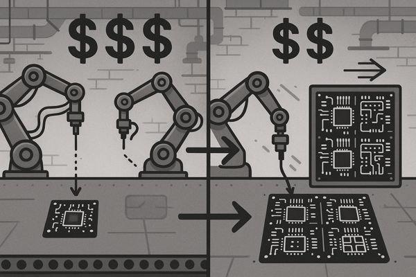
As an engineer responsible for project budgets, I constantly analyze the cost impact of my design choices. Panelization is a perfect example of where a small upfront "cost" leads to massive downstream savings.
Analyzing the Cost Impact: Fabrication vs. Assembly Costs
Let's use our example of 1,000 units of a 25mm x 40mm PCB.
- Fabrication Cost: Your panel design's efficiency matters. Fabs fit your panels onto their large production panels (e.g., 18" x 24"). If your panel wastes space, your cost increases. By fitting 20 boards on an optimized 150mm x 220mm panel, the per-unit bare board cost is $0.30.
- Assembly Cost: The savings here are immense. We only load 50 panels, not 1,000 boards. This reduction in handling and machine setup brings the per-unit assembly cost down to ~$0.60.
- Total Cost: The panelized total cost is $0.90 per unit, a 72% saving compared to the hypothetical non-panelized cost of $3.20.
| Cost Factor | Scenario A: Individual Board | Scenario B: Panelized Board | Result |
|---|---|---|---|
| Bare Board (Fab) | $0.20 | $0.30 | Panelizing is 50% more expensive |
| Assembly | $3.00 (avg.) | $0.60 (avg.) | Panelizing is 80% cheaper |
| Total Per Unit | $3.20 | $0.90 | Panelizing saves ~72% |
Is it Possible to Place Different PCB Designs on a Single Panel?
Have several small projects ready for prototyping? You might be wondering if you can save money by combining them onto a single manufacturing panel instead of ordering them all separately.
Yes, it is possible to place multiple different PCB designs on a single panel. This practice, often called "multi-design panelization," is common for prototyping to save on setup costs, but all boards on the panel must share the exact same layer stack-up, thickness, and material.
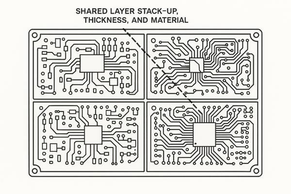
I've used multi-design panels many times for R&D. However, there are important constraints to be aware of.
Fabrication Constraints for Multi-Design Panels
All boards on the panel must be identical in their core construction: same layer count, stack-up, material, copper weight, and surface finish. There are no exceptions.
Assembly and Production Challenges with Multi-Design Panels
This is where it gets tricky. If one board is single-sided and another is double-sided, the panel will require two separate, complex assembly runs, completely negating any cost savings. For production, it's generally a bad idea due to inventory mismatch problems. An exception is a "family panel," where related boards (e.g., a main board and its required daughterboard) are intentionally kept together for a single product assembly.
What are the Typical Requirements for Submitting a Panelized Design to a Fabricator?
You've finished your panel layout. What exactly do you need to send to the manufacturer to ensure they build it correctly and avoid a round of confusing questions?
To submit a panelized design, you must provide a complete file package that includes Gerber files for each layer, Excellon drill files, and a detailed fabrication drawing. For maximum clarity, also include a README file and consider using modern formats like IPC-2581.
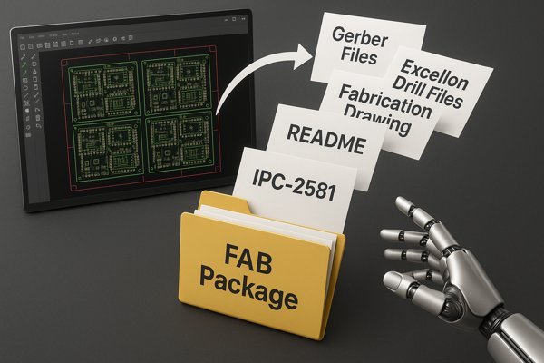
From my experience working with dozens of fabricators globally, clear and complete documentation is the number one factor in preventing manufacturing errors.
| File / Document | Key Contents & Requirements | Purpose / Why it's Needed |
|---|---|---|
| Gerber Files (RS-274X) | All copper, solder mask, silkscreen, and paste layers. | Defines the artwork for each physical layer of the board. |
| Excellon Drill Files | Separate PTH (plated) and NPTH (non-plated) files. | Specifies the location, size, and type of every hole to be drilled. |
| Fabrication Drawing | Panel dimensions, layer stack-up, V-score/tab details, special notes. | The primary human-readable instruction manual for the CAM engineer. |
| README.txt File | File naming conventions, special instructions, contact info. | Resolves ambiguity and prevents common errors in interpretation. |
| IPC-25818 (Optional) | An all-in-one file containing stack-up, layers, drill, and BOM data. | A modern standard that reduces risk by combining all data into one file. |
Conclusion
In short, panelization isn't an optional step for small PCBs; it's a fundamental requirement for efficient, cost-effective, and high-quality automated manufacturing. Master it, and you'll avoid major production headaches.
-
Understanding SMEMA 9851 is crucial for optimizing PCB transport systems and ensuring compliance with industry standards. ↩
-
Exploring NRE charges can help you make informed decisions about custom fixtures and their implications on project costs. ↩
-
Learn how fiducials improve PCB assembly accuracy and why they're essential for reliable automated optical inspection and alignment during manufacturing. ↩
-
Learn how AOI technology detects defects in PCB assembly, ensuring higher quality and reliability for your electronic products. ↩
-
Exploring IPC-7351B guidelines will provide you with essential standards for designing effective fiducial markers. ↩
-
Learn about various PCB surface finishes like ENIG and HASL to choose the best option for optimal fiducial recognition and board reliability. ↩
-
Learn how In-Circuit Testing (ICT) ensures PCB quality by detecting assembly defects and why it's a crucial step in electronics manufacturing. ↩
-
Learn how IPC-2581 streamlines PCB data exchange, reduces errors, and why it's becoming the preferred standard for modern electronics manufacturing. ↩


