 Skip to content
Struggling with dense PCB designs? Wondering if via-in-pad is a risky choice for manufacturing? Let's clear up the confusion.
Via-in-pad isn't inherently bad for manufacturing. It offers density benefits but requires careful design and a capable fabricator to avoid potential yield issues and higher costs. When properly implemented, it's a reliable solution.

Many engineers I've talked to hesitate when via-in-pad (VIP) comes up. They've heard stories, seen the increased costs, and wonder if it's worth the potential headaches. But like any advanced technique, understanding its nuances is key. Let's dive deeper into what via-in-pad really means for your design and your manufacturing partner, exploring its benefits, challenges, and how to get it right.
What Is Via-In-Pad Technology in PCB Design?
Confused by PCB jargon? "Via-in-pad" sounds complex, but its purpose is simple. Understand this key technology for modern electronics.
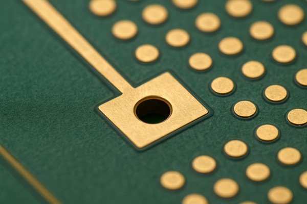
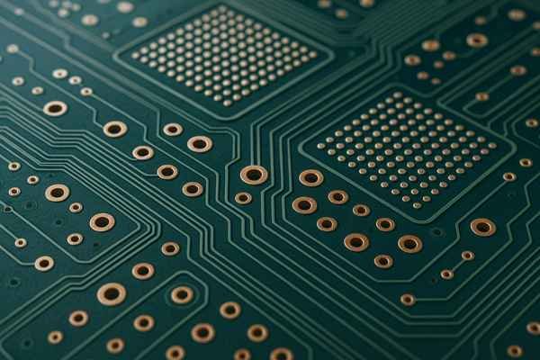
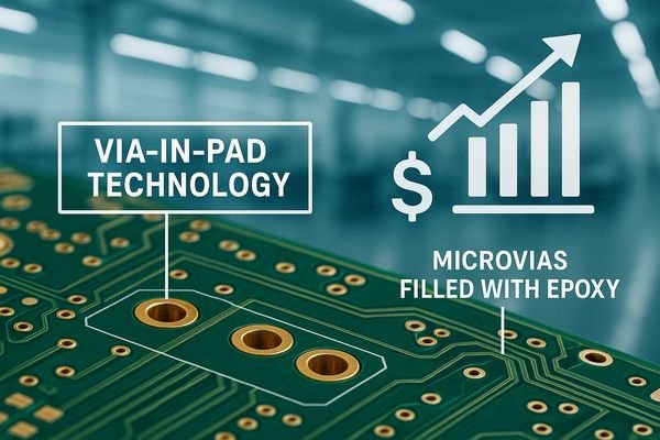
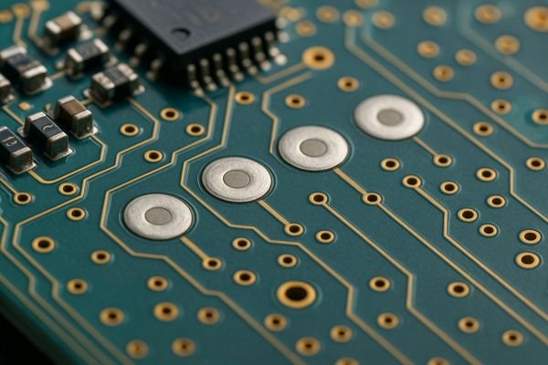
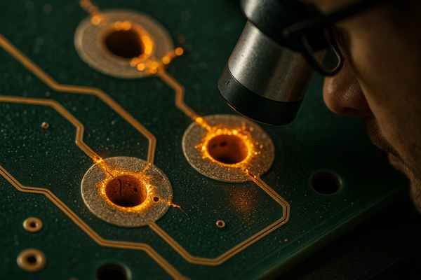
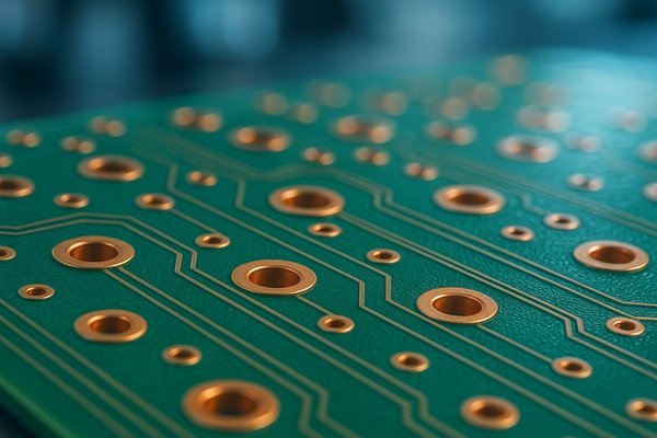
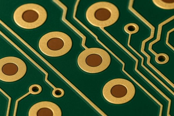
Via-in-pad (VIP) technology places the via directly beneath a component's solder pad. This contrasts with traditional vias, which are offset and connected by a short trace (dog-bone), saving space and shortening signal paths.
Understanding the Fundamentals of Via-In-Pad
Via-in-pad essentially means that the hole for the via is drilled directly into the surface mount technology (SMT) pad. This is different from the conventional method where a via, often called a "dog-bone" via, is placed near the SMT pad and connected with a small trace.
Key Characteristics of VIP
The primary goals of using via-in-pad are to save valuable PCB real estate and to shorten electrical signal paths. I remember a project with a particularly tight BGA; we simply couldn't route all the signals out using traditional dog-bone vias. The design team was stuck until we decided to explore via-in-pad. It was a learning curve, but essential for that product's form factor.
Ensuring Reliability
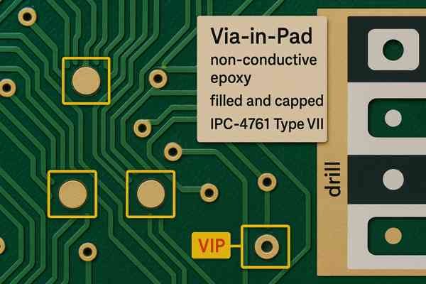
To ensure reliability, these vias usually need to be filled and made planar. According to IPC-47611, "Design Guide for Protection of Printed Board Via Structures," Type VII (Filled and Capped Via) is the typical structure recommended for via-in-pad applications to ensure a solderable and reliable surface.
| Feature | Via-in-Pad (VIP) | Traditional Via (e.g., Dog-bone) |
|---|---|---|
| Location | Directly under the SMT pad | Offset from the SMT pad |
| Connection | Integral to pad | Connected by a short trace |
| Space Usage | Minimal | Requires extra space for via & trace |
| Signal Path | Shortest possible | Longer due to trace |
| Complexity | Higher (filling, planarizing, capping) | Lower |
What Are the Advantages of Using Via-In-Pad?
Need to shrink your PCB size? Or improve high-speed signal performance? Via-in-pad might be the solution you're looking for.
Key advantages of via-in-pad include increased component density, shorter signal paths for better integrity, improved thermal management by conducting heat away, and simplified routing for fine-pitch components like BGAs and QFNs.
Key Benefits of Adopting Via-In-Pad
The advantages of via-in-pad are quite significant in modern electronics, addressing several key design challenges.
Density Enhancements
VIP allows for increased component density because you don't need extra space next to the pad for a separate via and trace. This is crucial for miniaturization and fitting more functionality into smaller form factors.
Signal Integrity Benefits
VIP leads to improved signal integrity. Shorter trace lengths directly translate to lower parasitic inductance and capacitance. For instance, reducing trace length by even a few millimeters can impact signals operating above 1 GHz by minimizing unwanted impedance variations and signal reflections.
Thermal Performance Gains
Via-in-pad can offer better thermal management. The vias act as direct thermal conduits, drawing heat from the component down to internal copper planes or to the other side of the board. An array of them under a thermal pad can significantly improve heat dissipation.
Routing Simplification
Lastly, it greatly simplifies routing, especially for components with very fine pitches, like 0.5mm or 0.4mm BGAs, making it easier to escape inner rows of connections.
| Advantage | Description | Impact Area |
|---|---|---|
| Increased Component Density | Vias are under pads, saving space. | Miniaturization |
| Improved Signal Integrity | Shorter signal paths reduce parasitics (L, C). | High-Speed Design |
| Better Thermal Management | Vias conduct heat away from components. | Power, Heat Diss. |
| Simplified Routing | Easier fan-out for fine-pitch components (BGAs, QFNs). | Complex Layouts |
How Does Via-In-Pad Help With BGA/QFN Routing?
Struggling to fan out signals from dense BGAs or QFNs? Traditional methods failing? Via-in-pad offers a direct escape route.
Via-in-pad allows vias to be placed directly on BGA/QFN pads, enabling direct signal escape to inner layers. This eliminates complex dog-bone fanouts, simplifying routing for fine-pitch (e.g., ≤ 0.5mm) components.
Solving Complex Routing Challenges for Fine-Pitch ICs
Routing fine-pitch Ball Grid Arrays (BGAs) and Quad Flat No-leads (QFNs) is a common and often significant challenge in modern PCB design.
The Fine-Pitch Challenge
The table below illustrates how decreasing BGA pitch makes traditional fanout methods increasingly difficult, highlighting the need for VIP.
| BGA Pitch | Typical Pad Diameter | Approx. Space Between Pads (Edge-to-Edge for 0.1mm trace/space) | Feasibility of Dogbone (Trace + Via) | VIP Advantage |
|---|---|---|---|---|
| 0.8mm | ~0.40mm | ~0.3mm - 0.4mm | Usually Feasible | Optional, for density or shorter paths |
| 0.65mm | ~0.30mm | ~0.25mm - 0.35mm | Challenging | Increasingly beneficial for clean routing |
| 0.5mm | ~0.25mm | ~0.15mm - 0.25mm | Very Challenging / Often Impossible | Often Necessary for fanout |
| 0.4mm | ~0.20mm | ~0.10mm - 0.20mm | Generally Impossible with std. rules | Essential for fanout of inner rows |
(Note: Feasibility depends on specific design rules, via size, and trace width.)
VIP as a Direct Escape
Via-in-pad solves this elegantly by allowing the via to be placed directly under the BGA ball's pad, so the signal can drop straight down to an inner routing layer. This frees valuable space on outer layers. I worked on a medical device with a 0.4mm pitch BGA that had hundreds of connections. Without via-in-pad, we would have needed at least two more layers and a larger BGA footprint.
Impact on Decoupling
This direct downward path is also highly beneficial for placing bypass capacitors very close to BGA power pins, often on the reverse side of the board, which minimizes inductance for better power delivery.
When Is Via-In-Pad Necessary or Recommended?
Wondering if your design really needs via-in-pad? Is it an essential upgrade or an unnecessary expense? Let's clarify when to use it.
Via-in-pad is necessary for designs with very high-density interconnects (HDI), fine-pitch BGAs (typically 0.5mm pitch or smaller), or when minimizing signal path lengths for high-speed signals is critical for performance.
Identifying Optimal Use Cases for Via-In-Pad
Via-in-pad isn't a technique to be used casually due to its added cost and complexity. However, there are definite scenarios where its benefits outweigh these drawbacks.
Key Application Drivers
The most common drivers include:
- Fine-Pitch Components: For BGAs with pitches of 0.5mm, and especially for 0.4mm or 0.3mm, routing without VIP is often impractical.
- High-Density Interconnect (HDI) Designs: Where every fraction of a millimeter of board space is critical.
- High-Speed Signal Integrity2: When minimizing trace length (e.g., by 50-100 mils or 1.27-2.54 mm) is crucial for interfaces like DDR memory or RF circuits.
- Thermal Management: For placing thermal vias directly under component thermal pads to improve heat dissipation.
Balancing Benefits and Costs
I always advise engineers: if you can reliably route your board and meet all performance requirements with traditional vias without excessively increasing layer count or board size, stick with that. Use VIP when the benefits clearly justify the added manufacturing steps.
| Scenario | VIP Recommendation | Justification |
|---|---|---|
| BGA Pitch > 0.65mm, ample routing space | Not usually recommended | Traditional vias are more cost-effective. |
| BGA Pitch 0.5mm - 0.65mm | Optional / Recommended | Depends on routing density and layer count targets. |
| BGA Pitch ≤ 0.5mm | Often Necessary / Highly Recommended | Extremely difficult or impossible to route without VIP. |
| High-Speed Signals (e.g., >3 Gbps) | Recommended for critical nets | Minimizes parasitic inductance/capacitance for better signal integrity. |
| High Power Density / Thermal Pads | Recommended for thermal vias under pads | Improves heat dissipation directly from the component. |
What Are the Common Manufacturing Problems With Via-In-Pad?
Worried about manufacturing issues with via-in-pad? Heard horror stories of bad yields? Understand the common pitfalls to avoid them.
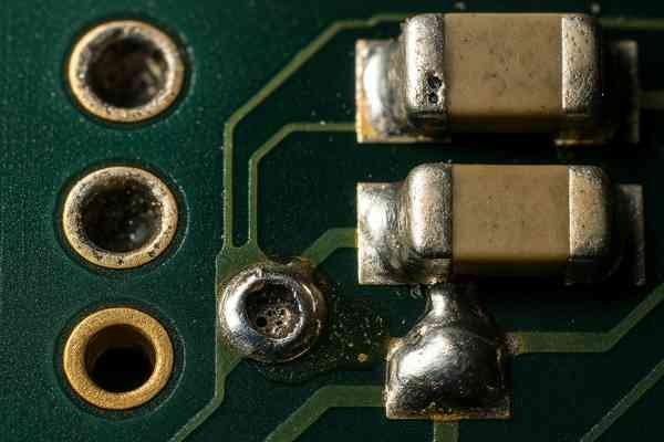
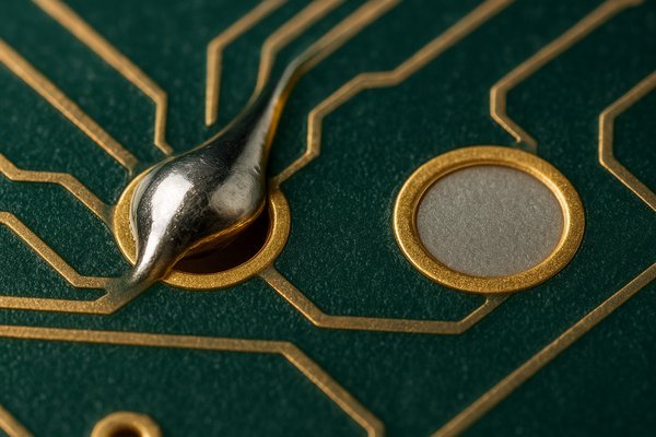
Common manufacturing problems include solder wicking into the via (creating voids or insufficient solder on the pad), trapped flux/air leading to outgassing, and non-planar pads affecting component placement and solder joint reliability.
While beneficial, via-in-pad technology comes with its share of potential manufacturing headaches if not managed properly by both the designer and the fabricator.
Solder-Related Defects
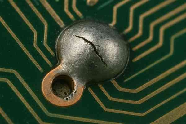
Solder wicking is a prime concern: molten solder flows into an improperly filled via, leaving insufficient solder for the joint. Voids in the solder joint can also occur due to outgassing from trapped flux or air if the via isn't perfectly sealed.
Structural and Planarity Issues
A non-planar surface on the pad is a major problem. If the filled and capped via creates a bump or a dimple (deviations greater than, say, 25-50 µm or 1-2 mils can be problematic for fine-pitch BGAs), components may tilt. IPC-A-610 ("Acceptability of Electronic Assemblies") has strict criteria for solder joints. I’ve seen batches of boards fail because the via filling process wasn't adequately controlled, leading to BGA coplanarity issues and intermittent connections. Incomplete filling can also lead to structural weaknesses.
| Problem | Potential Cause | Consequence |
|---|---|---|
| Solder Wicking | Incompletely filled/sealed via | Insufficient solder on pad, open/weak joints |
| Solder Joint Voids | Outgassing from trapped air/flux in via | Reduced joint strength, potential for cracks |
| Non-Planar Pad Surface | Improper via fill/planarization, uneven capping | Tilted components, uneven BGA collapse, opens/shorts |
| Incomplete Via Fill | Poor fill process control, high aspect ratio vias | Voids in fill, potential for outgassing, solder wicking |
| Trapped Plating Chemicals | Improperly sealed via before final plating steps | Long-term reliability issues, corrosion |
How Does Via-In-Pad Affect PCB Fabrication Costs?
Considering via-in-pad but worried about the budget? How much extra does this advanced technology really cost? Let's break it down.
Via-in-pad significantly increases PCB fabrication costs due to additional process steps like via filling (conductive or non-conductive epoxy) and planarization. Expect costs to be 15-30% higher, sometimes more, depending on complexity.
Analyzing the Cost Implications of Via-In-Pad
There's no denying that via-in-pad adds to the cost of PCB fabrication. This isn't arbitrary; it's due to the extra materials and processing steps involved.
Primary Cost Drivers
The following table outlines the main process steps unique to VIP that contribute to its higher cost:
| Cost Driver Component | Description | Estimated % Impact on Overall VIP Cost Adder (Illustrative) |
|---|---|---|
| Via Filling (Non-Conductive) | Epoxy material cost, screen/dispense setup, application labor/machine time | 25-40% |
| Via Filling (Conductive) | Higher material cost (e.g., silver epoxy), similar application process | Adds 50-100%+ to fill material cost vs. non-conductive |
| Planarization | Grinding/lapping machine time, labor, consumables, cleaning | 20-35% |
| Capping | Additional copper plating step, surface preparation | 10-20% |
| Increased Process Control | Tighter tolerances, more inspection points, specialized handling | 5-15% |
| Potential Yield Impact | Factored into overall pricing by experienced fabs | (Embedded in overall premium) |
(Note: Percentages are illustrative contributions to the additional cost of VIP, not the total board cost.)
Estimating the Cost Premium
As a general guideline, a board with non-conductive epoxy-filled and capped via-in-pad might cost approximately 15% to 30% more than an equivalent board without VIP. For very complex HDI boards with multiple layers of VIPs, this premium can be higher. For example, if a standard prototype run costs $200, a VIP version could range from $230 to $260 or more. This is a significant factor for cost-sensitive projects and needs to be justified by the design requirements.
What Are the Yield Implications of Using Via-In-Pad?
Adopting via-in-pad but anxious about production yields? Will this choice lead to more failed boards? Understand the risks and mitigations.
Using via-in-pad can potentially lower manufacturing yields if not implemented with precision. Issues like incomplete via filling, poor planarization, or solder wicking can lead to assembly defects and board failures if the fabricator isn't experienced.
Understanding and Mitigating Yield Risks
Yield is a critical metric, and via-in-pad (VIP) can indeed introduce factors that affect it, particularly if processes are not mature or well-controlled.
Factors Influencing VIP Yield
The primary yield detractors relate to the quality of the via fill and subsequent planarization and capping. The table below highlights common issues and mitigation approaches:
| Yield Detractor | Common Cause | Mitigation Strategy |
|---|---|---|
| Incomplete Via Fill / Voids | High aspect ratio, improper fill process/material, air trap | Optimize aspect ratio, vacuum-assisted fill, appropriate fill material, SPC |
| Poor Pad Planarity | Incorrect grinding/lapping, uneven fill cure, cap issues | Strict process control, calibrated equipment, in-process inspection (e.g., profilometry) |
| Solder Wicking (at assembly) | Unfilled/improperly capped vias, surface voids in fill | Adherence to IPC-4761 Type VII, 100% fill & cap integrity checks where critical |
| Via-to-Pad Misregistration | Poor drill/imaging accuracy, material instability | High-precision equipment, fab DFM checks, stable materials |
| Contamination / Residues | Insufficient cleaning before/after fill, trapped chemicals | Stringent cleaning protocols, controlled environment, proper curing/sealing |
| Cracking/Delamination of Cap | Poor plating adhesion, excessive stress, fill CTE mismatch | Material selection, robust plating process, stress testing qualification |
Working with Your Fabricator
I recall a project ramp-up where our initial assembly yield with a new VIP design was around 85%, far from our target of 98%. We had to collaborate closely with the PCB fabricator to fine-tune their via fill (type of epoxy, application method) and planarization process (grinding pressure, pad material) specifically for our design's via sizes (0.25mm) and pad geometries. It took several iterations and careful process validation, including cross-sectioning samples from each batch, to hit our yield targets. A good fabricator will have robust statistical process control (SPC) for these critical steps.
What Is Solder Wicking in Via-In-Pad and How to Prevent It?
Seeing solder disappear into vias during assembly? This "wicking" can starve your joints. Learn how to prevent this common via-in-pad problem.
Solder wicking is when molten solder flows down into the via barrel instead of forming a proper joint on the pad. It's primarily prevented by completely filling the via with epoxy and then plating over it (capping).
Addressing Solder Wicking: Causes and Solutions
Solder wicking is a notorious issue if via-in-pad structures are not correctly manufactured.
Understanding the Mechanism
During solder reflow, the molten solder on the pad is subject to capillary action. If there's an open pathway or void within the via barrel connected to the pad, the solder will preferentially flow down into this opening, away from the intended solder joint area.
Consequences of Wicking
This leaves an insufficient amount of solder on the pad surface to form a robust connection with the component lead or BGA ball. The results are predictable: starved or open solder joints, weak or intermittent electrical connections, and reduced mechanical strength. For BGAs, where precise solder volume (typically forming a collapsed sphere of a specific height, e.g., 0.1mm to 0.25mm) is critical, wicking can be disastrous.
Effective Prevention: Filling and Capping
The most effective way to prevent solder wicking is to ensure the via is properly processed. This involves complete filling of the via with a suitable material (typically non-conductive epoxy) and then capping (plating copper over) the filled via, as detailed in IPC-4761 Type VII. The following table outlines key practices:
| Do's for Preventing Solder Wicking | Don'ts for Preventing Solder Wicking |
|---|---|
| Specify IPC-4761 Type VII (Filled & Capped) | Assume basic via plugging is sufficient for VIP pads |
| Ensure >95% via fill is specified & verified | Use open/unfilled vias directly under SMT pads |
| Require planarization after fill & cap | Overlook surface finish compatibility with the cap |
| Verify fabricator's VIP capabilities | Ignore fabricator DFM feedback on via structures |
| Inspect for complete capping over filled area | Allow exposed epoxy or voids at the pad surface |
I've seen a contract manufacturer mistakenly skip the via filling step on prototypes. During BGA reflow, most solder for pads with vias wicked down, rendering the boards useless.
Are There Reliability Concerns With Via-In-Pad Technology?
Worried about the long-term reliability of via-in-pad? Could these tiny structures fail over time? Let's address the concerns.
Reliability concerns with via-in-pad can arise if poorly executed. Issues include voids in the via fill leading to outgassing or stress points, and potential for solder joint fatigue if not designed for thermal cycling.
Assessing Long-Term Reliability of Via-In-Pad
When manufactured correctly by a capable fabricator adhering to industry standards like IPC-6012 Class 2 or 3, via-in-pad (VIP) structures are generally reliable. However, manufacturing defects can introduce long-term risks.
Potential Failure Modes & Mitigations
The table below outlines common reliability concerns associated with VIP structures and how to address them:
| Reliability Concern | Potential Cause(s) | Mitigation Strategy |
|---|---|---|
| Voids in Via Fill | Trapped air/flux during fill, incomplete cure, poor fill flow | Vacuum-assisted filling, optimized fill material & process, proper cure schedule, X-ray inspection |
| Outgassing from Fill | Volatiles in fill material, incomplete cure, moisture ingress | Use low-outgassing fill materials, ensure full cure, proper sealing by cap |
| CTE Mismatch Stress | Differences in expansion between fill, copper, laminate, cap | Select fill materials with compatible CTEs, robust via/cap structure, thermal cycling test |
| Trapped Contaminants | Insufficient cleaning before filling or capping | Stringent multi-stage cleaning protocols, controlled manufacturing environment |
| Cracking of Via/Cap | Excessive stress (thermal/mechanical), poor plating adhesion | DFM for stress relief, material selection, robust plating process, stress testing |
| Electromigration in Fill | (Primarily for conductive fills) Voltage bias, humidity, ions | Use high-purity conductive fills, ensure proper sealing, conformal coating if needed |
Mitigating Reliability Risks
When I qualify a vendor for VIP, I scrutinize their fill process (e.g., vacuum-assisted filling for high aspect ratios), void inspection methods (routine cross-sectioning, X-ray sampling), material datasheets for CTE and Tg, and their historical reliability data (e.g., results from thermal shock testing on similar structures).
Can Via-In-Pad Lead to Solder Joint Fatigue or Failure?
Do via-in-pad designs experience more solder joint failures? What causes this fatigue, and can it be prevented in your critical applications?
Yes, poorly implemented via-in-pad can contribute to solder joint fatigue. This is often due to non-planar pads creating uneven stress, voids in the fill acting as stress concentrators, or significant CTE mismatches under thermal cycling.
Examining Solder Joint Fatigue in VIP Designs
Solder joint fatigue is a concern for all SMT assemblies, especially under harsh thermal cycling or high vibration. Via-in-pad structures can, if not perfectly executed, introduce factors that may accelerate this.
How VIP Can Induce Stress
The primary concern is how the underlying via structure influences stress distribution within the solder joint.
- Non-Planar Pad Surface: If the filled and capped via creates a significant bump or dimple (e.g., > ±25 µm for fine-pitch BGAs), the BGA ball won't sit flat. This leads to an uneven solder joint shape and localized stress concentrations, which are initiation points for fatigue cracks.
- Voids in Via Fill: Voids, especially near the pad surface or via barrel interface, can act as stress risers or allow micro-movements, propagating stress to the solder joint.
Factors Contributing to Fatigue
| Factor | Contribution to Solder Joint Fatigue with VIP | Prevention/Mitigation |
|---|---|---|
| Poor Pad Planarity | Uneven stress distribution in solder joint | Strict planarization process control (e.g., target < ±25µm deviation) |
| Voids in Via Fill | Stress concentration, potential for movement/outgassing | Optimized via fill process, void inspection (X-ray, cross-section) |
| Large CTE Mismatch | Differential expansion/contraction stressing the joint | Selection of appropriate fill materials with compatible CTEs, robust via structure |
| Inadequate Capping | Weak interface between pad and via fill, potential for delamination | Proper cap plating thickness and adhesion |
I recall an automotive product failing thermal shock tests (-40°C to +125°C, 1000 cycles). Cross-sections showed micro-cracks initiating at via-in-pad locations under a large BGA. The issue was traced to inconsistent via filling creating slight doming (around 40-50 µm) on some pads. Improving the filling and planarization process to achieve <20 µm deviation resolved it.
What Types of Via Filling Are Used for Via-In-Pad?
Heard about "filled vias" but unsure what materials are used? Knowing the options is key to a successful via-in-pad design.
Common via filling types for via-in-pad include non-conductive epoxy (most common and cost-effective), conductive epoxy (silver or copper filled for thermal/electrical conductivity), and occasionally specialized copper paste followed by plating for maximum conductivity.
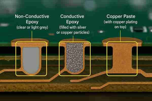
Exploring Via Fill Materials and Their Applications
The choice of via fill material for via-in-pad applications depends on the specific requirements for cost, thermal conductivity, and electrical conductivity.
Common Fill Options
| Fill Type | Material Composition | Typical Thermal Conductivity (W/mK) | Relative Cost | Primary Purpose |
|---|---|---|---|---|
| Non-Conductive Epoxy | Epoxy resin (thermoset) | Low (0.2 - 0.5) | Low | Plugging, planarization, prevent solder wicking |
| Conductive Epoxy (Silver) | Epoxy resin + Silver particles | Medium (2 - 20+) | Medium-High | Thermal/electrical enhancement, plugging, planarization |
| Conductive Epoxy (Copper) | Epoxy resin + Copper particles | Medium (similar to Silver) | Medium-High | Similar to Silver fill, less common |
| Copper Paste / Plated Copper | High copper content paste or plated Cu | High (approaching pure Cu: ~200-380) | High | Maximum thermal/electrical conductivity, plugging |
Choosing the Right Fill
- Non-Conductive Epoxy Fill: This is the workhorse for most VIP applications where the main goal is achieving density, enabling routing, and providing a solderable surface after capping. It's the most cost-effective.
- Conductive Epoxy Fill: Used when improved thermal dissipation through the via is needed (e.g., for thermal pads of QFNs or power devices) or if some level of electrical conductivity through the fill itself is beneficial, though the plated via barrel still carries most current. Silver-filled is common.
- Copper Paste/Plated Copper Fill: Reserved for high-power applications or very demanding thermal management scenarios where maximizing heat transfer through the via is critical. This is the most expensive and complex option.
For most of my standard BGA/QFN designs, non-conductive epoxy fill (IPC-4761 Type VII) is perfectly adequate and balances performance with cost.
Is Via Capping Necessary for Via-In-Pad?
Just filling the via isn't always enough for via-in-pad. Is an extra "capping" step really needed? Understand why it's often crucial.
Yes, via capping (plating copper over the filled via) is highly recommended and generally considered necessary for reliable via-in-pad. It creates a smooth, robust, solderable surface and completely seals the fill material.
The Critical Role of Via Capping
Via capping is an indispensable step in creating a high-quality, reliable via-in-pad structure. It's not just an optional add-on; it's integral to the concept.
The Role of the Copper Cap
After the via hole is filled with epoxy (conductive or non-conductive) and the surface is planarized (made flat), a layer of copper is electroplated over the filled via opening. This copper "cap" forms the actual SMT pad surface. This is why the IPC-4761 Type VII (Filled and Capped Via) structure is the standard specification.
Benefits of Capping
- Solderability: The epoxy fill material itself is typically not directly solderable. The copper cap provides a consistently metallic and solderable surface, compatible with standard solder paste and reflow processes. The final surface finish (e.g., ENIG, OSP, Immersion Silver) is then applied over this cap.
- Planarity: While planarization flattens the fill, the capping process ensures a uniform copper surface across the pad, critical for consistent solder paste deposition and component seating, especially for BGAs.
- Sealing: The copper cap completely seals the fill material within the via. This is crucial to prevent any outgassing from the epoxy during solder reflow (which could cause solder voids) and to protect the fill from absorbing moisture or processing chemicals during assembly or in the product's operational life.
- Reliability & Robustness: The cap creates a more durable pad structure, ensuring a good electrical and mechanical connection between the component, the solder joint, and the plated via barrel. The cap thickness is typically similar to the board's outer layer copper, e.g., 18 µm (0.5 oz) or 35 µm (1 oz).
Omitting the cap would leave the epoxy exposed, leading to severe assembly problems and poor reliability.
What Are the DFM (Design for Manufacturability) Guidelines for Via-In-Pad?
Want to use via-in-pad without manufacturing nightmares? Following Design for Manufacturability (DFM) rules is critical. Learn the key guidelines.
Key DFM guidelines for via-in-pad include specifying via fill type (e.g., non-conductive epoxy) and capping (IPC-4761 Type VII), requiring planarization, defining acceptable via-to-pad registration, and ensuring appropriate via aspect ratios for reliable filling/plating.
Essential DFM Strategies for Via-In-Pad Success
Adhering to Design for Manufacturability (DFM) guidelines is absolutely essential when implementing via-in-pad to ensure good yields, reliability, and reasonable costs.
Key Design Specifications
Your fabrication notes must be unambiguous:
- Via Structure: Explicitly call out "Via-in-Pad structures to be IPC-4761 Type VII (Filled with non-conductive epoxy, planarized, and capped with copper)" or equivalent.
- Planarity: If critical (e.g., for 0.4mm pitch BGAs), specify a planarity tolerance for the capped via surface, such as "Co-planarity of capped via surface with adjacent copper pad to be within ±0.025mm (±1 mil)."
Geometric Considerations
| DFM Aspect | Guideline / Consideration | Why it Matters |
|---|---|---|
| Via Aspect Ratio | Ratio of via depth to drill diameter. For filling, lower is better (e.g., <10:1 for through-vias, <1:1 for microvias). | High aspect ratios are harder to fill completely without voids. |
| Drill Size | Typically 0.15mm to 0.3mm (6 to 12 mils) for VIPs. Consult fab capability. | Affects fill-ability and routing density. |
| Pad Size | Must be large enough to accommodate the via drill, tolerances, and ensure sufficient solderable area after capping. | Reliable soldering and assembly. |
| Annular Ring | Less critical for the "pad" itself if it's fully capped, but registration of drill to eventual cap matters. | Ensures the cap fully covers the filled via. |
Communication with Fabricator
Crucially, discuss your via-in-pad design with your chosen PCB fabricator early in the design process. They will provide their specific capabilities (e.g., minimum drill size for filling, achievable planarity, preferred fill materials). I make it a standard practice to send preliminary stackups and critical component footprints for a DFM review before finalizing the layout. This proactive approach has saved me countless headaches and potential respins.
What Are the Manufacturing Differences Between Via-In-Pad and Traditional Vias (Dog-Bone Fanout)?
Via-in-pad sounds more complex than old-school dog-bone vias. What are the actual extra steps and differences in the factory?
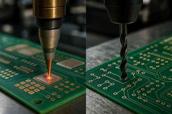
Manufacturing via-in-pad involves several extra steps: precise via drilling, thorough cleaning, specialized epoxy filling, epoxy curing, critical planarization (grinding/sanding), and then copper capping/plating. Traditional vias just require drilling and standard through-hole plating.
Contrasting VIP and Traditional Via Fabrication Processes
The manufacturing processes for via-in-pad (specifically filled and capped, IPC-4761 Type VII) and traditional "dog-bone" vias diverge significantly, explaining the difference in complexity and cost.
Process Flow Comparison
| Process Step | Traditional Via (Dog-Bone) | Via-In-Pad (Filled & Capped) | Notes for VIP |
|---|---|---|---|
| 1. Drilling | Yes (Standard tolerance) | Yes (Often tighter tolerance, smaller drills) | Drill quality is critical. |
| 2. Hole Cleaning/Deburr | Yes | Yes (More critical for good fill adhesion) | |
| 3. Via Barrel Plating (Initial) | Yes (Full PTH process) | Yes (May be thin electroless Cu or full PTH) | Ensures conductivity of via barrel. |
| 4. Via Filling | No | Yes (Epoxy screen print, squeegee, or vacuum) | Additional Step: Key VIP process. |
| 5. Fill Curing | No | Yes (Baking cycle) | Additional Step: Time and energy. |
| 6. Planarization | No | Yes (Grinding, lapping, sanding) | Additional Step: Critical for surface flatness. |
| 7. Surface Prep for Plating | Yes (For outer layers) | Yes (For capping and outer layers) | Ensures good adhesion of the cap. |
| 8. Via Capping / Pad Plating | No (Pad is separate) | Yes (Plate copper over filled via) | Additional Step: Forms the solderable pad. |
| 9. Outer Layer Imaging/Etching | Yes | Yes | |
| 10. Solder Mask / Surface Finish | Yes | Yes |
Key Differentiating Steps
The steps in bold (Filling, Curing, Planarization, Capping) are unique to the via-in-pad process or are significantly modified. These require specialized equipment (e.g., via filling machines, planarizers), materials (epoxy fills), and much tighter process controls than standard via manufacturing. I've toured fabs where the VIP processing line is a distinct, more advanced section of the facility.
How to Specify Via-In-Pad Requirements to a PCB Manufacturer?
Ready to order PCBs with via-in-pad? How do you clearly tell the fab what you need? Proper specification is key to success.
Clearly specify via-in-pad in your fabrication notes: state "Via-in-Pad," type of fill (e.g., "non-conductive epoxy"), "filled and capped," ideally referencing IPC-4761 Type VII. Provide clear drill files and highlight VIP locations if possible.
Communicating VIP Specifications Effectively to Fabricators
Clear, unambiguous communication of your via-in-pad (VIP) requirements to the PCB manufacturer is paramount to avoid misinterpretation and ensure you get boards that perform as expected.
Essential Information for Fabrication Notes
This is your primary tool for conveying VIP needs.
| Specification Item | Example Detail | Importance |
|---|---|---|
| Identification | "All vias located coincident with SMT pads are to be processed as Via-In-Pad." (Or list specific vias/nets) | Defines scope. |
| Via Structure Standard | "Via-In-Pad structures shall conform to IPC-4761 Type VII." | References an industry standard for filled & capped vias. |
| Fill Material | "Fill with non-conductive epoxy. Manufacturer to select type suitable for Type VII processing and RoHS compliance." | Specifies fill; allows fab some flexibility if they have preferred material. |
| Planarity | "Filled and capped vias shall be planarized. Surface deviation (dimple/protrusion) not to exceed +/-0.025mm (1 mil)." | Critical for SMT assembly, especially BGAs. |
| Finished Via Diameter | "Finished via diameter for VIPs is X.XXmm after plating." (If different from standard vias) | Clarifies final dimensions. |
Gerber File and Drawing Considerations
- Gerber Data: Your CAD tool should place the via drill directly on (or centered within) the SMT pad intended for VIP. The solder mask opening will be the same as the SMT pad. The paste mask stencil will define solder paste deposition over the entire capped via area.
- Fabrication Drawing: Include a clear note summarizing the VIP requirements. You can also add a detail view showing a cross-section of the desired VIP structure. Some designers use a separate mechanical layer in Gerbers to explicitly flag VIP locations, which can be helpful.
I always include a very specific note in my fabrication drawing, often with a cross-reference to a detail diagram, like: "ALL VIAS IDENTIFIED AS 'VIP' IN TABLE X OR LOCATED WITHIN COMPONENT PAD BOUNDARIES SHALL BE FILLED WITH NON-CONDUCTIVE EPOXY, PLANARIZED, AND CAPPED PER IPC-4761 TYPE VII. MAXIMUM DIMPLE/PROTRUSION: 0.025MM." This leaves little room for error.
Conclusion
Via-in-pad is a powerful PCB design technique essential for modern high-density electronics, not inherently "bad" for manufacturing. Success relies on meticulous design, clear specifications to your fabricator, and partnering with a manufacturer experienced in these advanced processes to manage the added complexity and cost effectively.


