 Skip to content
Germany is a key player in the global printed circuit board (PCB) industry, known for its high-quality manufacturing, precision engineering, and adherence to rigorous standards. With applications in aerospace, automotive, telecommunications, medical technology, and industrial automation, German PCB manufacturers offer cutting-edge solutions for complex electronic designs. In this article, we profile the top 10 PCB manufacturers in Germany, focusing on their production capabilities, technological advancements, and market impact.
Würth Elektronik
Company Profile
- Year Established: 1971
- Headquarter: Niedernhall, Germany
- Website: Würth Elektronik
- Headquarter Phone: +49 7940 946 0
Key Products
- Standard & Custom Printed Circuit Boards (PCBs)
- High-Density Interconnect (HDI) PCBs
- Flexible and Rigid-Flex PCBs
- Insulated Metal Substrate (IMS) PCBs
- Multilayer PCBs
Certifications
- ISO 9001
- ISO 14001
- IATF 16949
- ISO 50001 (Energy Management)
- ISO 13485 (Medical Devices)
- UL
Market Applications
- Automotive: PCBs for electric vehicles, battery management systems, and autonomous driving technology
- Consumer Electronics: Printed circuit boards for home appliances, smart devices, and personal electronics
- Telecommunications: High-speed boards for 5G network infrastructure and telecom equipment
- Industrial: Circuit boards for industrial automation and robotics
- Medical Technology: PCBs for medical imaging, monitoring systems, and diagnostic devices
Technological Capabilities
Würth Elektronik specializes in advanced PCB technologies. Their technology portfolio includes HDI, Rigid-Flex, and Insulated Metal Substrate (IMS) PCBs, as well as embedding components and stretchable substrates. Würth Elektronik is recognized for its expertise in power electronics, thermal management, and RF applications, with a focus on automotive, industrial, and consumer electronics sectors. Additionally, Würth provides rapid prototyping services and a comprehensive portfolio for specialized applications, helping customers bring their designs to life efficiently.
Sustainability Focus
Würth Elektronik is committed to sustainable manufacturing and environmental responsibility. They adhere to ISO 14001 for environmental management and ISO 50001 for energy management, focusing on minimizing their environmental impact and efficient resource utilization. Würth also promotes equal opportunities, childcare support, and flexible work arrangements, earning them the 'Family-conscious company' award. They collaborate with partners to ensure compliance with environmental regulations, reducing their overall carbon footprint and fostering a culture of sustainability throughout the supply chain.
Global Reach
Würth Elektronik operates two production sites in Germany—Niedernhall and Rot am See—while partnering with over 20 certified production sites in Asia to meet high-volume, cost-sensitive production demands. The European sites focus primarily on high-reliability, low-volume production for automotive, industrial, and specialized applications. Their Asian production network caters to consumer electronics and telecommunications, allowing them to provide a comprehensive product lifecycle service to more than 4,000 customers across 50 countries.
Manufacturing Sites & Contact Details
Germany
Niedernhall Facility
| Plant | Specialization | Address | Phone | |
|---|---|---|---|---|
| Niedernhall Plant | Multilayer, IMS PCBs | Würthstraße 1, 74676 Niedernhall, Germany | N/A | cbt@we-online.com |
Rot am See Facility
| Plant | Specialization | Address | Phone | |
|---|---|---|---|---|
| Rot am See Plant | Flexible, Rigid-Flex PCBs | Siemensstraße 2, 74585 Rot am See, Germany | N/A | cbt@we-online.com |
Schweizer Electronic AG
Company Profile
- Year Established: 1849
- Headquarters: Schramberg, Germany
- Website: Schweizer Electronic AG
- Headquarter Phone: +49 7422 5120
Key Products
- Multilayer PCBs
- High-Density Interconnect (HDI) PCBs
- Heavy Copper PCBs
- Insulated Metal Substrates (IMS) PCBs
- Embedding Solutions (e.g., p² Pack, i² Board)
Certifications
- ISO 9001
- IATF 16949 (Automotive Quality Management)
- ISO 14001 (Environmental Management)
- ISO 50001 (Energy Management)
- UL Certification
Market Applications
- Automotive: Specializing in PCBs for electric vehicles, battery management, and ADAS, the automotive sector accounts for 71% of the company’s sales.
- Industrial & Medical: Circuit boards for robotics, industrial machinery, and medical diagnostic equipment.
- Renewable Energy: PCBs used in solar inverters and wind power systems.
- Telecommunications & Computing: High-frequency PCBs for network infrastructure and computing hardware.
- Aviation: Applications in aerospace and avionics.
Technological Capabilities
Schweizer Electronic AG excels in energy-efficient PCB solutions and complex embedding technologies, which integrate components directly into the boards to optimize space and functionality. Their product range includes heavy copper PCBs for high-current applications, Combi Boards that combine different materials for enhanced thermal management, and Cavity Boards that allow components to be placed within cavities for more compact designs. Additionally, their RF solutions cover frequencies up to 77 GHz, catering to high-frequency applications in automotive radar and telecommunications.
Sustainability Focus
The company prioritizes sustainable practices through its ISO 14001 and ISO 50001 certifications, ensuring adherence to high standards in environmental and energy management. Efforts to reduce carbon emissions include optimizing manufacturing processes, minimizing resource consumption, and using eco-friendly materials. Schweizer also implements strategies for waste reduction and recycling, promoting sustainability throughout its operations and supply chain.
Global Reach
Schweizer serves a diverse global clientele, with a strong presence in Europe, Asia, and North America. Their German facilities focus on high-reliability production for industries like automotive and medical, while partnerships in Asia address high-volume, cost-sensitive manufacturing demands. This dual approach allows Schweizer to effectively meet the requirements of different markets, from high-performance industrial applications to consumer electronics.
Manufacturing Sites & Contact Details
Germany
Schramberg Facility
| Plant | Specialization | Address | Phone | |
|---|---|---|---|---|
| Schramberg Plant | Multilayer, HDI, Heavy Copper, Embedded Solutions | Einsteinstrasse 10, 78713 Schramberg, Germany | +49 (0) 7422 512-0 | info@schweizer.ag |
KSG Leiterplatten GmbH
Company Profile
- Year Established: 1878
- Headquarters: Gornsdorf, Germany
- Website: KSG Leiterplatten GmbH
- Headquarter Phone: +49 3721 2660
Key Products
- Multilayer PCBs
- High-Frequency PCBs
- Heavy Copper PCBs
- HDI (High-Density Interconnect) PCBs
- Flexible and Rigid-Flex PCBs
- HSMtec® PCBs for high-current and thermal management
Certifications
- ISO 9001
- IATF 16949 (Automotive Quality Management)
- ISO 14001 (Environmental Management)
- ISO 50001 (Energy Management)
- UL Certification
Market Applications
- Automotive: Providing PCBs for electronic control units, battery management systems, and ADAS.
- Industrial Electronics: Circuit boards for robotics, machinery, and automation systems.
- Telecommunications: High-frequency PCBs for communication equipment and infrastructure.
- Medical Devices: Boards used in diagnostic and monitoring equipment.
- Consumer Electronics: PCBs for various consumer devices and home automation.
Technological Capabilities
KSG is known for its advanced PCB technologies, including the proprietary HSMtec® solution for managing high currents and thermal dissipation. Their product portfolio covers flexible and rigid-flex designs, high-frequency applications up to 77 GHz, and specialized multilayer structures. KSG’s expertise extends to thermal simulations, impedance calculations, and co-engineering with clients, offering comprehensive support from design through to mass production. The company is also equipped to handle complex embedding techniques and space-efficient designs tailored for high-performance electronic systems.
Sustainability Focus
KSG places a strong emphasis on sustainable practices, with certifications like ISO 14001 and ISO 50001 guiding its environmental and energy management efforts. The company aims to reduce its carbon footprint by optimizing production processes, using eco-friendly materials, and implementing recycling programs. Sustainability extends to resource-efficient designs and energy-saving production technologies, aligning with the growing need for environmentally conscious manufacturing.
Global Reach
Operating from two main sites in Gornsdorf, Germany, and Gars am Kamp, Austria, KSG serves a wide range of international customers. The company’s European facilities enable close cooperation with clients across industries, offering localized support and adherence to stringent quality standards. KSG's strategic location in Europe ensures faster time-to-market for products and a strong presence in the region’s key markets.
Manufacturing Sites & Contact Details
Germany
Gornsdorf Facility
| Plant | Specialization | Address | Phone | |
|---|---|---|---|---|
| Gornsdorf Plant | Multilayer, Heavy Copper, HSMtec® | Auerbacher Strasse 3-5, 09390 Gornsdorf, Germany | +49 3721 2660 | info@ksg-pcb.com |
Austria
Gars am Kamp Facility
| Plant | Specialization | Address | Phone | |
|---|---|---|---|---|
| Gars Plant | High-Frequency, Rigid-Flex, HDI | Zitternberg 100, 3571 Gars am Kamp, Austria | +43 2985 2141-0 | sales.gars@ksg-pcb.com |
ILFA Feinstleitertechnik GmbH
Company Profile
- Year Established: 1979
- Headquarters: Hanover, Germany
- Website: ILFA Feinstleitertechnik GmbH
- Headquarter Phone: +49 511 959 55-0
Key Products
- Multilayer PCBs: High-reliability multilayer boards designed for complex electronic applications.
- HDI (High-Density Interconnect) PCBs: Advanced PCBs featuring fine lines and spaces, microvias, and high connection pad density for compact and high-performance devices.
- Flexible & Rigid-Flex PCBs: Circuit boards that combine flexible and rigid materials, offering enhanced design versatility and space savings.
- RF & Microwave PCBs: Specialized PCBs optimized for high-frequency applications, ensuring minimal signal loss and interference.
Services Offered
- PCB Prototyping: Rapid prototyping services to expedite design validation and time-to-market.
- PCB Design & Layout Support: Collaborative design assistance to optimize layouts for performance, manufacturability, and cost-effectiveness.
- Custom PCB Manufacturing: Tailored manufacturing solutions accommodating specific customer requirements and industry standards.
- Testing & Quality Assurance: Comprehensive testing protocols, including electrical testing, impedance control, and environmental stress screening, to ensure product reliability.
Certifications
- EN 9100:2018 – Aerospace Quality Management System certification ensuring compliance with stringent aerospace and defense industry standards.
- ISO 9001:2015 – Certified quality management system ensuring consistent product excellence.
- ISO 14001 – Environmental management system certification demonstrating commitment to sustainable practices.
- UL Certification – Underwriters Laboratories certification confirming product safety and compliance with industry standards.
Market Applications
- Automotive & Transportation: Providing durable and reliable PCBs for automotive electronics, including control systems, infotainment, and safety features.
- Medical & Healthcare: Supplying high-precision PCBs for medical devices such as diagnostic equipment, patient monitoring systems, and implantable devices.
- Aerospace & Defense: Manufacturing robust PCBs capable of withstanding extreme conditions for applications in avionics, communication systems, and defense electronics.
- Telecommunications: Delivering high-frequency PCBs essential for networking equipment, wireless communication, and data transmission infrastructure.
- Industrial Automation: Supporting advanced manufacturing with PCBs for robotics, control systems, and industrial machinery.
Technological Capabilities
★★★★★ – ILFA Feinstleitertechnik GmbH employs state-of-the-art PCB fabrication technologies, including:
- Laser Direct Imaging (LDI): Enabling precise patterning of circuit images directly onto photoresist-coated panels, enhancing accuracy and resolution.
- Microvia & HDI Technology: Implementing microvias and high-density interconnects to facilitate miniaturization and improved electrical performance.
- Automated Optical Inspection (AOI): Employing advanced optical systems to detect defects and ensure quality during the manufacturing process.
- Surface Finish Options: Offering ENIG, immersion silver, immersion tin, and HASL surface finishes for durability and conductivity.
- High-Frequency Material Processing: Expertise in handling materials like Rogers and Teflon for applications requiring superior signal integrity at high frequencies.
Sustainability Focus
ILFA Feinstleitertechnik GmbH is committed to environmental stewardship through:
- RoHS & REACH Compliance: Ensuring all products are free from hazardous substances and comply with chemical safety regulations.
- Energy-Efficient Production: Implementing energy-saving measures and utilizing renewable energy sources to reduce carbon footprint.
- Waste Reduction & Recycling: Adopting comprehensive waste management strategies, including recycling programs and minimizing material usage.
Global Reach
ILFA Feinstleitertechnik GmbH serves a diverse clientele across Europe, North America, and Asia, delivering innovative PCB solutions that meet international standards and customer-specific requirements.
Manufacturing Sites & Contact Details
Germany
Hanover Facility
| Plant | Specialization | Address | Phone | |
|---|---|---|---|---|
| ILFA Feinstleitertechnik GmbH | Multilayer, HDI, RF & Microwave PCBs | Lohweg 3, 30559 Hannover, Germany | +49 511 959 55-0 | info@ilfa.de |
Jenaer Leiterplatten GmbH
Company Profile
- Year Established: 1997
- Headquarters: Prüssingstrasse 31, 07745 Jena, Germany
- Website: Jenaer Leiterplatten GmbH
- Headquarter Phone: +49 (0 36 41) 62 16 - 0
Key Products
- Rigid PCBs: Single-sided and double-sided boards for standard applications.
- Multilayer PCBs: Supports complex designs with multiple conductive layers.
- RF PCBs: Designed for high-frequency applications, ensuring signal integrity.
Services Offered
- PCB Fabrication: Manufacturing of rigid, flexible, and rigid-flex boards for diverse industrial needs.
- PCB Assembly: State-of-the-art assembly services, including component placement and soldering.
- Design Support: Expert assistance in PCB design to optimize performance, reliability, and cost efficiency.
Certifications
- ISO 9001:2015: Certified quality management system.
- ISO 14001:2016: Certified environmental management system.
- EN 9100: Aerospace industry quality management certification.
- UL Certification: Compliance with safety and performance standards.
- RoHS Compliance: Adherence to environmentally friendly manufacturing processes.
Market Applications
- Aerospace & Defense: Providing high-reliability PCBs for mission-critical applications.
- Telecommunications: Specialized circuit boards for high-speed networking and communication systems.
- Medical Technology: Precision-engineered PCBs for medical imaging, diagnostic equipment, and wearable health devices.
Technological Capabilities
★★★★★ – Jenaer Leiterplatten GmbH leverages advanced technologies to produce superior PCB solutions, including:
- Multilayer PCB Production: Capability to manufacture up to 24-layer PCBs with high-density interconnects.
- Automated Optical Inspection (AOI): Ensuring production accuracy and defect detection.
- Surface Mount Technology (SMT) Assembly: High-precision component placement for modern electronic devices.
Sustainability Focus
Jenaer Leiterplatten GmbH is committed to eco-friendly production and sustainable business practices through:
- ISO 14001 Compliance: Implementation of effective environmental management strategies.
- RoHS Compliance: Ensuring that all products are free from hazardous substances.
- Waste Reduction Initiatives: Focused on minimizing material waste during production.
Global Reach
Jenaer Leiterplatten GmbH has a strong presence in Germany and across international markets, supplying top-tier PCBs to clients in Europe and beyond.
Manufacturing Sites & Contact Details
Germany
Jena Facility
| Plant | Specialization | Address | Phone | |
|---|---|---|---|---|
| Jena Facility | Rigid, flexible, and rigid-flex PCBs; multilayer and RF boards | Prüssingstrasse 31, 07745 Jena, Germany | +49 (0 36 41) 62 16 - 0 | info@jlp.de |
Andus Electronic GmbH
Company Profile
- Year Established: 1969
- Headquarters: Berlin, Germany
- Website: Andus Electronic GmbH
- Headquarter Phone: +49 30 610006-0
Key Products
- Multilayer PCBs: Advanced multilayer printed circuit boards for complex electronic applications.
- Rigid and Semi-Flex PCBs: Durable rigid and semi-flexible circuit boards suitable for various industrial uses.
- Flexible PCBs: High-quality flexible printed circuit boards for dynamic applications.
- Long-Flex PCBs: Specialized long-flex circuit boards for extended reach in electronic devices.
- Heating Foils: Innovative heating foils for temperature control applications.
Services Offered
- Consulting: Expert advice on layer structure, materials, delivery times, and feasibility to meet specific project requirements.
- PCB Assembly: Comprehensive assembly services, including component sourcing and placement, ensuring high-quality finished products.
- Express Service: Rapid production and delivery options to meet tight project deadlines.
- Online Consultation: Accessible online support to assist clients with technical inquiries and project planning.
Certifications
- ISO 9001:2015: Certified quality management system ensuring consistent product quality.
- RoHS Compliance: Adherence to the Restriction of Hazardous Substances directive, ensuring environmentally friendly products.
- REACH Declaration: Compliance with the Registration, Evaluation, Authorization, and Restriction of Chemicals regulation.
Market Applications
- Industrial Projects: Supplying high-quality PCBs for various industrial applications requiring reliable performance.
- Scientific Research: Providing specialized PCBs for research institutions and scientific projects.
- Automotive Industry: Delivering durable and high-performance PCBs for automotive electronics.
- Medical Devices: Manufacturing precise and reliable PCBs for medical equipment.
Technological Capabilities
★★★★★ – Andus Electronic GmbH utilizes state-of-the-art technology to deliver superior PCB solutions, including:
- Advanced Multilayer Technology: Production of complex multilayer PCBs for high-density applications.
- Flexible and Rigid-Flex Manufacturing: Expertise in creating flexible and rigid-flex PCBs for versatile electronic designs.
- Precision Engineering: High-precision manufacturing processes ensuring reliable and high-quality products.
Sustainability Focus
Andus Electronic GmbH is committed to sustainable practices through:
- Environmental Compliance: Adherence to RoHS and REACH regulations to minimize environmental impact.
- Resource Efficiency: Implementation of efficient manufacturing processes to reduce waste and conserve resources.
Global Reach
Serving clients across Germany and internationally, Andus Electronic GmbH provides high-quality PCB solutions to meet diverse industry needs.
Manufacturing Sites & Contact Details
Germany
Berlin Facility
| Plant | Specialization | Address | Phone | |
|---|---|---|---|---|
| Berlin Facility | Manufacturing of prototypes and small to medium series of high-quality printed circuit boards | Görlitzer Str. 52, 10997 Berlin, Germany | +49 30 610006-0 | anfrage@andus.de |
Becker & Müller Schaltungsdruck GmbH
Company Profile
- Year Established: 1985
- Headquarters: Steinach, Germany
- Website: Becker & Müller Schaltungsdruck GmbH
- Headquarter Phone: +49 7832 9180-0
Key Products
- Single-Layer and Double-Layer PCBs: Standard printed circuit boards for various electronic applications.
- Multilayer PCBs: Complex multilayer boards supporting up to 20 layers for advanced electronic systems.
- Special Types of PCBs: Including high-frequency, impedance-controlled, high-current, thick copper, IMS, and flex & rigid-flex PCBs.
- SMD Stencils: Precision stencils for surface mount device applications.
Services Offered
- Express Service: Rapid production and delivery of PCBs to meet tight deadlines.
- PCB-Mix Online Calculator: An online tool for quick pricing and ordering of various PCB types.
- Technical Consulting: Expert advice on PCB design and manufacturing processes.
Certifications
- ISO 9001: Certified quality management system ensuring high-quality production standards.
- ISO 14001: Certified environmental management system demonstrating commitment to sustainable practices.
- RoHS Compliance: Adherence to the Restriction of Hazardous Substances directive.
- REACH Compliance: Compliance with the Registration, Evaluation, Authorization, and Restriction of Chemicals regulation.
Market Applications
- Automotive: Providing reliable PCBs for automotive electronics.
- Medical Technology: Supplying PCBs for medical devices requiring high precision and reliability.
- Telecommunications: Delivering PCBs for various communication devices and infrastructure.
- Industrial Automation: Manufacturing PCBs for industrial control systems and automation equipment.
Technological Capabilities
★★★★★ – Becker & Müller Schaltungsdruck GmbH employs advanced manufacturing technologies to produce high-quality PCBs, including:
- LED Direct Exposure: Filmless production process for precise and fine structures.
- Multilayer Pressing: Vacuum chamber multilayer press for high-quality multilayer PCBs.
- CNC Drilling and Milling: High-precision drilling and milling machines for accurate PCB fabrication.
Sustainability Focus
Becker & Müller Schaltungsdruck GmbH is committed to environmental responsibility through:
- ISO 14001 Certification: Implementation of an effective environmental management system.
- Resource Efficiency: Optimizing production processes to minimize waste and energy consumption.
Global Reach
Becker & Müller Schaltungsdruck GmbH serves clients across Germany and Europe, providing high-quality PCBs for various industries.
Manufacturing Sites & Contact Details
Germany
Steinach Facility
| Plant | Specialization | Address | Phone | |
|---|---|---|---|---|
| Steinach Facility | Prototyping, small series, and complex PCB manufacturing | Bildstöckle 11, 77790 Steinach i.K., Germany | +49 7832 9180-0 | brief@becker-mueller.de |
Kubatronik Leiterplatten GmbH
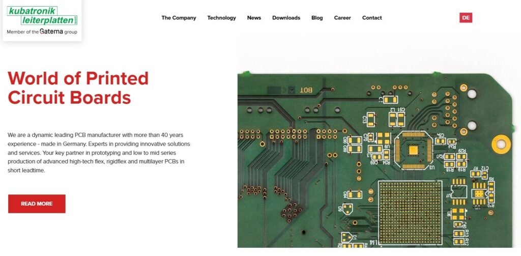
Company Profile
- Year Established: 1980
- Headquarters: Geislingen an der Steige, Germany
- Website: Kubatronik Leiterplatten GmbH
- Headquarter Phone: +49 (0) 7331 96914 39
Key Products
- Multilayer PCBs: Advanced multilayer printed circuit boards for complex electronic applications.
- Flex and Rigid-Flex PCBs: High-quality flexible and rigid-flexible circuit boards suitable for various industrial uses.
- High-Density Interconnect (HDI) PCBs: High-density interconnect boards for advanced electronic systems.
- High-Frequency PCBs: Printed circuit boards designed for high-frequency applications.
Services Offered
- Prototyping: Rapid prototyping services for quick development and testing of PCB designs.
- Small and Medium Series Production: Manufacturing of small to medium-sized production runs to meet specific client needs.
- Express Service: In-time express service for urgent project requirements.
- Technical Consulting: Expert advice on feasibility, material selection, and construction methods.
Certifications
- ISO 9001: Certified quality management system ensuring high-quality production standards.
- ISO 9100: Certified quality management system for aviation and aerospace industries.
- UL 94 V0: Certification for flammability standards of plastic materials.
- RoHS Compliance: Adherence to the Restriction of Hazardous Substances directive.
- REACH Compliance: Compliance with the Registration, Evaluation, Authorization, and Restriction of Chemicals regulation.
Market Applications
- Aerospace: Providing reliable PCBs for aerospace applications.
- Military Technology: Supplying PCBs for military devices requiring high precision and reliability.
- Medical Technology: Delivering PCBs for various medical devices and infrastructure.
- Industrial Applications: Manufacturing PCBs for industrial control systems and automation equipment.
Technological Capabilities
★★★★★ – Kubatronik Leiterplatten GmbH employs advanced manufacturing technologies to produce high-quality PCBs, including:
- Special Materials: Utilization of special materials for specific application requirements.
- Sequential Layer Structures (SBU/HDI): Advanced layer structuring techniques for high-density applications.
- Micro-Fine Structures: Production of micro-fine structures for precise electronic applications.
- Embedded Solutions: Integration of embedded components within PCBs for enhanced functionality.
Sustainability Focus
Kubatronik Leiterplatten GmbH is committed to environmental responsibility through:
- Environmental Management: Implementation of practices to reduce consumption and waste of natural resources.
- Sustainable Production Methods: Adoption of production methods aligned with ecological sustainability.
Global Reach
Kubatronik Leiterplatten GmbH serves clients across Germany and internationally, providing high-quality PCBs for various industries.
Manufacturing Sites & Contact Details
Germany
Geislingen an der Steige Facility
| Plant | Specialization | Address | Phone | |
|---|---|---|---|---|
| Geislingen an der Steige Facility | Prototyping, small and medium series production, and complex PCB manufacturing | Karl-Benz-Straße 13, 73312 Geislingen an der Steige, Germany | +49 (0) 7331 96914 39 | vertrieb@kubatronik.de |
hmp HEIDENHAIN-MICROPRINT GmbH
Company Profile
- Year Established: 1991
- Headquarters: Berlin, Germany
- Website: hmp HEIDENHAIN-MICROPRINT GmbH
- Headquarter Phone: +49 30 54705-0
Key Products
- High-Density Interconnect (HDI) PCBs: Advanced PCBs with high wiring density for complex electronic applications.
- Rigid-Flex PCBs: Combination of rigid and flexible circuit boards for versatile applications.
- High-Frequency PCBs: PCBs designed for high-frequency signal transmission.
- Chip-on-Board (CoB) Technology: Integration of bare semiconductor chips onto the PCB for compact designs.
Services Offered
- Prototyping: Rapid prototyping services for new product development.
- Small to Medium Series Production: Manufacturing services tailored for small to medium production runs.
- Technical Consulting: Expert advice on PCB design and manufacturing processes.
- Quality Assurance: Comprehensive testing and quality control to ensure product reliability.
Certifications
- ISO 9001: Certified quality management system ensuring high production standards.
- ISO 14001: Certified environmental management system demonstrating commitment to sustainability.
- RoHS Compliance: Adherence to the Restriction of Hazardous Substances directive.
- REACH Compliance: Compliance with the Registration, Evaluation, Authorization, and Restriction of Chemicals regulation.
Market Applications
- Industrial Electronics: Supplying PCBs for various industrial electronic applications.
- Telecommunications: Providing PCBs for communication devices and infrastructure.
- Medical Technology: Delivering PCBs for medical devices requiring high reliability.
- Automotive: Manufacturing PCBs for automotive electronic systems.
Technological Capabilities
★★★★★ – hmp HEIDENHAIN-MICROPRINT GmbH utilizes state-of-the-art technology to deliver superior PCB solutions, including:
- Advanced HDI Technology: Production of high-density interconnect PCBs for complex applications.
- Rigid-Flex Manufacturing: Expertise in creating rigid-flex PCBs for versatile designs.
- High-Frequency Material Processing: Specialized in handling materials suited for high-frequency applications.
- Chip-on-Board Integration: Capability to integrate bare chips directly onto the PCB for compact assemblies.
Sustainability Focus
hmp HEIDENHAIN-MICROPRINT GmbH is committed to environmental responsibility through:
- ISO 14001 Certification: Implementation of an effective environmental management system.
- Resource Efficiency: Optimizing production processes to minimize waste and energy consumption.
Global Reach
hmp HEIDENHAIN-MICROPRINT GmbH serves clients across Germany and internationally, providing high-quality PCBs for various industries.
Manufacturing Sites & Contact Details
Germany
Berlin Facility
| Plant | Specialization | Address | Phone | |
|---|---|---|---|---|
| Berlin Facility | Prototyping, small to medium series production, and complex PCB manufacturing | Rhinstr. 134, 12681 Berlin, Germany | +49 30 54705-0 | info@hmp-heidenhain.de |
Micro Circuit Technology GmbH
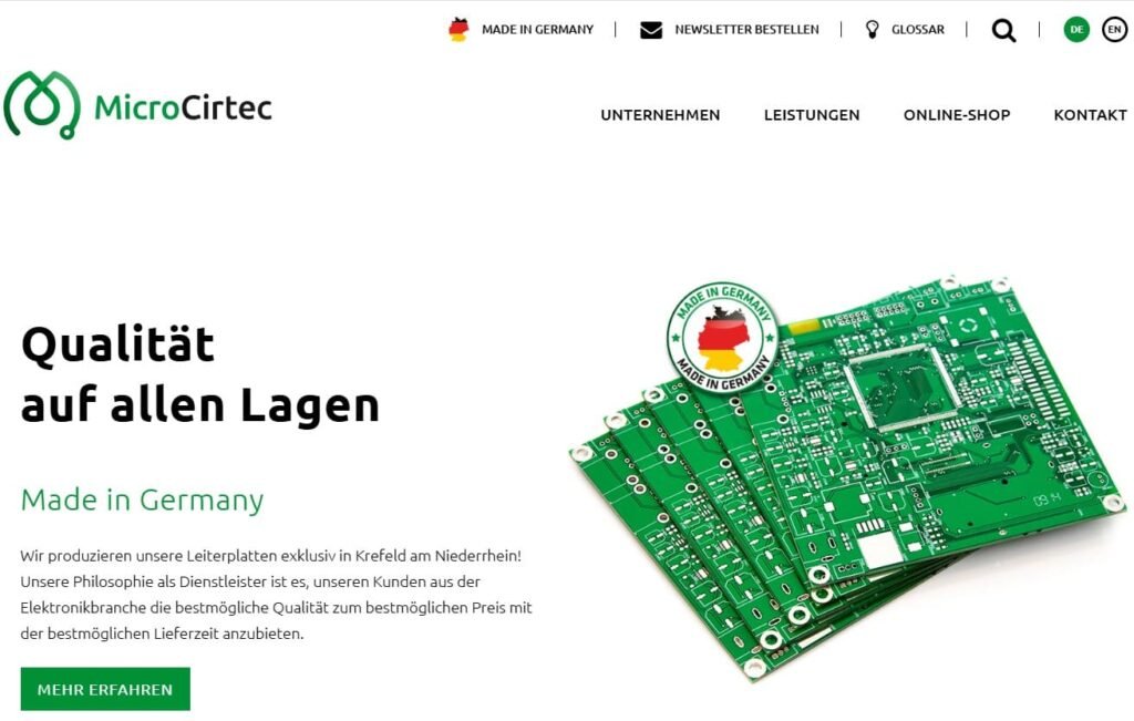
Company Profile
- Year Established: 1984
- Headquarters: Krefeld, Germany
- Website: Micro Circuit Technology GmbH
- Headquarter Phone: +49 (0)2151-825 1
Key Products
- Single and Double-Sided PCBs: High-quality single and double-sided printed circuit boards for various applications.
- Multilayer PCBs: Complex multilayer PCBs with up to 24 layers for advanced electronic systems.
- Semi-Flexible PCBs: Semi-flexible circuit boards designed for specific industrial needs.
Services Offered
- Prototyping: Precision prototyping services to meet specific customer requirements.
- Series Production: Capability to handle both small and large series production runs.
- Express Service: Expedited manufacturing options with delivery times as short as 3 days.
- Online Ordering: Convenient online shop for easy ordering and order tracking.
Certifications
- ISO 9001:2015: Certified quality management system ensuring high production standards.
- RoHS Compliance: Adherence to the Restriction of Hazardous Substances directive.
Market Applications
- Industrial Electronics: Providing PCBs for various industrial electronic applications.
- Renewable Energy: Supplying PCBs for wind energy plants and other renewable energy systems.
- Consumer Electronics: Manufacturing PCBs for a wide range of consumer electronic devices.
Technological Capabilities
★★★★★ – Micro Circuit Technology GmbH employs advanced manufacturing technologies to produce high-quality PCBs, including:
- Automated Production Processes: High technical and automated standards ensure stable quality.
- Quality Control: Consistent production supervision to maintain high-quality standards.
Sustainability Focus
Micro Circuit Technology GmbH is committed to environmental responsibility through:
- Quality and Environmental Management: Focus on quality and the environment in their production processes.
Global Reach
Micro Circuit Technology GmbH serves clients across Germany and internationally, providing high-quality PCBs for various industries.
Manufacturing Sites & Contact Details
Germany
Krefeld Facility
| Plant | Specialization | Address | Phone | |
|---|---|---|---|---|
| Krefeld Facility | Production of single and double-sided PCBs, multilayers, and semi-flexible circuit boards | Oberdießemer Straße 15, 47805 Krefeld, Germany | +49 (0)2151-825 1 | info@microcirtec.de |


