 Skip to content
Struggling to balance your PCB's performance with its manufacturing cost? You’re not alone. Many engineers find it hard to predict the final price, leading to budget overruns and project delays. Understanding the key cost drivers is the first step to taking control.
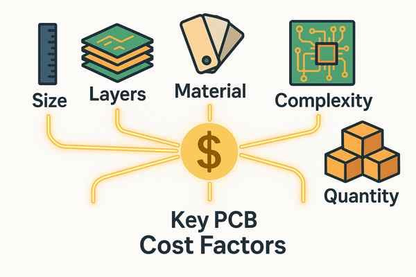
The biggest factors determining your PCB cost are its physical size, the number of copper layers, the material used, the complexity of the manufacturing processes (like trace width and hole size), and your order quantity. Mastering these elements is crucial for cost-effective design.
As a hardware engineer for nearly two decades, I've navigated the trade-offs between cost and technology on countless projects. I’ve seen simple choices made early in the design phase ripple out, causing major budget headaches during production. This article breaks down exactly what you’re paying for—from fundamentals to advanced concepts—and provides actionable strategies to help you design a reliable, cost-effective board.
How Are PCB Costs Calculated?
To effectively manage your budget, you must first understand the bill. Unpredictable quotes make it impossible to plan. Knowing the formula fabricators use to price your board is the key to controlling your final cost.
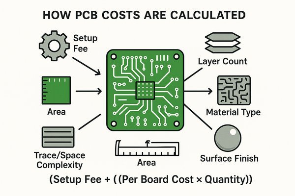
A PCB's cost is calculated by adding a one-time setup fee (tooling) to the per-board manufacturing cost, then multiplying by the quantity. Key factors influencing this include the board's area, layer count, material type, trace/space complexity, and chosen surface finish.
Understanding the Key Cost Components
There isn't a single, universal formula for PCB pricing, but manufacturers follow a "cost-plus" model. The one-time Non-Recurring Engineering (NRE) or tooling cost1 is the initial hurdle. This covers photo-plots, solder mask stencils, and critically, the electrical test fixture. A simple "bed of nails" fixture2 for a low-density board is cheap, but a complex, double-sided fixture with hundreds of test points can increase NRE significantly. Then comes the per-board cost, which is influenced by material usage and processing time. Critically, manufacturers factor in expected yield. If your design has a high aspect ratio (board thickness to smallest drill diameter) exceeding 10:1, they know via plating will be challenging, and yield will drop. If they expect a 90% yield, they will increase the per-board price by about 10% to cover the cost of the inevitable failures. This is why a design that is easy to manufacture is always cheaper.
What Is the Biggest Driver of PCB Cost?
When you need to reduce expenses, where should you focus your effort? Tinkering with minor specs won't make a big impact. To truly slash your PCB cost, you must attack the two factors that drive the price more than any others.
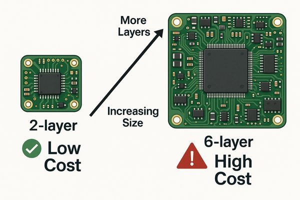
The two biggest drivers of PCB cost are physical size and layer count. A larger board consumes more raw material, and each additional layer adds significant material and processing steps, such as lamination and drilling, which directly increase the final price.
Why Size and Layers Dominate the Cost
While many factors contribute to the final price, board size and layer count have the most substantial impact because they are directly tied to material consumption and machine time. Manufacturers print multiple designs on large standardized panels, often measuring 18x24 inches (457x610 mm), to achieve economies of scale. Physical size dictates how many boards fit on a panel. A 2x2 inch board might fit 108 times, but a 3x3 inch board only fits 45 times. Although the board area only increased by 2.25x, the number of boards per panel was cut by more than half, drastically increasing the per-unit cost. Layer count dictates the complexity of the build. Moving from a 2-layer to a 4-layer board requires an extra core, prepreg, and a full lamination cycle under heat and pressure. It also doubles the number of artwork (photoplot) layers to be imaged and aligned. This jump alone can increase the cost by 35% to 40%. An 8-layer board undergoes this complex lamination and alignment process multiple times, compounding the cost and risk with each step.
How Does the Size of a PCB Affect Its Price?
When trying to lower PCB cost, board size seems like an obvious factor. But the relationship isn't always linear. A tiny increase in dimensions can cause a major price hike, ruining your budget if you don't understand the reason.
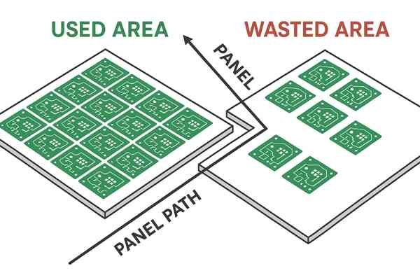
A PCB's price is directly proportional to its surface area because larger boards consume more material. More importantly, the cost is tied to how efficiently your board fits on a standard manufacturing panel. Poor panel utilization means you pay for wasted material.
The Critical Role of Panel Utilization
The core concept to grasp here is panel utilization. Manufacturers use standard panel sizes, such as 18x24 inches, to process boards in large batches. The price you pay is heavily influenced by how many of your boards they can fit onto one of these panels. However, you can't use the entire panel surface. A margin of at least 0.5 to 1 inch is required around the edges for handling and tooling. Furthermore, space is needed between each board for depanelization—typically 0.1" for V-scoring3 and 0.2" or more for tab-routing4. While V-scoring is cheaper, tab-routing is necessary for irregular shapes or designs with edge-hanging components, adding to the cost. Consider an 18x24 inch panel with a 1-inch margin, leaving a usable area of 16x22 inches. If your board is 4x4 inches, you can fit 20 boards (4x5). But if you increase it to 4.2x4.2 inches, you can now only fit 16 boards (4x4). This tiny 5% increase in dimension resulted in a 20% drop in panel efficiency, and your per-unit cost will rise accordingly.
How Does the Number of Layers in a PCB Impact the Cost?
Your routing is complex, and adding layers seems like an easy fix. But this decision has a massive impact on the final PCB cost. If you don't understand why, you risk over-engineering your board and destroying your budget.
Each additional pair of layers increases PCB cost by 20% to 40%. This is because every layer adds material costs (copper foil, prepreg) and requires multiple complex manufacturing steps, including lamination, drilling, plating, and inspection, which extend production time and reduce yield.
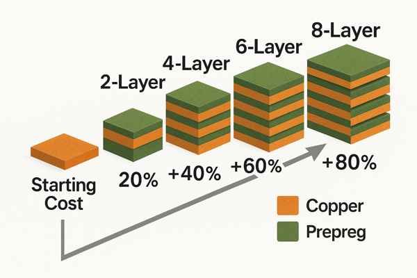
The Lamination Cycle: Adding Cost and Complexity
The cost increase from adding layers is substantial because it introduces entire manufacturing cycles. A lamination cycle is a precise, time-consuming process. To create a 4-layer board, an inner-layer core is first imaged and etched. Then, it's placed in a stack with sheets of prepreg (fiberglass impregnated with uncured resin) and copper foil. This entire stack is placed in a large hydraulic press that applies immense pressure (300-500 PSI) and high temperature (over 350°F or 175°C) for several hours to cure the resin and bond everything together. For high-speed designs, achieving a tight impedance control5 (e.g., ±5%) requires the fabricator to use more expensive, higher-quality prepreg and cores with very consistent thickness, further adding to the cost compared to a standard ±10% tolerance. For an 8-layer board, this sequence of aligning, stacking, and pressing is repeated multiple times. Each step adds a new point of potential failure, directly impacting cost.
| Layer Count Transition | Typical Cost Increase (vs. previous tier) |
|---|---|
| 1-Layer to 2-Layer | ~35% - 40% |
| 2-Layer to 4-Layer | ~35% - 40% |
| 4-Layer to 6-Layer | ~30% - 40% |
| 6-Layer to 8-Layer | ~30% - 35% |
| 8-Layer to 10-Layer | ~20% - 30% |
What Is the Cost Difference Between Various PCB Materials?
Choosing your board material seems simple, but it's a critical cost decision. Sticking with standard FR-4 is cheap, but what if your design needs better performance? You must weigh the significant cost increase of advanced materials.
Standard FR-4 is the most cost-effective material for most applications. High-frequency materials like Rogers or Teflon are significantly more expensive, often costing 5 to 20 times more than FR-4, due to their superior electrical performance and more complex processing requirements.
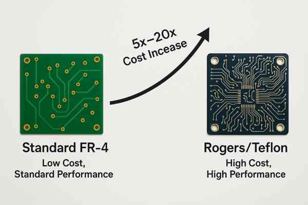
Beyond FR-4: Performance vs. Price
The choice of PCB material directly impacts both performance and cost. For experienced engineers, the key metrics are the dielectric constant6 (Dk), dissipation factor7 (Df), and CAF (Conductive Anodic Filament) resistance8.
| Material Type | Key Characteristics | Best Use Case | Relative Cost |
|---|---|---|---|
| Standard FR-4 | Tg ~140°C. Baseline performance. | General purpose digital & analog < 1GHz | 1x (Base) |
| High-Tg FR-4 | Tg >170°C. Better thermal stability, improved CAF resistance. | Lead-free assembly, automotive, high-power | 1.2x - 1.5x |
| Rogers 4350B | Low Dk (3.66), very low Df (0.0037). Stable over frequency. | RF/Microwave, high-speed digital, antennas | 5x - 10x |
| Hybrid (Rogers+FR-4) | RF material on outer layers, FR-4 on inner layers. | Cost-optimized RF designs | 3x - 6x |
For complex systems, engineers may specify a hybrid stack-up—using Rogers material for the outer RF layers and cheaper FR-4 for the inner power and digital layers. This lowers the cost but adds significant complexity to the lamination process, requiring a fabricator with proven experience with hybrid builds.
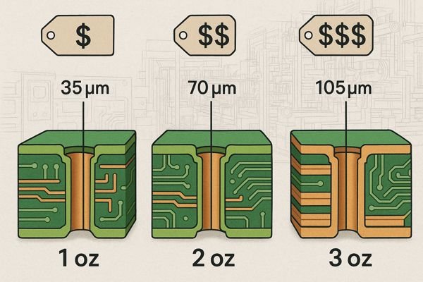
How Does Copper Weight or Thickness Influence PCB Pricing?
For high-current designs, specifying a heavy copper weight seems like a robust solution. But this choice isn't free. This one specification can increase your PCB cost due to material expense and added processing difficulty.
Standard 1 oz copper (1.37 mils or 35 µm thick) is the most cost-effective option. Heavier copper weights (2 oz, 3 oz, or more) increase the price due to higher raw material costs and more difficult, time-consuming etching and plating processes.
The Trade-offs of Heavy Copper
Copper weight has cascading cost implications. Beyond the higher raw material price, heavy copper severely constrains your design rules. During etching, the chemical etchant removes copper vertically but also sideways, a phenomenon known as undercut.
| Copper Weight | Thickness (µm) | Typical Min. Trace/Space | Relative Cost Adder |
|---|---|---|---|
| 0.5 oz | 17.5 µm | 3.5 / 3.5 mil | -5% to 0% |
| 1.0 oz (Std) | 35 µm | 5 / 5 mil | Base |
| 2.0 oz | 70 µm | 8 / 8 mil | +20% to 30% |
| 3.0 oz | 105 µm | 10 / 10 mil | +40% to 60% |
For designs needing localized high-current paths, a more advanced (and expensive) option is selective heavy copper plating, where the fabricator plates up specific traces to 3 oz or more while keeping the rest of the layer at 1 oz. This allows for fine features alongside high-current traces but adds multiple steps to the manufacturing process. For high-power applications, always run a trace width calculation using the charts in the IPC-2152 standard9 to determine the actual copper thickness required, rather than simply over-specifying it.
What Is the Effect of Trace Width and Spacing on the Cost of a PCB?
To shrink your board, you might push for the tightest trace and spacing possible. This common strategy can backfire, dramatically increasing manufacturing costs. Exceeding standard limits moves your board into a premium price tier.
Designs with trace width and spacing of 5 mils (0.127 mm) or greater fall within standard, low-cost manufacturing. Going below this threshold, for example to 3 mils, requires more advanced and expensive processes, potentially increasing the board cost by 25% or more.
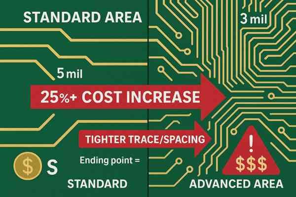
How Tolerances Impact Manufacturing Yield and Cost
The relationship between feature size and cost is directly tied to manufacturing yield. For experienced designers, the conversation moves to features like via-in-pad (VIP)10. While excellent for density and high-speed design, VIPs add significant cost.
| Manufacturing Tier | Min. Trace/Space | Min. Drill Size | Relative Cost |
|---|---|---|---|
| Standard | >= 5 mil | >= 10 mil (0.25mm) | Base |
| Advanced | 3 - 5 mil | 6 - 8 mil (0.15mm) | +25% |
| HDI (Microvias) | < 3 mil | < 6 mil (Laser Drilled) | +100% or more |
A simple VIP that is tented with soldermask is cheap but risky for outgassing during assembly. A VIP that is filled with conductive or non-conductive epoxy and plated flat (VIPPO - Via-in-Pad Plated Over) provides a reliable, solderable surface but adds multiple steps to the process and can increase board cost by 15-25% or more. This is a classic trade-off between density and cost that senior engineers must navigate.
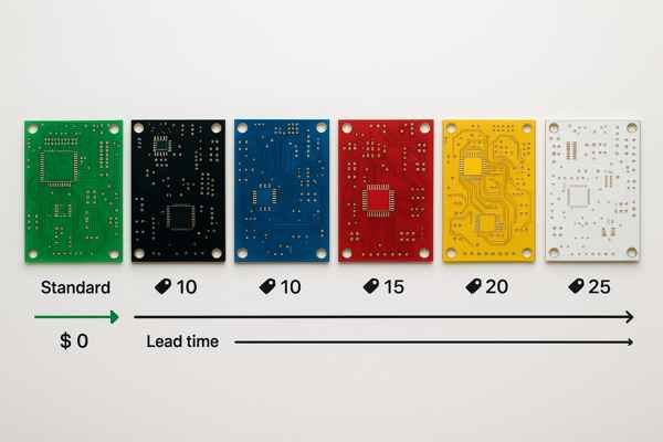
How Much Do Different Soldermask Colors Affect the Price?
Choosing a soldermask color seems like a purely cosmetic decision. But opting for black or blue over standard green can add cost and time to your order. Understanding why helps you decide if the aesthetic is worth the price.
Green is the universal standard for soldermask and is always the cheapest option. Other colors like red, blue, yellow, black, or white often incur a small surcharge, typically $10-$25 for prototype runs, and may require longer lead times due to less frequent use.
The Chemistry and Logistics Behind Soldermask Color
The dominance of green soldermask is deeply rooted in the chemistry of the photolithography process. The diazo-based chemistry used in green LPI has been perfected to achieve the finest feature resolution, allowing for consistent creation of thin soldermask dams between fine-pitch component pads. A subtle but important design choice related to this is the use of solder mask-defined (SMD) vs. non-solder mask-defined (NSMD) pads. For BGAs, NSMD pads are generally preferred as they provide a larger copper surface area for the solder ball to adhere to, improving reliability. However, this requires the soldermask to have a very precise opening. The high resolution of green soldermask makes it ideal for tightly controlled NSMD pads, ensuring better yield and reliability for dense BGA footprints. The pigments in other colors can interfere with this precision, making green the safest technical choice, not just the cheapest.
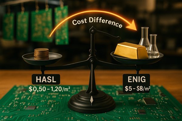
What Is the Cost Difference Between ENIG and HASL Surface Finishes?
The surface finish is a final detail with major cost implications. Are you paying a premium for ENIG when standard HASL would work? Choosing the right finish is a critical balance between your component needs and your budget.
HASL (Hot Air Solder Leveling) is the most economical finish, costing around $0.50 - $1.20 per square meter. ENIG (Electroless Nickel Immersion Gold) is a premium, flat finish that costs 5 to 10 times more, approximately $5 - $8 per square meter, due to the cost of gold and the complex chemical process.
Choosing a Finish: Cost, Reliability, and Performance
The surface finish11 protects the copper from oxidation and provides a solderable surface. For high-reliability applications, the choice goes beyond cost.
| Surface Finish | Planarity | Shelf Life | Key Advantage | Key Disadvantage | Relative Cost |
|---|---|---|---|---|---|
| HASL / LF-HASL | Poor | 12 mo. | Lowest Cost, Robust | Uneven surface, thermal shock | 1x (Base) |
| ENIG | Excellent | >12 mo. | Very flat, good for BGAs, Al wire bonding | Expensive, risk of "black pad" | 5x - 10x |
| Immersion Silver | Excellent | <6 mo. | Very flat, good solderability | Tarnishes, short shelf life | 2x - 3x |
| Immersion Tin | Excellent | <6 mo. | Flat, good for press-fit | Risk of tin whiskers | 2x - 3x |
| Hard Gold | Good | >12 mo. | Extreme durability, wear resistance | Very expensive, poor solderability | 20x - 50x |
Hard Gold (electrolytic nickel and gold) is even more expensive than ENIG but is specified for edge connectors and keypads due to its superior wear resistance. It involves adding cobalt to the gold plating, creating a durable surface that can withstand thousands of insertion cycles.
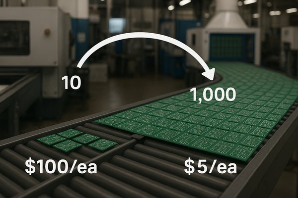
How Does Order Quantity (Volume) Affect the Per-Unit Cost of PCBs?
Your prototype boards are expensive, but the production quote is dramatically lower. This isn't a mistake; it's a fundamental rule of manufacturing. Understanding how volume drives down price is key to planning your production budget.
The per-unit cost of a PCB decreases significantly as order quantity increases. This is because high one-time setup costs (NRE/tooling) are amortized over a larger number of boards. For example, a prototype run of 10 boards may have a high per-unit cost, while a 1,000-unit run is much cheaper per board.
The Math of Mass Production: Amortizing NRE Costs
The relationship between quantity and per-unit cost is driven by the amortization of fixed NRE costs. However, an experienced engineer must also plan for the prototype-to-production transition. A design that works perfectly from a quick-turn prototype shop (optimized for speed) may not be cost-effective at a mass-production facility (optimized for yield and volume). A senior engineer will often design to the mass-production facility's standard rules from the very beginning, even for the initial prototypes, to avoid a costly redesign and re-qualification cycle later. This foresight is a key part of managing total product cost, not just the cost of one batch of boards.
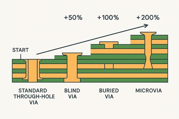
How Do Advanced Features Like Blind, Buried, or Micro Vias Add to the Cost?
To route a dense BGA, you might consider advanced vias. But be warned: these features are not a simple upgrade. Using blind or buried vias introduces immense complexity and is one of the fastest ways to multiply your PCB cost.
Using blind or buried vias can increase PCB cost by 50% to 200% or more compared to a standard through-hole board. This is because they require multiple sequential lamination and drilling cycles, including laser drilling for microvias, which drastically increases process steps and reduces yield.
The Sequential Build-Up Process for HDI Boards
The massive cost of these features comes from sequential lamination. The industry classifies these structures according to standards like IPC-222812.
| HDI Type | Description | Lamination Cycles | Relative Cost |
|---|---|---|---|
| Standard Board | Through-hole vias only | 1 | Base |
| Type I | Blind vias (L1-L2) | 2 | +50% |
| Type II | Blind vias (L1-L2) and buried core vias | 2 | +75% |
| Type III | Stacked/staggered blind vias (e.g., L1-L2, L2-L3) | 3+ | +150% or more |
A complex Type III HDI structure involves multiple lamination cycles for stacked or staggered microvias, with buried vias in the core. For example, an 8-layer board with stacked microvias from L1-L2 and L2-L3 requires at least three separate lamination and plating cycles. Each cycle adds significant time, cost, and risk of failure.
What Are Some Tips for Designing a Low-Cost PCB?
You don't have to sacrifice quality to meet your budget. Designing for cost-efficiency isn't about cutting corners; it's about making smart choices that align with standard, high-yield manufacturing processes from the very beginning.
To design a low-cost PCB, keep the board as small as possible with the fewest layers necessary. Use standard trace/space (>= 5 mil) and drill sizes (>= 0.25mm), stick to a rectangular shape, and choose green soldermask with a HASL finish unless performance dictates otherwise.
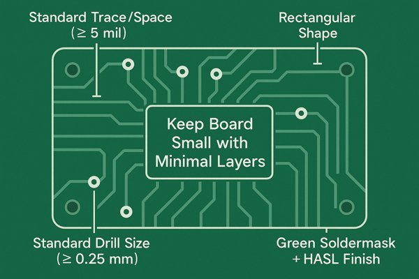
Actionable DFM Strategies for Cost Reduction
As an engineer, I've learned that designing for manufacturability (DFM) is the best way to control costs. Here are my top actionable tips:
- Optimize Size and Shape: Keep your board small and rectangular. Avoid complex shapes or internal cutouts, as these require extra CNC routing time, which adds cost.
- Minimize Layer Count: Before adding layers, exhaust all routing strategies. Can you rotate a component? Can you use a zero-ohm resistor as a jumper? Each layer pair you avoid saves 30-40%.
- Respect Standard Tolerances: Stay comfortably within your fab's standard specs. Aim for 6 mils trace/space and 0.3mm drill sizes. Standardize on a few via sizes to reduce the number of tool changes during drilling.
- Consider Component Selection: The choice between a 0.4mm BGA and a 0.5mm QFP can be the difference between needing an expensive HDI board with microvias and a standard, low-cost 4-layer board. Component selection is a primary driver of board cost.
- Choose Cost-Effective Finishes: Default to Lead-Free HASL. Only pay for ENIG if you have components that demand a perfectly flat surface, like BGAs or press-fit connectors.
- Communicate Early: This is the most important tip. Send your initial stackup and layout to your fab house before you are finished. Their engineers can often provide feedback (e.g., "If you make the board 2mm narrower, you'll get 20% more boards on our panel") that can lead to massive cost savings.
Conclusion
Ultimately, controlling PCB cost comes down to understanding the trade-offs between complexity and price. By focusing on the biggest drivers—size, layer count, and technology choices—you can make informed decisions that keep your project on budget without compromising its essential performance.
-
Understanding NRE costs is crucial for budgeting PCB projects effectively, ensuring you account for all necessary expenses. ↩
-
Learn how 'bed of nails' fixtures are used in PCB testing to ensure quality and reliability, and why their complexity can impact manufacturing costs. ↩
-
Exploring V-scoring will provide insights into cost-effective methods for PCB depanelization and design considerations. ↩
-
Learn how tab-routing affects PCB design, especially for irregular shapes or edge-hanging components, and why it impacts your manufacturing costs. ↩
-
Exploring impedance control will provide insights into its significance in high-speed designs and its impact on overall manufacturing expenses. ↩
-
Understanding dielectric constant helps you choose the right PCB material for signal integrity and high-frequency performance in your designs. ↩
-
Learn how dissipation factor affects signal loss and performance in PCB materials, helping you choose the right substrate for high-frequency designs. ↩
-
Understanding CAF resistance is crucial for selecting PCB materials that ensure reliability and performance in electronic applications. ↩
-
Learn about the IPC-2152 standard to ensure your designs meet high-power application requirements efficiently. ↩
-
Exploring this resource will provide insights into the benefits and challenges of using VIP in PCB design, crucial for optimizing manufacturing. ↩
-
Learn about various PCB surface finishes, their advantages, disadvantages, and how to choose the best one for your project's needs. ↩
-
Exploring IPC-2228 standards will provide insights into industry benchmarks and best practices for HDI board design. ↩


