 Skip to content
Struggling with signal loss in your 5G designs? Your PCB material might be the culprit. Choosing the wrong substrate can cripple performance, especially at high frequencies, leading to costly redesigns.
The best RF PCB materials for 5G applications have a low, stable dielectric constant (\(D_{k}\)) and a very low dissipation factor (\(D_{f}\)). For sub-6 GHz, materials like Rogers RO4350B are excellent. For millimeter-wave (mmWave) frequencies, PTFE-based laminates and advanced ceramic-filled hydrocarbons offer the ultra-low loss performance required.
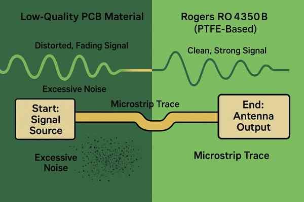
I've spent nearly two decades as a hardware engineer, and I've seen firsthand how a project's success hinges on foundational choices like PCB material. A great design on a poor material will fail, every time. It’s not just about specs on a datasheet; it's about how that material behaves in the real world, under thermal stress, and across production batches. This choice impacts everything from signal integrity to the final product cost. Let's get into the details that matter so you can make the right choice from the start.
How Does Operating Frequency Affect RF Material Selection?
Are your high-frequency signals degrading more than expected? As you push into 5G frequencies, the dielectric properties of your PCB material become a primary performance bottleneck, causing significant signal loss.
For 5G, you must match the material to the frequency band. Below 6 GHz, you can use materials with a dissipation factor (\(D_{f}\)) around 0.004. For mmWave applications (above 24 GHz), you need ultra-low-loss materials with a \(D_{f}\) below 0.002 to maintain acceptable signal integrity.
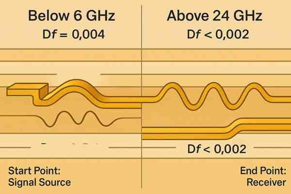
As an engineer, I think about this problem in two distinct categories: the sub-6 GHz band (also known as Frequency Range 1 or FR1) and the millimeter-wave bands (Frequency Range 2 or FR2). The physics of signal propagation changes dramatically between these two realms, and so must our material selection.
Insertion Loss: The Primary Enemy
Insertion loss is the total signal power lost as it travels through the PCB trace. It is a combination of dielectric loss (from the material) and conductor loss (from the copper). As frequency increases, both of these loss components get worse, but dielectric loss becomes especially dominant. This loss is directly related to the material's dissipation factor (\(D_{f}\)). A high \(D_{f}\) means the material absorbs more of the signal's energy and converts it to heat. For example, standard FR-4 has a \(D_{f}\) of around 0.025, which is acceptable at 100 MHz but results in catastrophic loss at 28 GHz.
The Critical Need for Stable Dk and Df
Beyond just being low, the \(D_{k}\) and \(D_{f}\) values must be stable across the entire operating frequency range. Some materials exhibit excellent properties at 1 GHz but degrade significantly at 10 GHz or higher. When I worked on the Tuxedo Keypad at Honeywell, we needed consistent Wi-Fi performance. We had to select a material that maintained a stable dielectric constant1 at 2.4 GHz and 5 GHz to ensure our impedance matching and filter performance didn't drift between bands. Reputable manufacturers like Rogers Corporation provide detailed graphs showing \(D_{k}\) and \(D_{f}\) performance versus frequency, which are essential for making an informed decision.
Material Choices for FR1 vs. FR2
This leads to a clear separation in material strategy.
| Frequency Band | Typical \(D_{f}\) Requirement | Recommended Material Families | Example Materials |
|---|---|---|---|
| FR1 (Sub-6 GHz) | \(< 0.005 \text{ @ 10 GHz}\) | Hydrocarbon Ceramic Laminates | Rogers RO4350B, Isola I-Tera MT40 |
| FR2 (24-40 GHz) | \(< 0.002 \text{ @ 10 GHz}\) | PTFE2, Advanced Ceramic-Filled PTFE | Rogers RT/duroid 5880, Teflon |
| FR2 (\(> 40 \text{ GHz}\)) | \(< 0.0015 \text{ @ 10 GHz}\) | Ultra-Low Loss PTFE, LCP | Rogers RO3003, LCP Laminates |
For a 28 GHz 5G antenna module I helped develop, we couldn't even consider a sub-6 GHz material. We had to use a PTFE-based substrate with a \(D_{f}\) of 0.0017 to meet our link budget. The choice is fundamentally driven by the operating frequency.
How Should An RF PCB Material Be Chosen For High-Power Applications?
Are your power amplifiers overheating and failing? High power generates significant heat, and if your PCB material can't dissipate it effectively, component temperatures will rise, leading to reduced reliability and outright failure.
For high-power RF applications, select a PCB material with high thermal conductivity. A value greater than 0.5 W/m·K is good, and for demanding applications, materials exceeding 1.0 W/m·K are necessary to efficiently transfer heat away from active devices.
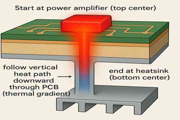
When I'm designing a board with high-power components, like a Gallium Nitride (GaN) power amplifier for a 5G base station, my first thought isn't just about electrical performance. It's about heat. Heat is the enemy of reliability, and your PCB is the first line of defense in getting that heat out.
The Role of Thermal Conductivity (k)
The most critical property for thermal management is thermal conductivity3, symbolized as \(k\) and measured in Watts per meter-Kelvin (W/m·K). This value tells you how efficiently heat can travel through the material. Standard FR-4 is a thermal insulator with a \(k\) value around 0.25 W/m·K. Using it for a high-power device is like wrapping the component in a blanket. Heat gets trapped, the junction temperature skyrockets, and the device eventually fails. High-frequency materials offer a range of thermal conductivities, and choosing the right one is a key design decision.
Balancing Thermal and Electrical Performance
The challenge is that you can't choose a material based on thermal performance alone. You still need excellent RF properties like low \(D_{f}\). A material might have fantastic thermal conductivity but poor loss characteristics, making it unsuitable for the signal path. I once worked on a project where we used a hybrid stack-up. We used a high-thermal-conductivity material directly under the power amplifier and then transitioned to a low-loss material for the RF signal traces. This approach provides the best of both worlds but increases manufacturing complexity.
Advanced Thermal Management Materials
Fortunately, manufacturers have developed materials that excel in both areas.
| Material Type | Example | Thermal Conductivity (\(k\) in W/m·K) | Key Benefit |
|---|---|---|---|
| Hydrocarbon Ceramic | Rogers RO4350B | 0.62 | Good balance of electrical and thermal performance. |
| Thermally Conductive Laminate | Rogers TC350 Plus4 | 1.24 | Excellent for moving heat away from PAs. |
| Ceramic | Alumina (\(Al_{2}O_{3}\)) | 20 - 30 | Superior heat dissipation, but costly and harder to process. |
| Insulated Metal Substrate (IMS) | Aluminum-backed PCB | \(> 1.0\) | Excellent thermal performance, common in power electronics. |
For most 5G power applications, a material like the Rogers TC350 Plus, which Rogers specifically highlights for 5G power amplifiers, is a fantastic choice. It combines a low \(D_{f}\) of 0.0017 with a high thermal conductivity of 1.24 W/m·K, addressing both critical design challenges simultaneously.
How Does The PCB Material Affect Antenna Performance?
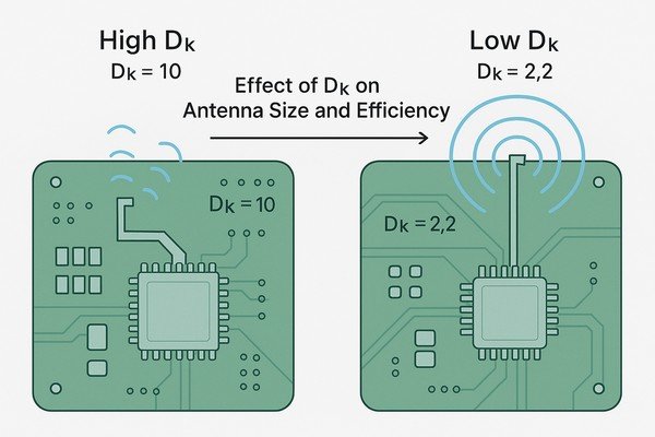
Is your antenna's range and efficiency falling short of simulation? The PCB material itself acts as part of the antenna, and its dielectric constant (\(D_{k}\)) directly influences the antenna's size, bandwidth, and radiation efficiency.
The PCB material's dielectric constant (\(D_{k}\)) is critical for antenna performance. A lower \(D_{k}\) allows for larger antenna elements, which generally improves radiation efficiency and bandwidth. For consistent performance, a material with a stable \(D_{k}\) across frequency is essential.
I've learned this lesson the hard way. Early in my career, I treated the PCB for an antenna as just a mechanical support. The result was an antenna that performed poorly in the real world, despite looking perfect in simulation. The reason was the PCB material.
How Dielectric Constant (Dk) Dictates Size
The antenna's radiating element couples with the ground plane through the dielectric substrate. This means the substrate's properties are an integral part of the antenna's resonant structure. The dielectric constant, \(D_{k}\), directly affects the physical size of the antenna for a given frequency. The length of a common patch antenna is roughly \(\propto 1 / \sqrt{D_{k_{eff}}}\), where \(D_{k_{eff}}\) is the effective dielectric constant. A higher \(D_{k}\) slows the wave, requiring a smaller physical antenna for the same resonant frequency. While this seems good for miniaturization, it comes with penalties.
The Impact on Bandwidth and Efficiency
A smaller antenna on a high-\(D_{k}\) material is often less efficient and has a narrower bandwidth. This is because high-\(D_{k}\) substrates are more prone to exciting and trapping surface waves—energy that travels sideways through the substrate instead of radiating into the air. This trapped energy is lost as heat, reducing the antenna's efficiency. A lower \(D_{k}\) material (closer to air's \(D_{k}\) of \(\approx 1\)) generally allows for a larger, more efficient radiator with wider impedance bandwidth. A material with a \(D_{k}\) of 2.2 might provide 5-8% bandwidth, while a material with a \(D_{k}\) of 10 might only give 1-2%.
The Critical Need for Dk Consistency
For 5G phased arrays, where dozens of small antennas must work together in perfect harmony, consistency is everything. You need a material whose \(D_{k}\) is extremely stable from batch to batch and across temperature and frequency. A small shift in \(D_{k}\) can de-tune the element, altering the phase and ruining the beamforming performance of the entire array. Materials like Rogers' RO4730G3 laminate, with a \(D_{k}\) of 3.0 and a low thermal coefficient of \(D_{k}\) (+26 ppm/°C), are designed specifically for this stability.
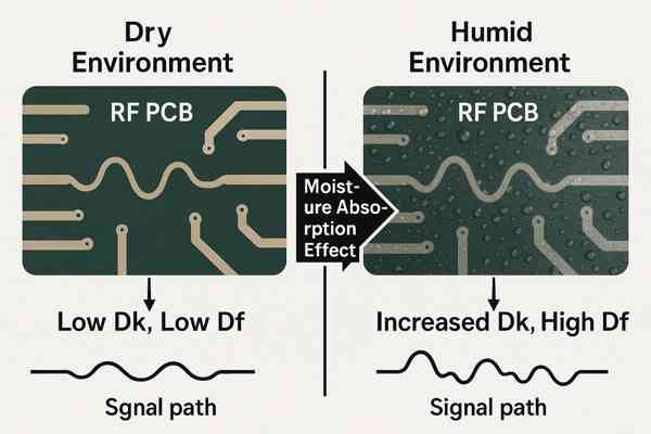
What Is The Impact Of Moisture Absorption On RF PCB Performance?
Does your RF circuit's performance drift in humid environments? Moisture absorbed by the PCB material changes its electrical properties, causing its dielectric constant and loss factor to increase, which detunes filters and reduces signal integrity.
Moisture absorption significantly degrades RF performance by increasing the material's \(D_{k}\) and \(D_{f}\). Materials used in 5G applications should have very low moisture absorption, typically less than 0.1%. Materials like LCP (Liquid Crystal Polymer) and PTFE are excellent choices for this reason.
This is a subtle but critical factor, especially for products deployed globally. I once managed the technical transfer of a product to a manufacturing site in a high-humidity region. We saw performance variations that we couldn't explain until we looked at the material's moisture absorption rate.
Why Moisture is an RF Nightmare
Water has a very high dielectric constant (\(D_{k} \approx 80\)) and is very lossy at RF frequencies. When a PCB substrate absorbs even a tiny amount of water, it's like introducing small, lossy capacitors throughout the material. This has two negative effects: the overall \(D_{k}\) of the material increases, shifting the resonant frequency of filters and antennas, and the overall \(D_{f}\) increases, adding unwanted signal loss. An RF circuit that works perfectly in a dry lab in Arizona might fail completely in a humid environment in Southeast Asia.
Quantifying Moisture Absorption
This property is measured as a percentage of weight gain after a material is exposed to a humid environment, often following the IPC-TM-650 test method 2.6.2.1. A standard FR-4 material can have a moisture absorption rate as high as 0.8%, which is far too high for any serious RF work. The performance would be completely unstable. For high-reliability applications, this is a non-starter.
Selecting Hydrophobic Materials
High-performance materials are engineered to be hydrophobic (they repel water). This ensures their electrical properties remain stable regardless of the operating environment.
| Material Type | Example | Moisture Absorption (\(\%\)) | Stability |
|---|---|---|---|
| Standard FR-4 | N/A | 0.2% - 0.8% | Poor: Unstable \(D_{k}\) and \(D_{f}\). |
| Hydrocarbon Ceramic | Rogers RO4350B | 0.06% | Excellent: Very stable performance. |
| PTFE / Teflon | Rogers RT/duroid 5880 | 0.02% | Outstanding: Extremely low absorption. |
| Liquid Crystal Polymer (LCP) | N/A | \(< 0.04\%\) | Outstanding: Near-hermetic performance. |
For any 5G device, especially those for outdoor use, choosing a material with a moisture absorption rate well below 0.1% is a must. PTFE and LCP are industry leaders in this regard, ensuring long-term reliability.
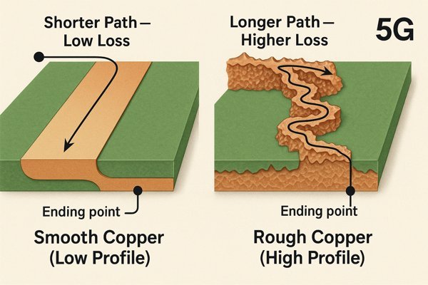
How Does Copper Roughness Affect Signal Loss in RF Circuits?
Have you minimized dielectric loss but still face high insertion loss? The surface roughness of the copper foil on your PCB becomes a major source of conductor loss at high frequencies, effectively making your traces longer and more resistive.
At high frequencies (the skin effect), current flows only on the surface of the copper. A rougher copper surface increases the path length the current must travel, increasing conductor loss. For mmWave 5G, use very smooth (low-profile) copper foils to minimize this loss.
This is a topic often overlooked by designers who focus solely on the dielectric. But at mmWave frequencies, the copper foil is just as important. On a 60 GHz project, we saw 30% more loss than predicted until we traced it back to the copper.
Understanding the Skin Effect
The "skin effect" is a phenomenon where high-frequency AC current concentrates in a very thin layer—or "skin"—on the conductor's surface. The higher the frequency, the thinner the skin. At 1 GHz, the skin depth in copper is about 2.1 µm. By 28 GHz, it shrinks to a mere 0.39 µm. This means the bulk of the copper trace isn't even used by the signal; only the very surface matters.
How Roughness Creates Loss
To ensure good adhesion to the dielectric material, the copper foil is chemically or mechanically roughened. This roughness profile, measured by parameters like \(R_{z}\), can be several micrometers high. If the surface roughness5 is much greater than the skin depth, the current is forced to travel up and down these microscopic hills and valleys. This detour increases the effective path length and the resistive \(I^{2}R\) loss of the trace. It's like taking a winding country road instead of a straight highway—the journey is longer and consumes more energy.
Specifying the Right Copper Foil
This is why specifying the copper type is critical. IPC-4562 details the standards for different foil types.
| Copper Foil Type | Typical Surface Roughness (\(R_{z}\)) | Best for Frequencies | Key Characteristic |
|---|---|---|---|
| Standard ED | 5 - 10 µm | \(< 2 \text{ GHz}\) | High loss, but strong peel strength. |
| Reverse-Treated ED | 3 - 5 µm | \(< 10 \text{ GHz}\) | Smoother side faces the dielectric. |
| Very Low Profile (VLP) ED | \(< 2 \text{ µm}\) | \(> 20 \text{ GHz}\) | Excellent balance of low loss and good adhesion. |
| Rolled-Annealed (RA) | 1 - 2 µm | \(> 10 \text{ GHz}\) | Very smooth, but lower peel strength, better for flex. |
For the 60 GHz project I mentioned, we switched from a standard ED copper with an \(R_{z}\) of ~6 µm to a VLP copper with an \(R_{z}\) under 2 µm. This single change brought our measured performance right back in line with the simulation. For mmWave, specifying VLP copper is not an option—it's a requirement.
Conclusion
Choosing the right RF material is fundamental to 5G success. It involves a careful trade-off between electrical performance, thermal management, and cost, dictated by your specific application and frequency band.
-
Exploring the role of dielectric constant helps in choosing materials that ensure stable performance across frequency ranges. ↩
-
PTFE is known for its low loss characteristics, making it ideal for high-frequency applications like 5G. ↩
-
Understanding thermal conductivity is essential for selecting materials that effectively manage heat in electronic devices, ensuring reliability and performance. ↩
-
Explore the advantages of Rogers TC350 Plus, a top choice for 5G power amplifiers, known for its excellent thermal and electrical performance. ↩
-
Surface roughness plays a vital role in signal integrity. Learn how it impacts conductivity and performance in circuits. ↩


