 Skip to content
Struggling with SMT assembly failures and costly rework? Misplaced components can halt your project, forcing frustrating delays. Properly designed fiducial marks are essential for ensuring a smooth, accurate manufacturing process.
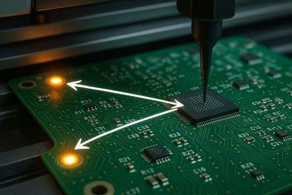
A fiducial mark is a small copper pattern on a printed circuit board (PCB) that a pick-and-place machine's vision system uses as a fixed reference point. This allows the machine to precisely determine the board's orientation and accurately place surface-mount components, especially fine-pitch parts.
Fiducial marks might seem like minor details, but they are one of the most critical elements for successful automated assembly. In my nearly 20 years as a hardware engineer, I've seen projects get delayed simply because these small markers were overlooked or implemented incorrectly. They are the crucial link between your digital CAD design and the physical reality of a perfectly assembled board. Let’s explore why they are so important and how to get them right every time.
Why Are Fiducials Necessary For SMT Assembly?
Your pick-and-place machine is incredibly fast, but it's working blind. Without precise reference points, it can easily misplace tiny components, leading to failed boards and expensive scrap. Fiducials provide the exact alignment needed for repeatable accuracy.
Fiducials are necessary to compensate for mechanical variations in the SMT assembly line. They allow the machine's vision system to detect the exact X-Y and rotational (theta) position of the board, ensuring components like BGAs or 0201 packages are placed with sub-millimeter precision.
Why SMT Machines Need Fiducials for High-Precision Placement
The core issue is a gap in precision. An SMT conveyor system has a mechanical positioning accuracy of around ±0.1 mm. However, modern components require much tighter placement. This "precision gap" is why optical correction is essential.
The table below clearly illustrates how mechanical accuracy falls short for common components.
| Component Example | Required Placement Accuracy | Mechanical System Accuracy | Optical Correction Needed? |
|---|---|---|---|
| 0402 Resistor | < 0.1 mm | ±0.1 mm | Yes |
| 0.5 mm Pitch QFP | < 0.07 mm | ±0.1 mm | Yes, Absolutely |
| 0.4 mm Pitch BGA | < 0.05 mm (50 microns) | ±0.1 mm | Yes, Non-Negotiable |
A fiducial check allows the machine's vision system to build a high-precision coordinate map to correct for offsets, rotation, and even non-linear scaling of the board. It can also instantly detect if a board was loaded incorrectly, preventing the machine from wasting an entire board's worth of components.
What Are The Standard Sizes And Shapes For Fiducial Marks According To IPC Standards?
You've added fiducials to your design, but the assembly house flags a problem. This unexpected feedback forces a last-minute redesign, delaying your prototype schedule. Following industry standards from the start prevents this.
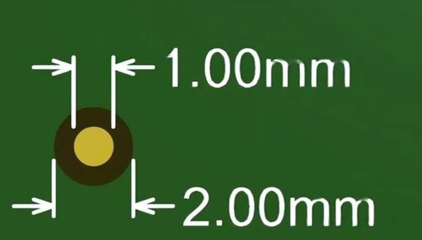
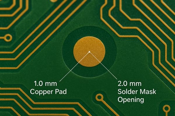
According to the IPC-7351B standard, the optimal fiducial mark is a solid, circular copper pad with a diameter of 1.0 mm. It must have a corresponding solder mask opening that is at least double the pad's diameter, creating a 2.0 mm clearance area.
Key Fiducial Design Rules from the IPC-7351B1 Standard
A solid circle is universally preferred because its center is easy to calculate regardless of rotation. The contrast between the reflective pad and the dark substrate is paramount. For the surface finish2, Electroless Nickel Immersion Gold (ENIG) is ideal due to its superb flatness.
This table summarizes the key IPC-7351B guidelines and the engineering reasons behind them.
| Feature | IPC-7351B Guideline | Engineering Rationale |
|---|---|---|
| Shape | Solid Circle | Symmetrical, non-ambiguous target for vision algorithms. |
| Mark Diameter | 1.0 mm (40 mil) is optimal | Balances visibility with board space. |
| Solder Mask Clearance | Diameter ≥ 2x Mark Diameter | Creates high contrast and prevents solder wicking. |
| Copper Clearance | Equal to Solder Mask Clearance | Prevents nearby copper from confusing pattern recognition. |
| Material Finish | Plated (ENIG preferred) | Ensures a flat, reflective, and non-oxidizing surface. |
Always define the fiducial as a locked component in your ECAD library. This ensures its properties are never accidentally altered and that design rule checks will enforce the necessary clearances.
What Is The Proper Placement For Fiducial Marks On A PCB?
You included fiducials, but the assembly accuracy is still poor on some boards. You're getting inconsistent results, and your assembly partner is struggling. Proper placement is just as critical as the fiducial's design.
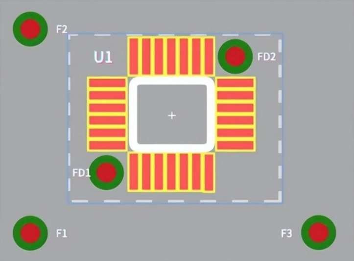
For board-level alignment, place three fiducials in a triangular pattern as far apart as possible, typically near the corners. For fine-pitch components (pitch < 0.5 mm), add two local fiducials diagonally opposite each other within that component's placement area.
Strategic Fiducial Placement for Board-Level and Component-Level Accuracy
A robust placement strategy uses a hierarchy of fiducials. For global fiducials, follow these best practices to avoid common manufacturing issues.
| Guideline | ✅ Do | ❌ Don't | Reason |
|---|---|---|---|
| Quantity | Use three global fiducials. | Use only one or two if avoidable. | Three points resolve all ambiguity (X, Y, rotation, scaling). |
| Pattern | Place in a non-symmetrical triangle. | Place symmetrically or in a line. | Prevents 180-degree rotation errors. |
| Spacing | Maximize distance between them. | Cluster them together. | Increases rotational correction accuracy. |
| Location | Keep >5 mm from the board edge. | Place too close to the edge. | Avoids being obscured by conveyor clamps or rails. |
For local fiducials, place two diagonally on the land pattern of critical components. This provides a final, high-precision correction that accounts for any micro-stretching or twisting of the board in that specific area.
How Much Clearance Is Needed Around Fiducials And Tooling Holes?
Your design gets kicked back from the fab house with a "clearance violation" error. This vague feedback leaves you guessing what rule you broke. Knowing the specific clearance standards for fiducials and tooling holes is key to avoiding DFM holds.
A fiducial needs a solder mask and copper clearance twice its diameter (e.g., a 2 mm zone for a 1 mm fiducial). A standard non-plated tooling hole needs all copper pulled back at least 0.4 mm (16 mils) from its drilled edge.
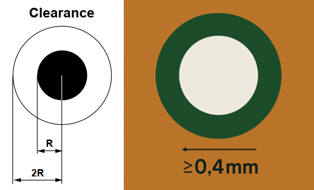
Defining Clearances for Fiducials vs. Tooling Holes3
The clearance rules for fiducials and tooling holes are strict because they prevent two different types of failures. A stray silkscreen designator inside a fiducial's clearance zone is a common error that can blind the vision system. The keep-out zone must be free of everything: other copper, solder mask, and silkscreen.
| Feature | Fiducial Clearance | Tooling Hole Clearance (NPTH) |
|---|---|---|
| Purpose | Optical Integrity | Mechanical Integrity |
| Primary Rule | Solder Mask & Copper Opening ≥ 2x Fiducial Diameter | Copper Pullback ≥ 0.4 mm from edge |
| Keep-out Area | No other copper, mask, or silkscreen in clearance zone | No copper near hole edge; no components near hole |
When Are Both Tooling Holes And Fiducials Required For A PCB Design?
You used fiducials for optical alignment, but your board was unstable on the conveyor. This movement caused inconsistent assembly and damaged some boards. This happens when you don't use tooling holes alongside your fiducials.
Both tooling holes and fiducials are required in virtually all automated SMT manufacturing processes. Tooling holes provide the rough mechanical positioning and stability, while fiducials provide the fine optical alignment. They perform two separate but equally critical functions.
How Fiducials and Tooling Holes Are Used Throughout the SMT Line
Tooling holes and fiducials are used together to ensure consistency as the board moves from one machine to the next. Each process step relies on them for a precise hand-off.
| Production Stage | Primary Mechanical Alignment | Fine Optical Alignment | Purpose |
|---|---|---|---|
| Solder Paste Printing | Tooling Holes | Global/Board Fiducials | Aligns stencil apertures to pads. |
| Pick-and-Place | Tooling Holes | Global, Board, & Component Fiducials | Places components onto paste deposits. |
| Automated Optical Inspection (AOI)4 | Tooling Holes (initial) | Global/Board Fiducials | Establishes a reference grid for inspection. |
| In-Circuit Test (ICT)5 | Tooling Holes | N/A | Aligns test probes in a high-pressure fixture. |
How Do Panel Fiducials Differ From Local Fiducials?
Your panelized boards show a high failure rate, but only on the PCBs in one corner of the panel. This frustrating issue forces you to scrap entire panels. The solution lies in using a multi-level fiducial strategy.
Panel fiducials are placed on the breakaway rails of a panel and are used to align the entire array of boards. Local (or board) fiducials are placed on each individual PCB within that panel to correct for its specific position.
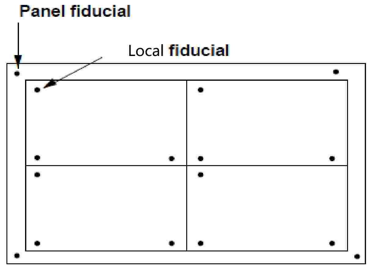
A Multi-Level Fiducial Strategy for PCB Panels
For efficient mass production, a robust fiducial strategy for panels is non-negotiable. This hierarchy ensures accuracy at every level of assembly and can even be used to improve efficiency by identifying bad boards before components are placed.
| Fiducial Type | Location | Primary Purpose |
|---|---|---|
| Panel Fiducial | On the panel's breakaway rails (tooling strips). | Aligns the entire multi-board panel in the machine. |
| Board Fiducial | On the individual PCB itself. | Corrects for that specific board's position within the panel. |
| Component Fiducial | On the footprint of a fine-pitch component. | Provides hyper-local correction for a single critical part. |
| "Bad Mark" Fiducial | On a known-bad PCB within a panel. | Instructs the machine to skip populating that specific unit. |
The "Bad Mark" is an advanced technique where a unique fiducial (e.g., a square) is placed on a unit that failed electrical testing post-fabrication. This tells the assembly line to ignore that board, saving expensive components and time.
Can A Tooling Hole Also Function As A Fiducial?
To save a few square millimeters of board space, you consider using a plated tooling hole as a fiducial. You wonder if this is a clever optimization or a recipe for disaster. It's a question I hear often.
No, a tooling hole absolutely cannot and should not be used as a fiducial. A fiducial needs a flat, highly reflective copper surface for optical recognition. A hole is a void with rough edges and inconsistent lighting, making it an unreliable target for a vision system.
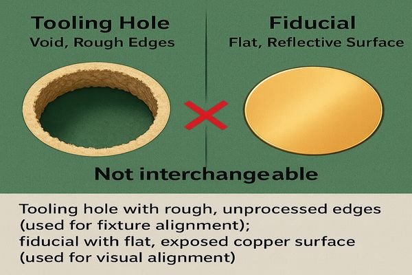
Why a Tooling Hole Fails as an Optical Target
Thinking about this from a signal processing perspective makes the answer clear. A machine vision system is looking for a target with a high signal-to-noise ratio (SNR)6.
- A Proper Fiducial (High SNR): Provides a clean, powerful "signal" (the bright, flat, reflective pad) against a low-"noise" background (the dark, non-reflective solder mask).
- A Tooling Hole (Low SNR): Provides a weak, noisy "signal." The inside of the hole is dark, the drilled edge is rough, and its appearance is highly dependent on unpredictable shadows. It is effectively all noise, with no reliable signal for the system to lock onto.
Attempting to use a tooling hole as a fiducial would dramatically increase the risk of mis-recognition, leading to machine stoppages and assembly defects.
Conclusion
Fiducial marks are not optional decorations. They are a critical design-for-manufacturing element that ensures your boards can be assembled accurately and reliably, saving you time, money, and frustration.
-
Learn about the IPC-7351B standard to ensure your PCB designs meet industry best practices for component footprints and fiducial marks. ↩
-
Learn the different types of PCB surface finishes and their key properties. ↩
-
Learn how tooling holes ensure mechanical alignment and stability during PCB manufacturing, which is crucial for reliable assembly. ↩
-
Learn how AOI ensures quality and accuracy in PCB assembly by detecting defects early in the production process. ↩
-
Learn how In-Circuit Test (ICT) ensures the quality and reliability of assembled PCBs by detecting faults early in the production process. ↩
-
Understanding SNR is crucial for optimizing machine vision systems, ensuring accurate target recognition and reducing errors. ↩


