 Skip to content
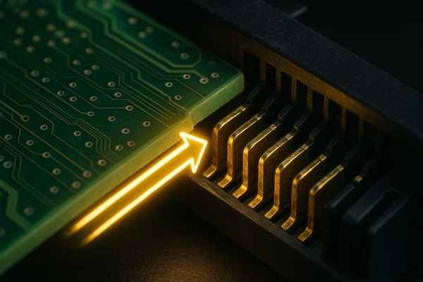
Struggling with unreliable card-edge connections? These failures can cause intermittent system crashes and costly field returns. A robust connection is critical, and that's where gold fingers come in.
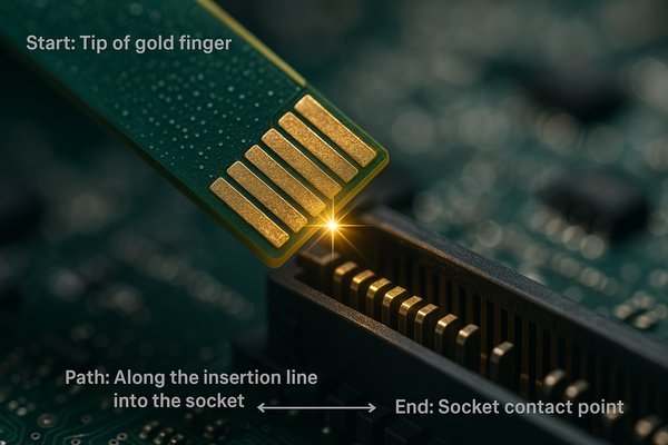
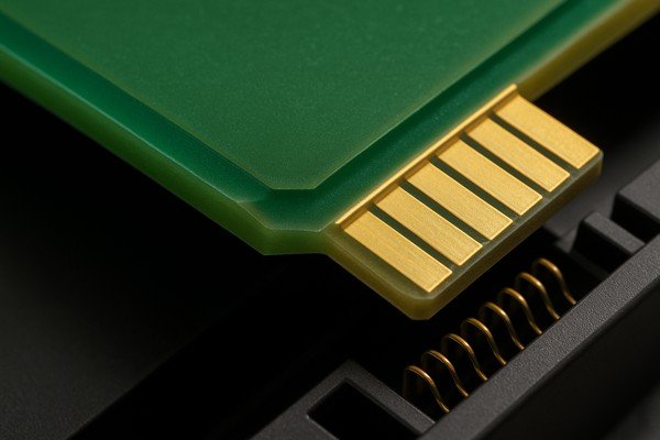
PCB gold fingers are the gold-plated connectors on the edge of a printed circuit board. They are designed for repeated insertions into a socket or slot, providing a durable, corrosion-resistant electrical interface for components like memory modules, graphics cards, and other peripheral devices.
These golden contacts are more than just a surface finish; they are a critical component for any modular electronic system that requires reliability over a long lifespan. In my years of designing everything from industrial controllers to medical devices, I've seen firsthand how a properly specified gold finger design can be the difference between a successful product launch and a debugging nightmare. But to get it right, you need to understand the details—why we use gold, how thick it needs to be, and how to design them correctly in your layout.
What Is the Purpose of Gold Fingers on a PCB?
You need your expansion card to talk to the mainboard. But a bad connection here can cause intermittent faults that are incredibly frustrating to track down, bringing your entire system down.
The main purpose of gold fingers is to create a reliable, wear-resistant, and corrosion-proof electrical connection between a PCB and a socket. They are designed for repeated plugging and unplugging, which is essential for modular systems like computers (RAM, PCIe) and industrial hardware.
The function of gold fingers serves three critical roles that ensure system integrity. I remember a project involving control modules in a high-vibration environment that suffered from random resets. The team spent weeks chasing software bugs, but the root cause was fretting corrosion on a cheap tin-plated edge connector. The micro-vibrations were scraping away the tin oxide, creating conductive dust and intermittent shorts. Switching to a standard 30 µin hard gold finger design completely solved the problem. It was a costly lesson in not cutting corners on the physical interface.
Function 1: Ensuring a Reliable Electrical Connection
Gold is an excellent conductor, ensuring a low-resistance path for signals and power. This is vital for high-speed interfaces where signal integrity1 is paramount. A high-resistance contact, which can be caused by poor materials or corrosion, degrades the signal, shrinks the eye diagram, and ultimately leads to data errors.
Function 2: Providing Mechanical Durability for Repeated Use
These connectors are made to be used. They must withstand the friction of hundreds or even thousands of insertion and removal cycles without wearing out. This is especially critical for hot-swappable enterprise drives or any system where downtime is not an option. This is why we use "hard gold," an alloy specifically designed for this purpose.
Function 3: Offering Environmental Protection from Corrosion
Gold is a noble metal. It doesn't oxidize or corrode when exposed to air and moisture. In a factory or outdoor environment with airborne pollutants, this protection is not a luxury; it's a necessity for long-term reliability.
Why Is Gold Used for PCB Connectors Instead of Other Metals?
Gold is obviously expensive. So why don't we use a cheaper metal like tin or silver for connectors? Using the wrong material is a short-term saving that leads to long-term pain and costly field failures.
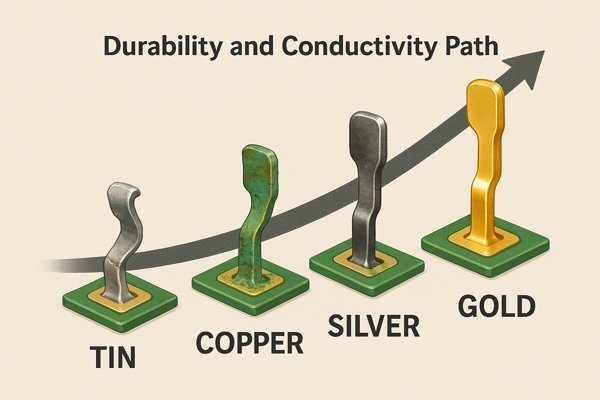
Gold is used because it has the best combination of properties for a reusable connector: high electrical conductivity, outstanding corrosion resistance, and excellent durability when alloyed. Other metals can't compete. Silver tarnishes, copper oxidizes, and tin is too soft to withstand repeated use.
To truly understand why gold is superior, you have to think about the physics of a connection. No surface is perfectly flat; at a microscopic level, it's a series of peaks and valleys called asperities2. When a gold finger meets a spring contact in a socket, the pressure (called normal force) deforms these tiny peaks, creating multiple small, parallel points of contact.
Why Gold's Corrosion Resistance3 Guarantees Reliability
Gold's malleability allows it to deform easily, maximizing the contact area, while its inertness ensures these contact points remain perfectly clean and conductive. Cheaper metals like copper or silver form oxide and sulfide layers that prevent this clean, metal-to-metal contact, leading to higher resistance and connection failures.
The Importance of Hardness for Withstanding Wear
Pure gold is too soft for repeated use. We use "hard gold," an alloy with cobalt or nickel, to withstand the scraping forces of insertion. This hardness ensures the connector survives its intended number of mating cycles without being worn down to the underlying nickel layer.
| Property | Hard Gold (Alloy) | Silver | Tin | Copper |
|---|---|---|---|---|
| Durability (Hardness) | Excellent | Poor | Very Poor | Poor |
| Corrosion Resistance | Excellent | Poor (Tarnishes) | Poor (Oxidizes) | Very Poor (Oxidizes) |
| Suitability for Connectors | Ideal | Not Recommended | Not Recommended | Unusable as surface |
What Are Gold Fingers Made Of?
You can see the gold, but there's more to it than that. If you plate gold directly onto copper, it will fail. The material stack-up is engineered for reliability.
Gold fingers are not solid gold. They are a multi-layer structure. Typically, it consists of a top layer of hard gold (a gold-cobalt alloy) electroplated over a barrier layer of nickel. The nickel itself is plated onto the copper trace of the PCB.
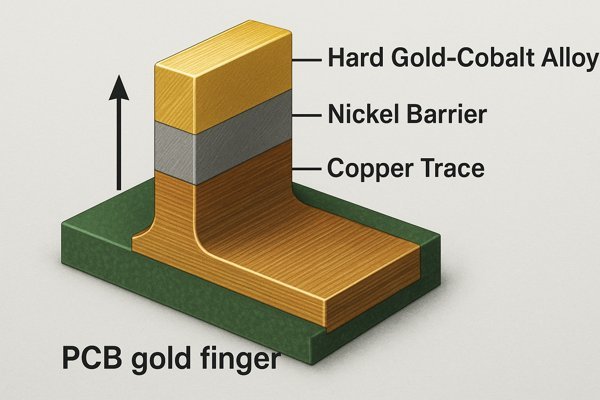
Understanding this layered structure is key to communicating with your PCB fabricator. Each layer has a specific purpose, and if any layer is wrong, the entire connector is compromised. A missing or improperly plated nickel layer is a classic manufacturing defect that leads to rapid failure. The table below summarizes the engineered stack-up.
| Layer | Material | Typical Thickness (µin / µm) | Primary Purpose |
|---|---|---|---|
| Contact Surface | Hard Gold (Gold-Cobalt Alloy) | 15-50 µin / 0.38-1.27 µm | Provides a hard, corrosion-proof, conductive surface for mating. |
| Barrier Layer | Electrolytic Nickel | 100-200 µin / 2.5-5.0 µm | Prevents copper migration into the gold; provides a hard foundation. |
| Conductor | Copper | (Varies by PCB spec) | Forms the electrical trace carrying the signal or power. |
What Is the Difference Between Hard Gold and ENIG?
You've heard of "hard gold" and "ENIG" as PCB finishes. They both use gold, but they are not interchangeable. Choosing the wrong one for your connector will guarantee failure.
Hard gold (electroplated gold) is a thick, durable gold alloy used for mechanical contacts like gold fingers. ENIG (Electroless Nickel Immersion Gold) is a very thin layer of soft, pure gold used for surfaces that will be soldered. ENIG is completely unsuitable for connectors.
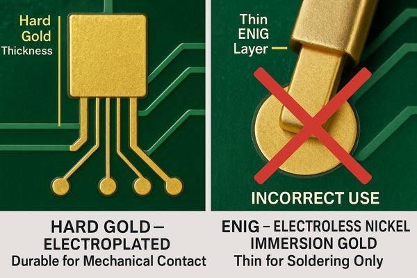
The difference goes down to the manufacturing process. ENIG is an electroless process applied to the entire board before solder mask, covering all exposed copper pads. Hard gold is an electrolytic process applied selectively only to the edge connector. The rest of the board is masked off with tape, and only the fingers are plated. This is why you cannot simply specify "ENIG" for your edge connector; the manufacturing processes are fundamentally different.
| Feature | Hard Gold (Electroplated) | ENIG (Immersion Gold) |
|---|---|---|
| Application | Selective: Applied only to masked areas (edge fingers). | Global: Applied to all exposed copper before solder mask. |
| Process | Electrolytic: Uses an electric current. | Electroless: Chemical deposition process. |
| Gold Type | Gold alloyed with Cobalt/Nickel for hardness. | ~99.9% pure, soft Gold. |
| Gold Thickness | Thick: Typically 30 - 50 µin (0.76 - 1.27 µm). | Thin: Typically 2 - 5 µin (0.05 - 0.12 µm). |
| Primary Use | Wear Surfaces: Edge connectors, keypads. | Solderable Surfaces: BGA pads, QFP pads. |
| Appearance | Bright, shiny, slightly yellowish. | More matte, deeper yellow/orange. |
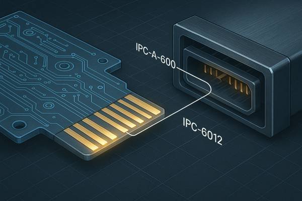
What Are the Industry Standards for PCB Gold Fingers?
Designing in a vacuum is dangerous. If your gold fingers don't meet industry standards, they might not fit into a standard socket, or they might fail prematurely. This can force expensive redesigns.
The primary industry standards governing PCB fabrication and quality are from IPC. Key documents include IPC-A-600 ("Acceptability of Printed Boards") and IPC-6012 ("Qualification and Performance Specification for Rigid Printed Boards"). These define the requirements for materials, thickness, and visual quality of gold fingers.
It's not enough to just know these standards exist; you have to use them effectively. Don't just write "Per IPC standards" on your fabrication drawing. Be specific and reference the performance class you require.
| IPC Class | Description | Typical Application |
|---|---|---|
| Class 1 | General Electronic Products | Consumer electronics, toys where cosmetic imperfections are allowed. |
| Class 2 | Dedicated Service Electronic Products | The industry default. Laptops, servers, industrial controls where long life and reliability are expected. |
| Class 3 | High-Reliability Electronic Products | Medical life support, aerospace, automotive systems where failure is not an option. |
Standard Requirements for Plating Materials and Thickness
The IPC standards specify the Copper -> Nickel -> Gold structure and define performance classes that correlate to plating thickness and quality. For example, they set minimums for the nickel barrier thickness and the final gold thickness depending on the product's reliability class.
Standard Requirements for Dimensional Tolerances
The width of each finger and the spacing between them must be tightly controlled. For a fine-pitch PCIe connector, these tolerances can be as tight as ±0.05mm. Failure to meet this can cause misalignment and intermittent connections.
The Requirement for a Beveled or Chamfered Edge
Nearly all connector standards require a beveled edge on the PCB to prevent damage to the socket during insertion. The angle and depth of this bevel are often strictly defined.
Visual Inspection Criteria Outlined in IPC-A-6004
This standard is the "rulebook" for visual quality. It provides photographic examples of what is acceptable and what is a defect, covering issues like scratches, nodules, contamination, or any sign of the plating peeling off.
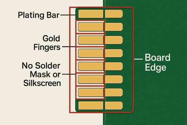
How Do You Design Gold Fingers in a PCB Layout?
Just drawing some pads on the board edge in Altium or Cadence isn't enough. A few common mistakes in the layout phase can cause manufacturing holds or create a faulty board.
In your layout software, place pads on the top and bottom layers at the very edge of the board outline. You must ensure there is no solder mask or silkscreen over the fingers. All fingers must be temporarily connected by a "plating bus" or "plating bar" for the manufacturing process.
Beyond the physical layout, you must consider the electrical performance. For high-speed interfaces like PCIe or USB4, the transition from the PCB trace to the wide gold finger pad is an impedance discontinuity. If not managed, it can cause signal reflections5 that degrade performance.
Step 1: Start with the Mating Connector Datasheet
Always begin with the mechanical drawing for the mating socket. It will give you the exact dimensions: finger width, length, pitch (spacing), and the required board thickness and bevel angle. Never guess these dimensions.
Step 2: Create Pads and Define Keepout Areas
In your EDA tool, create the copper pads for the fingers. Then, draw keepout areas around them to prevent solder mask, copper pours, or silkscreen text from being placed on or too close to the active contact areas.
Step 3: Add a Plating Bus for Manufacturing
For the electrolytic plating process to work, all fingers must be electrically connected. Add a thin trace that connects the very tips of all the fingers together, right at the board edge. This "bus bar" is milled off by the fab house after plating is complete.
Step 4: Address High-Speed Signal Integrity
For high-speed signals, ensure an uninterrupted ground reference plane runs beneath the traces all the way to the fingers. You can also taper the trace width as it approaches the wider finger pad to create a smoother impedance transition.
Step 5: Provide Clear Fabrication Notes
Add explicit notes to your fabrication drawing. Specify the gold and nickel thickness, the bevel angle and depth, and the required IPC class. This removes all ambiguity for your supplier.
What Is a PCB Bevel or Chamfer and Why Is It Used With Gold Fingers?
Trying to jam a sharp, square-edged PCB into a tight, expensive connector is a recipe for disaster. This often-overlooked detail, the bevel, is what separates a professional design from an amateur one.
A bevel, or chamfer, is an angled edge applied to the PCB connector during manufacturing. It is absolutely essential for gold fingers because it creates a smooth, tapered ramp. This allows the board to slide into the mating socket without damaging the delicate spring contacts inside.
The specific angle matters and is often defined by the connector's mechanical standard. Following these specifications is not optional if you want your product to be interoperable and reliable.
| Bevel Angle | Associated Standard / Use Case | Notes |
|---|---|---|
| 20° ±5° | PCI Express (CEM Spec)6 | A shallow angle for smooth insertion into high-density connectors. |
| 30° | Common Industrial / Generic | A good general-purpose angle when no other spec is available. |
| 45° | Older / Less Common Standard | Provides a very aggressive lead-in but can reduce contact surface area. |
Why a Beveled Edge is Critical for Reliability
The ramped edge gently pushes the socket's spring contacts apart. This creates a "wiping action" where the spring contact slides along the gold finger, clearing away any microscopic dust or film and ensuring a clean connection. A sharp 90-degree edge, by contrast, acts like a knife, gouging the contacts and scraping the gold plating.
How to Specify the Bevel in Your Fabrication Notes
You must call this out explicitly in your fabrication drawing. A typical note would be: "Bevel connector edge at 20° ±5°. See detail drawing B." A detail drawing on your fab print is the best way to avoid any misinterpretation by the manufacturer.
How Thick Should the Gold Plating Be on PCB Gold Fingers?
Specifying the gold thickness is a critical trade-off between cost and reliability. Too thin, and your connector wears out prematurely. Too thick, and you are literally plating away your profit margin.
The required gold thickness depends entirely on the number of insertion cycles the product must endure. For standard applications, 30 micro-inches (µin) or 0.76 µm is the most common specification. For high-wear applications, 50 µin (1.27 µm) is necessary.
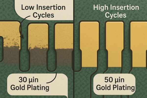
My rule of thumb is based on the cost of failure. If a field failure would cost more than a few hundred dollars to resolve (including technician time, shipping, and customer goodwill), the marginal extra cost for 50 µin of gold is cheap insurance. For a low-cost consumer gadget that might be plugged in once, 15 µin might be acceptable. For a multi-thousand-dollar piece of industrial equipment with a 10-year service life, always specify 50 µin.
| Gold Thickness | Equivalent (µm) | Typical Insertion Cycles | Common Applications & Notes |
|---|---|---|---|
| 3-5 µin | 0.07 - 0.12 µm | < 10 | Not for connectors. This is ENIG (flash gold) for soldering. |
| 15 µin | 0.38 µm | ~250 | Low-cycle consumer electronics. Use only when cost is the primary driver. |
| 30 µin | 0.76 µm | ~1,000 | The industry standard. The best balance of cost and performance for most commercial and industrial products like PCIe cards, RAM modules. |
| 50 µin | 1.27 µm | >2,000 | Heavy-duty use. Test equipment, hot-swappable server components, medical devices, military/aerospace hardware. |
Underneath it all, the nickel barrier layer should be consistently in the range of 100-200 µin (2.5 - 5.0 µm).
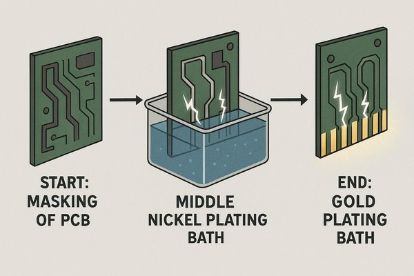
How Are Gold Fingers Manufactured on a PCB?
Ever wondered how a fabricator creates that perfect, shiny gold edge? Understanding the manufacturing process helps you design a board that is easy to build and helps you have more intelligent conversations with your suppliers.
Gold fingers are created using an electrolytic plating process. After the copper traces are etched, all other areas of the board are masked off. The panel is then submerged in chemical baths, first to plate a layer of nickel, and then a layer of hard gold, using an electric current.
The quality of the final product depends heavily on the fabricator's process control. Reputable fabs will use an XRF (X-Ray Fluorescence)7 gun to non-destructively measure the thickness of the nickel and gold layers on test coupons that are processed on the same panel as your boards. You should always ask for this XRF data in your First Article Inspection (FAI) report8.
Step 1: Selective Masking of the Board
A special chemical-resistant tape or a peelable mask is applied to the entire surface of the board panel, leaving only the area of the gold fingers and the plating bus exposed.
Step 2: The Nickel Electroplating Process
The entire panel is submerged in a nickel sulfate bath. An electric current is passed through the plating bus, causing nickel ions to deposit onto the copper fingers and form the hard barrier layer.
Step 3: The Hard Gold Electroplating Process
The panel is then moved to a hard gold plating bath containing gold salts and a hardening agent like cobalt. The process is repeated to deposit the final gold layer to the specified thickness.
Step 4: Final Routing and Beveling
The protective mask is stripped off, other finishes are applied, and then the board is routed from the panel. This routing cut removes the plating bus, electrically isolating each finger. The bevel is then machined onto the edge as the final step.
How Do You Clean Oxidized or Dirty Gold Fingers?
Your system is acting up with random glitches, and you suspect a bad connection. Before you give up on the board, a quick and careful cleaning of the gold fingers could solve the problem.
To clean gold fingers, first blow away loose dust with compressed air. Then, gently wipe the contacts with a lint-free swab or cloth dampened with 99% or higher isopropyl alcohol (IPA). For stubborn grime, you can carefully use a soft, pink pencil eraser.
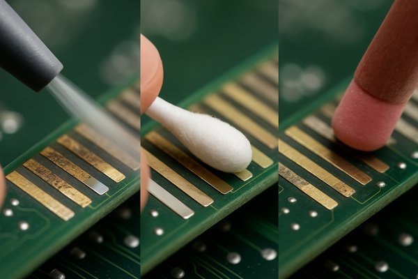
Remember, a connection has two sides. If you clean the gold fingers on your card but the spring contacts inside the mating socket are still dirty, you may not solve the problem. Use the table below as a guide for safe and effective cleaning.
| Tool / Chemical | Recommended Use | ⚠️ Important Cautions |
|---|---|---|
| Compressed Air | First step to remove loose dust and debris. | Hold can upright to avoid discharging propellant liquid onto the board. |
| 99%+ Isopropyl Alcohol (IPA)9 | Removing oils, flux residue, and light films. | Use with lint-free swabs or cloths. Lower purity IPA can leave residue. |
| Contact Cleaner (e.g., DeoxIT)10 | Removing stubborn films and light oxidation. | Ensure it is "plastic-safe." Always follow with an IPA wipe. |
| Vinyl Pencil Eraser | Last resort for physically removing tough grime. | Use very gently. This is an abrasive method that removes a tiny amount of gold. |
| Abrasives (Sandpaper, etc.) | NEVER USE | Will instantly destroy the gold plating and render the card useless. |
| Harsh Solvents (Acetone) | NEVER USE | Can damage the PCB substrate, solder mask, and component markings. |
What Are Common Causes of Gold Finger Failure?
Your card-edge connector has failed. Was it a design flaw, a manufacturing defect, or simply old age? Understanding the root cause is the only way to prevent the failure from happening again.
The most common failures are mechanical wear from too many insertion cycles, corrosion from a porous or scratched plating layer that exposes the nickel underneath, and contamination from oils and dust that create a resistive film on the contact surface.
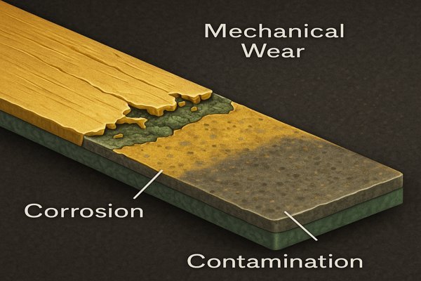
When a product comes back from the field, failure analysis is key. We often use a microscope, and sometimes even a scanning electron microscope (SEM)11, to identify the failure mode. This may seem like overkill, but for a high-volume product, finding the true root cause can save millions.
| Failure Category | Specific Cause | Likely Origin |
|---|---|---|
| Mechanical | Abrasive Wear / Scratches | Normal Use / Misuse |
| Chemical | Porosity Corrosion / Fretting | Manufacturing / Environment |
| Adhesion | Plating Peels or Flakes | Manufacturing Defect |
| Design Flaw | Incorrect Thickness / Missing Bevel | Design Error |
| Contamination | Dust, Oils, Flux Residue | Assembly / Environment |
Are There Any Alternatives to Using Gold Fingers for Edge Connectors?
Gold works great, but it's expensive. In very cost-sensitive designs, engineers often ask if there are cheaper alternatives for card-edge connectors. The answer is yes, but they all come with significant reliability trade-offs.
Yes, there are alternatives, but none match the durability and reliability of hard gold. Cheaper finishes like immersion tin or immersion silver are not suitable for more than a few insertion cycles. A better alternative is often a dedicated two-piece connector system.
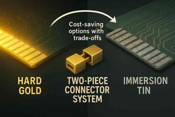
The decision to move away from a card-edge connector is a significant architectural choice. You're trading the simplicity and low cost of a card edge for the higher reliability and performance of a dedicated connector, but at the cost of an additional component on your BOM and another assembly step.
| Connection Type | Relative Cost | Durability (Cycles) | Key Advantage |
|---|---|---|---|
| Hard Gold Card Edge | Medium | 1,000+ | Simplicity and reliability; no extra BOM component. |
| Immersion Tin/Silver | Low | < 25 | Cost only. Not recommended for reusable connections. |
| Two-Piece Connector | High | 500 - 5,000+ | Highest reliability, latching options, high density. |
| ENEPIG Card Edge | Medium-High | ~100 | Better than ENIG, but not a true hard gold substitute. |
This choice isn't just about cost; it's about designing for the entire product lifecycle and the environment it will live in.
Conclusion
Gold fingers are the industry standard for reliable, modular PCB interconnects for good reason. Their engineered hard-gold-over-nickel structure is essential for durability, and proper design following industry standards is not negotiable.
-
Learn how signal integrity impacts data reliability and performance in high-speed electronics, and why it's crucial for preventing errors in your designs. ↩
-
Understanding asperities is crucial for grasping how contact points affect electrical connections. ↩
-
Learn how corrosion resistance impacts the reliability and longevity of electrical connectors, ensuring optimal performance in demanding environments. ↩
-
Explore this link to understand the visual quality standards for PCBs, including real-world examples of acceptable and defective boards as defined by IPC-A-600. ↩
-
Exploring the impact of signal reflections can help you mitigate issues and enhance your PCB's performance. ↩
-
Learn the official PCI Express (CEM Spec) standards for connector bevel angles to ensure your designs meet industry requirements and maximize compatibility. ↩
-
Understanding XRF technology can enhance your knowledge of quality control in manufacturing processes. ↩
-
Exploring FAI reports will help you grasp their significance in ensuring product quality and compliance. ↩
-
Explore this link to learn effective techniques for using IPA safely and efficiently in electronic cleaning. ↩
-
Discover how Contact Cleaner can effectively remove stubborn grime and oxidation from your electronics. ↩
-
Exploring SEM applications can enhance your knowledge of advanced analysis techniques in various fields. ↩


