 Skip to content
Your PCB design looks great, but hidden issues might be lurking. These problems can cause frustrating failures and costly redesigns. Understanding common pitfalls is the first step to avoiding them.
The most common PCB design mistakes often involve poor grounding, incorrect trace widths, neglecting current return paths, and inadequate decoupling capacitors. These oversights can lead to severe signal integrity issues, electromagnetic interference (EMI) problems, and even complete functional failures of your circuit board.

I've spent nearly 20 years in embedded systems and hardware engineering, tackling complex projects from aerospace to medical devices. I've seen my share of designs, both good and bad. One thing I’ve learned is that meticulous attention to detail, especially in the early design stages, can save enormous headaches down the line. Many engineers, especially when under pressure, can overlook some fundamental aspects. Let's dive into some common mistakes and how you, like John, a dedicated Senior Electronics Engineer, can avoid them.
What are the failures of PCB?
PCBs seem robust, but they can fail unexpectedly. This causes major project delays and eats into your budget. Knowing the common failure types helps you design more resilient boards.
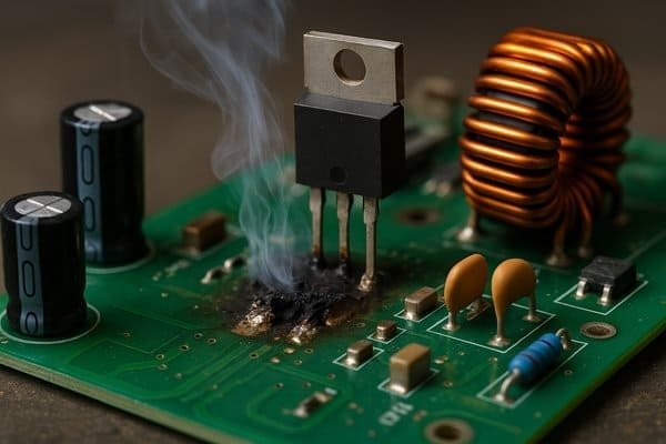
PCB failures broadly fall into electrical (shorts, opens), mechanical (delamination, via cracks), and thermal categories (overheating). These often stem from design oversights, manufacturing defects, or harsh operating environments.
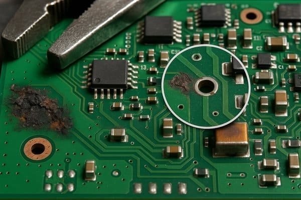
In my experience, especially on high-reliability projects, understanding potential failure modes is critical. A PCB isn't just a piece of fiberglass; it's the backbone of your electronic system. When it fails, everything fails. These failures often don't announce themselves until late in the process, or worse, in the field.
PCB Failure Categories and Causes
| Failure Category | Common Causes | Examples / Impact |
|---|---|---|
| Electrical | Solder bridges, insufficient clearance, open traces | Shorts between signals, loss of signal continuity |
| Incorrect via plating, over-etching | Intermittent connections, complete circuit failure | |
| Mechanical | Thermal stress, vibration, poor material choice | Delamination, cracked vias, broken solder joints |
| Insufficient annular ring, improper handling | Loss of connection through vias, physical board damage | |
| Thermal | Inadequate heat sinking, poor component placement | Component overheating, reduced lifespan, thermal runaway1 |
| Insufficient copper for thermal paths | Performance degradation, premature system failure |
For instance, IPC-2221B2, a generic standard for PCB design, specifies minimum conductor spacing based on voltage levels. For uncoated external conductors at sea level, up to 15V requires 0.13mm (5.1 mils) clearance (B2 classification). Forgetting this can lead to shorts, especially in dense designs. Annular ring requirements, per IPC-A-600 (Class 2 often needs 0.05mm or 2 mils externally), are also vital to prevent via breakout and ensure connection integrity.
What are the golden rules of PCB design?
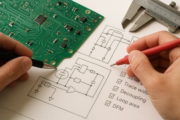
Want truly reliable PCB designs that work the first time? Costly mistakes and endless debugging cycles are frustrating. Following a few golden rules can make all the difference in your projects.
Key golden rules include: ensuring solid grounding and clean return paths, correctly sizing traces for current, using adequate decoupling, minimizing signal loop areas, and always designing for manufacturability (DFM).
Over the years, I've distilled my experience into a set of principles. These aren't just abstract concepts; they are practical guidelines that prevent real-world problems. John, with his high standards, would appreciate these. The most critical, and often overlooked, is the current return path. My central insight is that many subtle EMI and signal integrity issues stem not from the signal trace itself, but from a compromised return path.
Core PCB Design Principles
| Golden Rule | Key Principle | Consequence if Ignored |
|---|---|---|
| Solid Grounding/Return Paths3 | Provide a low-impedance, continuous path for all return currents. | Increased EMI, crosstalk, signal integrity issues, instability. |
| Correct Trace Sizing | Size traces based on current carrying capacity and impedance requirements. | Overheating, voltage drops, signal reflections, impedance mismatch. |
| Adequate Decoupling | Place low-ESR/ESL capacitors close to IC power pins. | Power supply noise, IC malfunction, instability. |
| Minimize Signal Loop Areas | Keep signal and return paths physically close and compact. | Increased EMI radiation and susceptibility. |
| Design for Manufacturability | Adhere to fabricator capabilities and IPC standards. | Manufacturing delays, yield issues, increased cost. |
For high-speed signals (e.g., >50 MHz clocks or rise times < 1ns), controlled impedance (typically 50 ohms single-ended, 90-100 ohms differential) is crucial. This depends on trace width, dielectric height (H), dielectric constant (Er, FR-4 is ~4.0-4.8), and copper thickness. Ignoring this leads to reflections and degraded signals. Always remember, current needs a loop.
What is the 3W rule in PCB design?
Is crosstalk messing with your sensitive signals? This kind of interference leads to unpredictable circuit behavior and can be a nightmare to debug. The 3W rule is a common guideline to help.
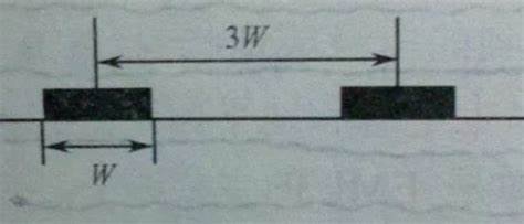
The 3W rule suggests that the centerline-to-centerline spacing between two adjacent critical signal traces should be at least three times the width of an individual trace. This helps minimize electromagnetic coupling (crosstalk).
I've seen many designs where engineers pack traces too tightly to save space, only to battle mysterious noise issues later. The 3W rule is a good starting point for managing this, particularly when routing parallel traces for any significant distance.
Understanding the 3W Rule for Crosstalk Reduction
| Aspect of 3W Rule | Description | Practical Implication |
|---|---|---|
| Definition | Centerline-to-centerline spacing ≥ 3x trace width (W). Edge-to-edge ≥ 2W. | Provides a simple guideline for initial trace separation. |
| Mechanism | Reduces mutual capacitance and mutual inductance between parallel traces. | Lessens the electric and magnetic field coupling that causes crosstalk. |
| Effectiveness Guideline | Can reduce crosstalk by about 70% (approx. -10dB to -15dB voltage coupling). For 10W, can be ~98%. | A good first-pass mitigation, but not a complete solution for severe crosstalk. |
| When to Apply | High-speed signals (clocks, data buses), sensitive analog traces. | Prioritize for signals most likely to be aggressors or victims. |
| Limitations | Effectiveness depends on trace height (H) above reference plane. Not a cure-all. | Closer proximity to a solid reference plane (smaller H) inherently reduces crosstalk more. |
Remember, the 3W rule is a guideline from sources like Howard Johnson's "High-Speed Digital Design." For very critical signals, or when traces are far from their reference plane, more separation or other techniques like guard traces (properly grounded) or orthogonal routing on adjacent layers might be necessary. Always ensure the return path is solid beneath.
What is the 20h rule in PCB?
Are you concerned about electromagnetic interference (EMI) radiating from the edges of your PCB? This can lead to costly compliance failures with standards like FCC or CE. The 20H rule is a technique sometimes suggested to mitigate this.
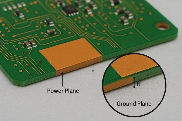
The 20H rule advises that any power plane should be physically smaller than its adjacent ground plane. Specifically, the edge of the power plane should be recessed by at least 20 times the dielectric thickness (H) separating the two planes.
EMI is a constant battle in modern electronics. I've been through many certification processes, and edge radiation can indeed be an issue. The 20H rule aims to tackle one aspect of this by attempting to control fringing fields.
The 20H Rule for Power Plane Edge Management
| Aspect of 20H Rule | Explanation | Key Consideration |
|---|---|---|
| Purpose | Reduce electromagnetic radiation4 from fringing fields at power/ground plane edges. | Aims to improve EMI performance by containing fields. |
| Mechanism (Theory) | Recessing power plane allows ground plane to "capture" fringing fields, reducing radiation. | Based on the idea of managing field coupling at plane boundaries. |
| Calculation | Power plane edge recessed by ≥ 20 * H (dielectric thickness between planes). | If H = 0.2 mm (approx 8 mils), then 20H = 4 mm (approx 160 mils) recession. |
| Implementation | Make power plane polygon smaller than adjacent ground plane polygon in CAD. | Requires careful layer stackup definition and plane shaping. |
| Effectiveness Debate | Debated among EMC experts; often considered marginal compared to other EMC practices5. | Should not be the sole EMI mitigation strategy. Good grounding and decoupling are more critical. |
While the 20H rule is discussed in EMC literature (e.g., by experts like Eric Bogatin), its overall impact is often considered less significant than robust decoupling, continuous ground planes, and minimizing current loop areas. For instance, if your power-ground plane spacing (H) is 0.127 mm (5 mils), the power plane should be pulled back by 20 * 0.127 mm = 2.54 mm (100 mils) from the ground plane edge. It's a practice to consider but not a substitute for fundamental EMC design.
What are the most common PCB design mistakes made in power amplifier driver circuits?
Are your power amplifier or driver circuits oscillating, underperforming, or failing? These circuits are notorious for being tricky, and small layout mistakes can lead to big problems, especially with high currents and fast switching.
Common mistakes in power amplifier driver circuits include poor grounding and layout creating parasitic inductances, inadequate thermal management leading to overheating, insufficient or poorly placed decoupling capacitors causing instability, and incorrect impedance matching of RF signal paths.
I've worked on several projects involving power stages and RF amplifiers, and these circuits demand utmost care in PCB layout. The currents are high (amps), switching speeds can be fast (nanoseconds), and thermal loads are significant (watts).
Avoiding Pitfalls in Power Amplifier/Driver PCB Layout
| Common Mistake Area | Specific Pitfall | Avoidance Strategy |
|---|---|---|
| Grounding & Layout | Large gate drive loop inductance (driver output -> gate -> source -> driver GND). | Keep gate drive loop extremely short and direct. Use wide traces/planes for source return to driver ground. Typically target <5-10nH. |
| Sharing high-current power paths with sensitive control grounds. | Use star grounding for power stages; separate power and control grounds until a single common point. | |
| Thermal Management | Insufficient copper area for heat dissipation from power devices. | Maximize copper planes connected to thermal pads; use multiple layers if needed. Follow device datasheet Rth_jc. |
| Poorly designed or insufficient thermal vias. | Use numerous, large, filled/plated thermal vias directly under thermal pads to conduct heat to other layers. | |
| Decoupling & Stability | Inadequate or poorly placed decoupling capacitors6 for driver ICs/power devices. | Place low-ESR/ESL ceramic capacitors (0.1µF-1µF) very close to Vcc/GND pins. Supplement with bulk capacitance. |
| Parasitic inductance in power supply or ground paths leading to oscillations. | Minimize trace lengths and via counts in power delivery paths to reduce L. | |
| RF Impedance Matching | Mismatched impedance on RF input/output traces. | Use controlled impedance traces (e.g., 50 Ohms) and proper matching networks as per amplifier datasheets. |
A critical point, often my main focus, is the return path for the gate drive current. This high-frequency current must return from the MOSFET/IGBT source to the driver ground via the lowest impedance path, ideally directly under the gate trace on a dedicated ground plane or wide return trace. Any extra inductance here, say 10nH with a 2A/10ns di/dt, can cause a 2V spike (V = L * di/dt), leading to ringing or false triggering.
What is design rule checking in PCB?
Worried that a simple oversight in your layout could render your prototypes unusable or cause manufacturing delays? Manual checking is prone to errors. This is where Design Rule Checking (DRC) becomes essential.
Design Rule Checking (DRC) is an automated process integrated into PCB design software. It systematically verifies whether the physical layout of the board complies with a predefined set of manufacturing constraints and electrical design rules.
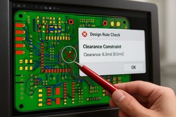
In all my years of designing hardware, from simple boards to complex multi-layer systems, DRC has been an indispensable safety net. It's like having an automated inspector meticulously examining your work before you commit to expensive fabrication. For someone like John, who handles the entire design process, a robust DRC setup is crucial for efficiency and quality.
Key Aspects of Design Rule Checking (DRC)
| DRC Check Category | Example Parameter | Typical Value / Standard (IPC-2221B or mfg.) |
|---|---|---|
| Clearances | Trace-to-Trace, Trace-to-Pad | 0.1 mm - 0.2 mm (4-8 mils) for B2/A2 external (voltage dependent) |
| Copper-to-Board Edge | 0.25 mm - 0.5 mm (10-20 mils) | |
| Trace Attributes | Minimum Trace Width | 0.1 mm - 0.15 mm (4-6 mils) for typical signal traces |
| Acute Angles (Acid Traps) | Generally disallowed or flagged. | |
| Via/Pad Attributes | Minimum Annular Ring (External, Class 2) | Typically ≥ 0.05 mm (2 mils) per IPC-A-600 |
| Minimum Drilled Hole Size | 0.2 mm - 0.3 mm (8-12 mils) for standard capabilities | |
| Plane Checks | Thermal Relief Spoke Width | Sufficient to carry current without starving connection. |
| Plane-to-Drill Clearance | Greater than trace/pad clearances, e.g., 0.25mm (10 mils). |
Setting up DRC correctly involves inputting rules provided by your specific PCB fabricator, as their capabilities define what can be reliably manufactured. For example, a fabricator might specify a minimum trace width of 0.127mm (5 mils) and minimum spacing of 0.127mm (5 mils). If your design violates this, it might be unmanufacturable or have very low yield. Running DRC frequently during layout, not just at the end, catches errors early and saves significant time.
Conclusion
Avoiding common PCB design mistakes, from grounding to DRC, is vital. Understanding return paths and following design rules diligently will ensure your projects are reliable and successful.
-
Understanding thermal runaway is crucial for preventing component failures; this link will explain its causes and how to mitigate risks. ↩
-
This resource will provide you with essential guidelines from IPC-2221B, ensuring your PCB designs meet industry standards and avoid failures. ↩
-
Understanding solid grounding and return paths is essential for preventing EMI and ensuring signal integrity in PCB design. ↩
-
Exploring this topic will provide insights into the challenges and solutions for managing EMI in electronics. ↩
-
Learning about effective EMC practices can significantly improve your electronic design's performance and reliability. ↩
-
Decoupling capacitors play a vital role in stabilizing power supply and reducing noise; learn how to implement them effectively. ↩


