 Skip to content
Your high-speed digital designs are failing, but the logic seems perfect. This frustrating hunt for phantom bugs wastes time and money on board respins. The problem isn't in the code; it's in the copper, and understanding your signaling method is the solution.
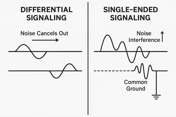
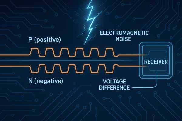
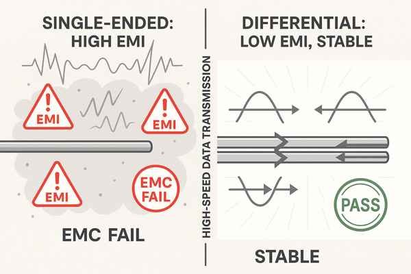
Differential signaling uses two complementary wires to transmit one signal, offering excellent noise immunity, making it ideal for high-speed applications. Single-ended signaling uses one wire referenced to a common ground; it's simpler and cheaper but highly susceptible to noise and ground disturbances.
Choosing the right signaling strategy is one of the most fundamental decisions in hardware design. A single-ended approach might be perfect for a simple LED indicator, but it would be a disaster for a multi-gigabit data link like PCIe or USB. The choice impacts cost, complexity, and most importantly, reliability. In my nearly 20 years as a hardware engineer, I've seen incorrect signaling choices lead to countless hours of debugging, costly board respins, and delayed product launches. Let's break down these two methods so you can make the right choice from the start.
What is differential signaling?
You are tasked with designing a stable high-speed interface like USB or Ethernet. However, random connection drops and data corruption are plaguing your prototypes, threatening your project's timeline and reliability. The robust solution to this high-speed instability is differential signaling.
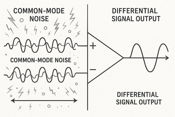
Differential signaling transmits data using a pair of traces, often labeled P (positive) and N (negative). The receiver interprets the voltage difference between these two traces, ignoring noise that affects both lines equally.
A Closer Look at Differential Signaling Standards
Beyond the basic P/N concept, experienced engineers must master different differential standards. While LVDS is common, other standards serve different needs.
| Standard | Typical \(V_{OD}\) | Common-Mode Voltage (\(V_{OS}\)) | Typical Termination | Primary Use Case |
|---|---|---|---|---|
| LVDS | \(350 \text{ mV}\) | \(\approx 1.25 \text{ V}\) | \(100 \text{ }\Omega\) across pair | Board-to-board, backplanes |
| CML | \(400-800 \text{ mV}\) | Varies (often near \(V_{CC}\)) | \(50 \text{ }\Omega\) to \(V_{CC}\) (or termination voltage) | SerDes (PCIe, SATA, XAUI) |
| PECL | \(\approx 800 \text{ mV}\) | \(\approx V_{CC} - 1.3 \text{ V}\) | \(50 \text{ }\Omega\) to \(V_{CC} - 2 \text{ V}\) | High-frequency clocking |
A critical parameter is the receiver's input common-mode voltage range (\(V_{ICM}\)). A receiver can only reject noise if the entire signal (offset + swing + noise) stays within this range. If your \(1.25 \text{ V}\) LVDS signal picks up \(1 \text{ V}\) of common-mode noise, the resulting \(2.25 \text{ V}\) may exceed the receiver's \(V_{ICM}\) limit, causing it to saturate and produce garbage data. This is why AC coupling with capacitors is often used in CML systems—it allows different ICs to establish their own optimal DC common-mode bias without affecting each other.
What is single-ended signaling?
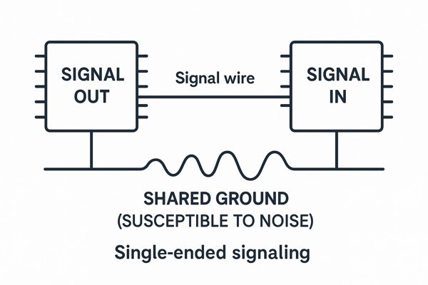
You need a simple and low-cost way to connect components on your board. But be warned, a noisy ground or power rail can easily corrupt these signals, leading to hours of frustrating debugging over seemingly simple connections. To avoid this, you must use single-ended signaling correctly by understanding its limits.
Single-ended signaling uses a single conductor to transmit a signal whose voltage is measured relative to a common ground plane or return path. It's the most common signaling method for general-purpose digital logic.
Real-World Failures of Single-Ended Signaling
While fine for low-speed GPIO, I2C, or SPI, the primary killer of single-ended signaling at scale is Simultaneous Switching Noise (SSN)1, also called ground bounce. The problem can be quantified. A typical BGA package pin might have \(5 \text{ nH}\) of inductance. If a 64-bit data bus switches, and each pin has a current slew rate (\(di/dt\)) of just \(0.2 \text{ A/ns}\), the total ground bounce would be enormous, easily disrupting logic levels. The formula \(V = L \cdot (di/dt)\) shows that even a single pin can be a problem: a fast driver with \(1 \text{ A/ns}\) slew rate through a \(5 \text{ nH}\) inductance creates a \(5 \text{ V}\) spike—a catastrophic event in a 1.8V or 3.3V system.
To combat this, standards for faster single-ended buses evolved. For example, DDR memory interfaces use SSTL (Stub Series Terminated Logic)2. SSTL drivers are designed for a specific termination voltage (\(V_{TT}\)) and use series resistors to control impedance and reduce reflections. It's an enhanced single-ended scheme, but it highlights the extensive effort required to make single-ended work reliably even at moderate speeds.
What is crosstalk in PCB design?
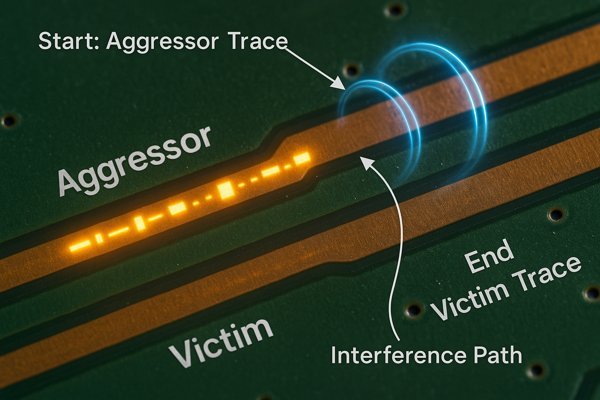
Your board is failing, and you're seeing bizarre, random glitches in your data. You suspect a faulty component, but after hours of desoldering and replacing it, the problem is still there, leaving you completely stumped. The culprit is likely an invisible force called crosstalk, where signals jump between traces.
Crosstalk is the unintentional electromagnetic coupling between adjacent traces on a PCB. A signal switching on one trace, the 'aggressor', can induce a smaller, unwanted signal, or 'noise', onto a nearby trace, the 'victim'.
Practical Crosstalk Analysis: NEXT vs. FEXT
The 3W rule (spacing = 3x trace width) is a common starting point, but it should be treated with extreme skepticism. For high-speed design, using a 2D or 3D field solver to perform a signal integrity simulation is not optional. Engineers must understand the difference between Near-End Crosstalk (NEXT) and Far-End Crosstalk (FEXT)3.
| Crosstalk Type | Measured At | Relationship with Trace Length | Primary Concern For... |
|---|---|---|---|
| NEXT | Driver-end of victim | Largely constant | Short, fast buses |
| FEXT | Receiver-end of victim | Increases with length | Long trace runs |
Worst-case analysis must assume that multiple aggressor nets switch simultaneously, as the total crosstalk is the summation of noise from all nearby aggressors. This is why isolating a critical clock signal from a noisy data bus is a classic layout challenge.
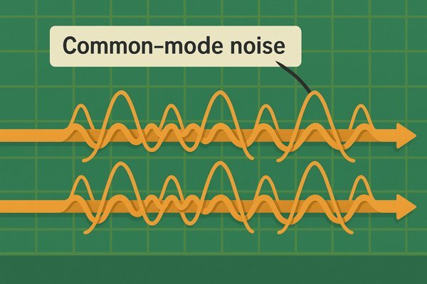
What is common-mode noise?
You’ve perfectly routed your differential pairs with matched lengths and tight coupling. Yet, you're still seeing data errors, making you question if differential signaling even works and leaving you wondering where the noise is coming from. Before you give up, you need to understand common-mode noise.
Common-mode noise is any unwanted voltage that appears with equal amplitude and in the same phase on both conductors of a differential pair. It is noise that is 'common' to both lines relative to ground.
The Engineer's View: How Asymmetry Creates Noise
The Achilles' heel of any differential system is the conversion of common-mode to differential-mode noise, as this converted noise is indistinguishable from the signal. This is caused by asymmetry in the channel.
| Source of Asymmetry | Resulting Effect | Practical Impact |
|---|---|---|
| Length Mismatch | Propagation Time Skew | Converts CM noise to differential jitter |
| Uneven Via Coupling | Impedance Discontinuity | Reflections, mode conversion |
| Fiber Weave Effect | Localized \(D_{k}\) Variation | Velocity skew, deterministic jitter |
| Void in Reference Plane | Return Path Discontinuity | Increased EMI, impedance changes |
The glass fibers in standard FR-4 are not uniform, creating localized areas with a different dielectric constant4 (\(D_{k}\)). This "fiber weave" effect can cause the P and N traces to have slightly different propagation velocities, creating jitter. For 10+ Gbps designs, specifying a specific glass style or rotating the layout 10-20 degrees relative to the fiber weave can be necessary to mitigate this.
Why is differential signaling preferred for high-speed signals?
You are trying to push your data rates into the gigabit-per-second range. At these speeds, your old single-ended signals become noisy antennas, polluting the electromagnetic spectrum, failing EMC tests, and becoming completely unreliable. This is precisely why the industry has moved to differential signaling for all modern high-speed standards.
Differential signaling is preferred for high-speed signals because of its superior immunity to noise, its ability to operate with low voltage swings, and its generation of significantly less electromagnetic interference (EMI).
Under the Hood of High-Speed Performance
The EMI benefit comes from superior return path management. For a tightly coupled differential pair, the return current for the P trace flows primarily on the N trace, and vice versa. This creates an extremely small current loop, resulting in minimal EMI. Furthermore, differential signaling is the foundation for the advanced SerDes equalization5 needed for 5+ Gbps rates.
| SerDes Technique | Location | Function |
|---|---|---|
| Pre-emphasis | Transmitter | Boosts high frequencies to counteract channel loss |
| CTLE6 | Receiver | Provides frequency-dependent gain (equalization) |
| DFE7 | Receiver | Cancels inter-symbol interference from previous bits |
These complex techniques are only practical with the stability and integrity of a differential channel.
What is Common-Mode Rejection Ratio (CMRR)?
You need to select the right differential amplifier for your noisy sensor interface. You're staring at a datasheet full of specifications, unsure which number actually predicts how well the chip will perform against real-world interference. The one spec you must focus on to solve this is the Common-Mode Rejection Ratio (CMRR).
The Common-Mode Rejection Ratio (CMRR) is a metric that quantifies how well a differential receiver rejects common-mode noise. A higher CMRR value, measured in dB, indicates better performance.
Applying CMRR in Real-World Designs
A critical mistake is looking only at the DC value for CMRR. It is highly frequency-dependent, and you must examine the "CMRR vs. Frequency" plot in the datasheet.
| CMRR (dB) | Rejection Factor | Equivalent Differential Noise (from 1V \(V_{cm}\)) |
|---|---|---|
| 40 dB | 100x | 10 mV |
| 60 dB | 1,000x | 1 mV |
| 80 dB | 10,000x | 100 µV |
| 100 dB | 100,000x | 10 µV |
This shows how a 20 dB improvement in CMRR provides a 10x better noise rejection. During the infusion pump design, we had to filter the sensor signal before it reached the amplifier because even with a high CMRR part, the raw noise from nearby medical equipment could have overwhelmed the amplifier's AC rejection capability.
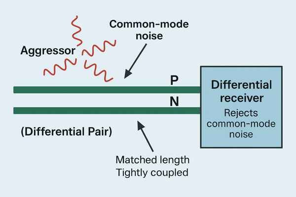
How are differential signals resistant to crosstalk?
You know that differential pairs are supposed to resist crosstalk. But if you just route them carelessly like any other traces, you will completely waste this key advantage and your design may still fail. Their resistance to crosstalk is not automatic; it is earned through a proper layout that understands how they work.
Differential signals resist crosstalk because the noise induced by an aggressor trace couples onto both the P and N lines of the pair as common-mode noise, which is then rejected by the differential receiver.
Key Implementation Details for Layout
To ensure crosstalk couples as common-mode noise, the layout must be geometrically symmetric. Length matching is also more nuanced than just making the final lengths equal. The requirements vary significantly by standard.
| Standard | Data Rate | Max Intra-Pair Skew (Typical) | Equivalent Length in FR-4 |
|---|---|---|---|
| 10/100 Ethernet | 10/100 Mbps | \(\approx 50 \text{ ns}\) | \(\approx 7.5 \text{ m}\) |
| USB 2.0 High-Speed | 480 Mbps | 100 ps | \(\approx 15 \text{ mm}\) |
| PCIe Gen 3 | 8 GT/s | 1.5 ps | \(\approx 0.22 \text{ mm}\) (9 mils) |
| PCIe Gen 4 | 16 GT/s | 0.7 ps | \(\approx 0.1 \text{ mm}\) (4 mils) |
The "serpentine" or "trombone" traces used to add length must themselves be carefully designed. The segments must be long enough and spaced far enough apart (typically >3-5x the trace width) to prevent the fields from coupling and creating an impedance discontinuity, which would harm the signal more than the length mismatch it was intended to fix.
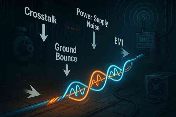
What types of noise does differential signaling reject besides crosstalk?
Your design has to operate in an electrically hostile environment like a factory floor or hospital. The air is filled with interference from motors and power lines that can corrupt your signals, causing system failure at the worst possible time. The solution is a signaling method that can survive this chaos.
Besides crosstalk, differential signaling effectively rejects many other common noise sources, including power supply noise, ground bounce, and radiated electromagnetic interference (EMI) from motors, relays, and radio transmitters.
Engineering Insights from Industrial and Audio Applications
The principle of rejecting common-mode noise is applied across many engineering fields.
| Application | Key Challenge | How Differential Signaling Helps |
|---|---|---|
| Industrial (RS-485) | Large ground potential shifts, motor EMI | Wide \(V_{cm}\) range (\(-7\text{ V to }+12\text{ V}\)) rejects ground offsets |
| Pro Audio (XLR) | 50/60 Hz hum from power lines over long cables | High CMRR input stages reject induced hum |
| Automotive (CAN Bus) | Noise from ignition, injectors, alternators | Twisted-pair cabling provides robust communication |
In each case, the core benefit is the same: the receiver focuses on the difference between the two signal lines, ignoring the common noise that plagues the entire system. This allows for reliable communication whether the goal is high fidelity audio or controlling a critical industrial process.
Conclusion
Single-ended signaling is simple and cost-effective for low-speed, on-board communication. For any high-speed, long-distance, or noise-sensitive application, differential signaling is the only reliable choice due to its outstanding noise immunity.
-
Understanding SSN is crucial for designing reliable digital circuits, as it can significantly impact performance and signal integrity. ↩
-
Exploring SSTL will provide insights into advanced signaling techniques that enhance performance in high-speed digital systems. ↩
-
Learning the distinction between NEXT and FEXT helps engineers design more robust PCBs by addressing specific crosstalk concerns for different trace lengths and configurations. ↩
-
Understanding dielectric constant is crucial for engineers to control signal integrity and minimize noise in high-speed PCB designs. ↩
-
Discover how SerDes equalization enables reliable data rates above 5 Gbps and the role it plays in modern communication systems. ↩
-
Learn how CTLE (Continuous-Time Linear Equalizer) enhances signal integrity in high-speed SerDes systems and why it's crucial for reliable data transfer. ↩
-
Learn how DFE helps cancel inter-symbol interference in high-speed data links, improving signal integrity and enabling faster, more reliable communication. ↩


