 Skip to content
Designing RF PCBs can feel like navigating a minefield. One wrong step in component placement and your circuit's performance can plummet. These errors often lead to frustrating redesigns, project delays, and missed market opportunities. Understanding and applying key placement strategies is your best defense against these costly problems.
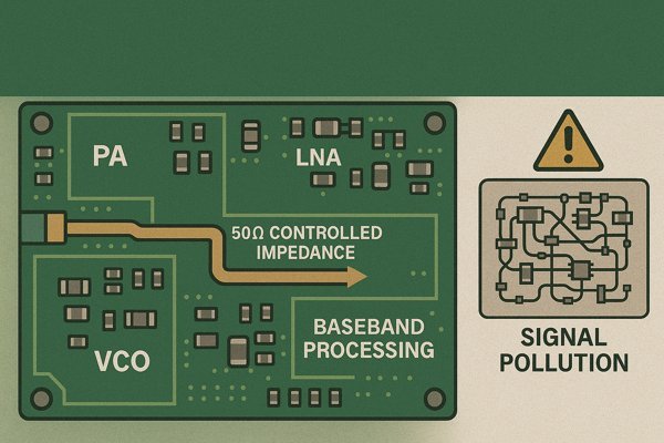
The most critical RF PCB component placement consideration is Functional Bloc Isolation with Controlled Impedance Interconnects. This means you group related components tightly into functional blocks and then strategically place these blocks. This minimizes interference and keeps your signals clean through precisely designed transmission lines.
Getting component placement right is absolutely fundamental for any high-frequency circuit. It’s not just about making things fit; it’s about controlling the electromagnetic fields and ensuring every part of your design works in harmony. I've seen many projects stumble because these principles were overlooked early on. Let's explore the specific details that truly make a difference in achieving a robust and high-performing RF PCB.
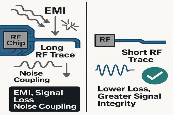
Why is keeping RF signal paths extremely short a primary goal?
Long RF traces on a PCB can act like tiny unintentional antennas. They might pick up noise from other parts of your circuit or radiate energy where you don't want it. This unwanted behavior can seriously degrade your signal quality, cause your device to fail electromagnetic interference (EMI) tests, and ultimately make your product unreliable. The solution is straightforward: keep those RF paths as short as you possibly can.
Keeping RF signal paths extremely short is a primary goal because it minimizes signal loss, reduces parasitic inductance and capacitance, and lessens susceptibility to noise and unwanted radiation. These factors are all crucial for maintaining optimal RF performance and signal integrity.
A Closer Look: The Impact of Path Length on RF Signals
When I talk about keeping RF signal paths short, I'm not just being fussy. There are solid electromagnetic reasons behind this advice.
- Minimizing Signal Loss: At RF frequencies, losses occur due to the skin effect1 and dielectric losses. Shorter paths mean less attenuation. For example, on standard FR-4, losses can be around \(0.1 \text{ dB/cm}\) at 1 GHz, increasing with frequency.
- Reducing Parasitic Inductance and Capacitance: Every trace has parasitic \(L\) and \(C\). A 1 mm wide, 10 mm long, 1 oz copper trace might have roughly \(5 \text{ nH}\) to \(10 \text{ nH}\). Shorter traces reduce these parasitics, which can detune networks.
- Limiting EMI/EMC Problems: Traces longer than \(\lambda/20\) can act as efficient antennas.
- Simplifying Impedance Matching: Shorter paths make it easier to maintain consistent impedance.
Here's a table illustrating how critical trace lengths (where transmission line effects and potential radiation become significant, e.g., \(\lambda/20\)) shrink with increasing frequency:
| Frequency | Wavelength (\(\lambda\)) in Air (approx.) | Critical Length (\(\lambda/20\)) (approx.) | Notes |
|---|---|---|---|
| 100 MHz | \(300 \text{ cm}\) | \(15 \text{ cm}\) | Still relatively long, but good practice matters. |
| 1 GHz | \(30 \text{ cm}\) | \(1.5 \text{ cm}\) | Common for Wi-Fi (lower bands), GPS, Cellular. |
| 2.4 GHz | \(12.5 \text{ cm}\) | \(0.625 \text{ cm}\) (\(6.25 \text{ mm}\)) | Common for Wi-Fi, Bluetooth, Zigbee. |
| 5 GHz | \(6 \text{ cm}\) | \(0.3 \text{ cm}\) (\(3 \text{ mm}\)) | Common for Wi-Fi, other high-speed data. |
| 10 GHz | \(3 \text{ cm}\) | \(0.15 \text{ cm}\) (\(1.5 \text{ mm}\)) | Radar, satellite communication. |
(Note: Wavelength in PCB dielectric will be shorter by a factor of \(1/\sqrt{\epsilon_r}\), where \(\epsilon_r\) is the dielectric constant of the substrate. For FR-4, \(\epsilon_r \approx 4.5\), so \(\sqrt{\epsilon_r} \approx 2.1\). Actual critical lengths on PCB are thus roughly half of the values shown for air).
In my experience, especially on projects like the Tuxedo Keypad at Honeywell where we dealt with Wi-Fi modules, meticulously minimizing trace lengths in the RF front-end was a constant focus. Even a few extra millimeters could impact performance or EMI compliance.
How can RF component orientation affect circuit performance?
It might seem like a minor detail, but just randomly placing and rotating RF components on your PCB can create some unexpected headaches. Incorrect orientation can lead to unwanted coupling between components, which can degrade your signal quality and overall performance. The good news is that a little strategic thinking about how components are oriented can minimize these risks.
RF component orientation can significantly affect circuit performance by influencing parasitic coupling between components, altering current return paths, and impacting the effectiveness of shielding or grounding schemes. These factors can potentially degrade signal integrity and overall system stability.
A Closer Look: Strategic Component Orientation for RF Integrity
The way you orient components, especially those carrying RF signals or susceptible to interference, plays a crucial role in managing electromagnetic interactions on your PCB.
- Managing Parasitic Coupling:
- Inductive Coupling: Minimized by orienting inductors at 90 degrees to each other.
- Capacitive Coupling: Influenced by facing surface areas.
- Controlling Current Return Paths2: Align components for direct ground paths.
- Optimizing Signal Flow and Shielding: Linear flow helps separation.
- Considering Component Asymmetries: Follow datasheet guidelines for directional components.
Here's how inductor orientation can affect mutual inductance:
| Relative Orientation of Two Inductors | Magnetic Field Linkage | Mutual Inductance (\(M\)) | Recommendation for RF |
|---|---|---|---|
| Axes Parallel & Side-by-Side | Maximum | High | Avoid if isolation is needed. |
| Axes Co-linear (End-to-End) | Significant | Moderate to High | Avoid if isolation is needed. |
| Axes Perpendicular (90 degrees) | Minimum | Very Low | Recommended for minimizing coupling. |
| Axes Parallel but Vertically Offset | Reduced | Moderate to Low | Better than side-by-side, but not optimal. |
During the development of a sensitive receiver front-end for a medical device, we found that rotating a particular surface-mount inductor by 90 degrees significantly reduced a spurious signal that was coupling from a nearby digital clock line.
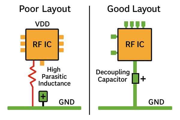
Where is the ideal placement for RF IC decoupling capacitors?
RF Integrated Circuits (ICs) are often the divas of the circuit board – powerful, but incredibly sensitive to any disturbance on their power supply lines. Without proper and meticulously placed decoupling capacitors, your expensive RF IC might decide to oscillate wildly, underperform dramatically, or just give up working altogether. The solution lies in placing these crucial capacitors exactly where they can do the most good.
The ideal placement for RF IC decoupling capacitors is as close as physically possible to the IC's power pins, connected with the shortest and widest traces. This minimizes parasitic inductance in the connection, providing an immediate low-impedance path to shunt high-frequency noise directly at the IC.
A Closer Look: Mastering Decoupling for RF ICs
Decoupling capacitors are essential. Their placement and selection are critical.
- Role: Local energy reservoir and shunting high-frequency noise.
- Minimizing Parasitic Inductance: Short, wide traces to IC pins and ground vias. Even \(1 \text{ nH}\) of inductance has an impedance (\(Z_L = 2 \pi f L\)) of approximately \(6.28 \Omega\) at 1 GHz.
- Using Multiple Capacitor Values: A larger capacitor (e.g., \(1 \text{ µF}\) to \(10 \text{ µF}\)) handles lower frequencies, while smaller ones (e.g., \(100 \text{ nF}\), \(10 \text{ nF}\), \(1 \text{ nF}\), \(100 \text{ pF}\), \(10 \text{ pF}\)) target progressively higher frequencies, placed closest to the pin.
- Connection to Ground: Short, low-inductance path via multiple vias if possible.
- Manufacturer Recommendations: Always consult datasheets for specific values and layout patterns.
Here’s a general guide to selecting decoupling capacitor values for different frequency ranges:
| Capacitor Value Range | Typical Dielectric | Primary Effective Frequency Range | Placement Priority (Relative to IC pin) |
|---|---|---|---|
| \(1 \text{ µF}\) - \(10 \text{ µF}\) | Tantalum, X5R/X7R | \(< 1 \text{ MHz}\) (Bulk Decoupling) | Furthest (among decoupling caps) |
| \(100 \text{ nF}\) (\(0.1 \text{ µF}\)) | X7R, X5R | 1 MHz - 100 MHz | Middle |
| \(10 \text{ nF}\) (\(0.01 \text{ µF}\)) | C0G/NP0, X7R | 50 MHz - 500 MHz | Closer |
| \(1 \text{ nF}\) - \(100 \text{ pF}\) | C0G/NP0 | 100 MHz - few GHz | Closest |
| \(< 100 \text{ pF}\) | C0G/NP0 | \(> 1 \text{ GHz}\) (Very High Frequencies) | Physically touching pin if possible |
(Note: Self-Resonant Frequency (SRF) is key. Above SRF, a capacitor behaves inductively. Smaller case sizes generally have higher SRFs.)
I always tell junior engineers that if an RF IC datasheet shows a specific layout for decoupling, treat it as gospel.
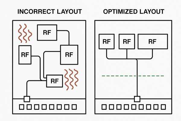
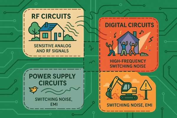
Why physically separate RF, digital, and power supply circuits?
Think of your PCB as a neighborhood. Your sensitive RF circuits are quiet residents. Digital circuits are like a noisy party, and power supply circuits can be like a loud construction site. Interference can corrupt your delicate RF signals. The simplest solution is to create distinct zones for these different circuit types.
Physically separating RF, digital, and power supply circuits is crucial because it minimizes electromagnetic interference (EMI) and crosstalk between these sections. This prevents the high-frequency noise generated by digital logic and power converters from degrading the performance of sensitive analog and RF signals.
A Closer Look: The Art of PCB Partitioning for Signal Integrity
Isolating different types of circuitry is fundamental for managing noise.
- Noise Sources:
- Digital: Fast rise/fall times, broad spectrum of harmonics. A 100 MHz clock can have harmonics into the GHz range.
- Power Supply (SMPS): Switching noise, sharp transients.
- RF: Sensitive to low-level signals (e.g., down to \(-100 \text{ dBm}\)).
- Layout Strategies:
- Zoning: Divide PCB into RF, digital, power regions.
- Ground Plane Management3: Solid ground plane preferred, with careful component placement.
- Trace Routing: Keep digital traces away from RF; cross at 90 degrees if necessary.
- Filtering and Shielding: Use filters on lines crossing zones; consider shielding cans.
- Practical Distances: Millimeters to centimeters, or shielding, depending on noise levels (e.g., if digital signals are \(>100 \text{ MHz}\)) and sensitivity.
Here's a summary of characteristics and separation strategies:
| Circuit Type | Primary Noise Characteristics | Susceptibility | Key Separation / Isolation Strategies |
|---|---|---|---|
| RF / Analog | Low-level signals, sensitive to external noise | Very High | Physical distance from noisy circuits, shielding, dedicated ground/power, filtering at I/O. |
| Digital | High-frequency harmonics from fast switching edges | Low to Moderate (to noise) | Containment of noisy traces, controlled impedance, termination, distance from RF. |
| Power (SMPS) | Switching noise (conducted & radiated), voltage ripple | Can affect all circuits | Input/output filtering, shielding of inductors/switching nodes, physical separation, careful layout of high current loops. |
At Honeywell, for the Tuxedo platform, PCB partitioning was an art form to ensure reliable RF performance alongside the noisy digital core.
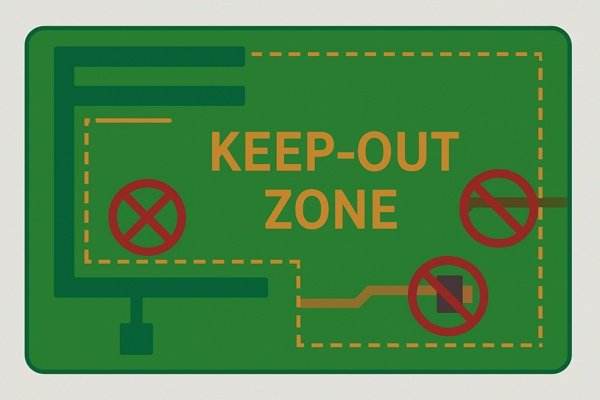
What is a "keep-out zone" near a PCB antenna?
Antennas need personal space. Placing other components, traces, or ground planes too close can severely detune an antenna, reduce efficiency, and mess up its radiation pattern. Defining a "keep-out zone" gives your antenna the breathing room it needs.
A "keep-out zone" near a PCB antenna is a specifically defined area on the PCB around the antenna element where no components, copper traces (especially ground planes on any layer), or metallic objects should be placed. This precaution is vital to prevent unwanted electromagnetic interactions that can detune the antenna and degrade its radiation performance.
A Closer Look: Ensuring Antenna Performance with Keep-Out Zones
The keep-out zone is critical for any PCB-mounted antenna.
- Why Antennas Need Space: Nearby conductors and dielectrics can detune the antenna, alter impedance, and affect the radiation pattern.
- Defining the Keep-Out Zone:
- Manufacturer Datasheets: Primary source for keep-out dimensions (e.g., a 2.4 GHz chip antenna might require 5mm x 5mm or 10mm x 10mm on all layers).
- Ground Plane Clearance: Specific requirements for ground under or near the antenna.
- No Components or Traces: Strictly enforce within the zone.
- Enclosure Considerations: Metallic enclosures are challenging. Keep antennas 5mm to 10mm away from plastic housing if possible.
General guidelines for antenna keep-out zones (always defer to manufacturer specs):
| Antenna Type | Typical Keep-Out Considerations | Ground Plane Interaction | Material Sensitivity |
|---|---|---|---|
| Chip Antenna | All layers around and often below (unless specified otherwise). Sizes vary from a few mm to >10mm. | Often requires specific ground clearance or a defined ground plane area nearby. | Sensitive to dielectrics. |
| Trace Antenna | Area around the trace on all layers. | Designed with specific ground plane shape/size and clearance. | Sensitive to dielectrics. |
| External (SMA/U.FL connected) | Keep-out around the connector footprint and launch trace. | Ensure proper \(50 \Omega\) launch from connector to feed point. | Less PCB sensitivity for antenna element itself. |
I recall a project where a last-minute metal bracket near a Bluetooth antenna violated its keep-out zone, causing communication range to plummet.
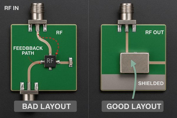
How should RF amplifier input/output stages be positioned?
RF amplifiers can oscillate if their output feeds back into the input. This instability can damage the amplifier or render the RF chain useless. Careful input/output positioning is key to amplifier stability.
RF amplifier input and output stages should be positioned to maximize physical separation and ensure a clear, unidirectional signal flow. Often, this involves placing grounding structures or even physical shielding between them to prevent feedback paths that could lead to instability and oscillation.
A Closer Look: Ensuring Amplifier Stability Through Layout
Physical layout is critical for stable RF amplifier operation.
- Feedback Mechanisms4: Capacitive, inductive, ground loops, power supply coupling.
- Layout Strategies for Isolation:
- Linear Signal Flow: Input -> Matching -> IC -> Matching -> Output.
- Physical Separation: Maximize distance between input/output.
- Grounding: Solid ground plane, "star" ground for IC paddle (multiple vias, e.g., a \(3 \times 3\) or \(4 \times 4\) array with 0.8mm-1.27mm pitch), guard grounding/via stitching (vias spaced \(<\lambda/20\) apart).
- Orthogonal Placement: For nearby input/output inductors if separation is limited.
- Manufacturer Guidelines: Follow datasheet layout examples. Isolation of \(>40 \text{ dB}\) to \(60 \text{ dB}\) might be needed.
Here's a table summarizing common feedback issues and layout solutions for RF amplifiers:
| Feedback Mechanism | Description | Layout Solution(s) |
|---|---|---|
| Capacitive Coupling | Electric field from output traces couples to input traces. | Increase physical separation between input/output traces. Use ground shielding traces or planes between input/output. |
| Inductive Coupling | Magnetic field from output current loops couples to input current loops. | Maximize distance between input/output inductors/loops. Orient inductors perpendicularly. Minimize loop areas. |
| Common Ground Impedance | Input and output currents share a ground path with non-zero impedance. | Use a solid, low-impedance ground plane. Provide separate, direct ground returns for input and output stages to a common point (star ground at IC). |
| Power Supply Coupling | Output stage noise couples to input via shared power supply lines. | Robust decoupling for input and output stages. Separate power supply traces if possible, or use ferrite beads for isolation. |
During LNA bring-up, rerouting a bias line and adding a small ground shield trace solved an oscillation issue.
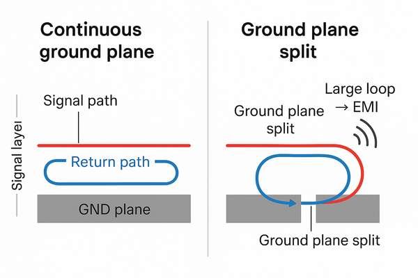
What risk is there in placing RF parts over ground plane splits?
Ground plane splits, intended to isolate sections, can be a trap for RF signals if not handled with extreme care. Placing RF components or traces over a split can severely disrupt the signal's return current path, leading to noise, radiation, and unpredictable behavior.
Placing RF parts or traces over ground plane splits poses a significant risk because it forces RF return currents to take longer, convoluted, and higher-impedance paths. This interruption increases the signal loop area, leading to increased noise susceptibility, common-mode radiation, and unpredictable impedance characteristics for the RF trace.
A Closer Look: The Perils of Ground Plane Splits for RF Circuits
Understanding RF return currents is key.
- RF Return Current Behavior: At high frequencies (e.g., \(> \text{few MHz}\)), return current flows directly under the signal trace to minimize loop inductance.
- Impact of a Split:
- Interrupted return path.
- Increased loop area (EMI emission/susceptibility).
- Increased inductance and impedance discontinuity (reflections).
- Voltage differences across the split (common-mode noise).
- When Splits Are (Cautiously) Used: For isolating very noisy digital from sensitive analog. Signals must cross at a single point with a return path bridge. RF signals should generally never cross a split without a direct bridge.
- Preferred Approach for RF: A solid, continuous ground plane. Isolation via partitioning and careful routing.
Comparison of Grounding Strategies for RF Traces:
| Feature | Solid Ground Plane Under RF Trace | Split Ground Plane Under RF Trace (No Bridge) | Split Ground Plane with Proper Bridge Under Trace |
|---|---|---|---|
| Return Current Path | Direct, low inductance | Indirect, convoluted, high inductance | Direct (follows bridge), low inductance |
| Signal Loop Area | Minimized | Maximized | Minimized at bridge point |
| Impedance Control | Consistent | Disrupted, unpredictable | Maintained if bridge is well-designed |
| EMI/EMC Performance | Good | Poor (high radiation/susceptibility) | Can be good if bridge is localized |
| Recommendation for RF | Highly Recommended | Strongly Discouraged | Use with extreme caution, only if necessary |
I've seen designs where an RF trace unknowingly crossed a small ground gap, causing intermittent instability. Stitching the gap fixed it.
Where should RF filters ideally be located in a signal chain?
Unwanted signals can desensitize receivers or cause transmitters to fail emissions tests. RF filters are your primary weapon, but their location is critical for effectiveness.
RF filters should ideally be located as close as possible to the component they are protecting or whose output they are cleaning. Common strategic locations include directly at an antenna input/output, or immediately before and/or after active components like mixers and amplifiers to suppress unwanted products or out-of-band signals.
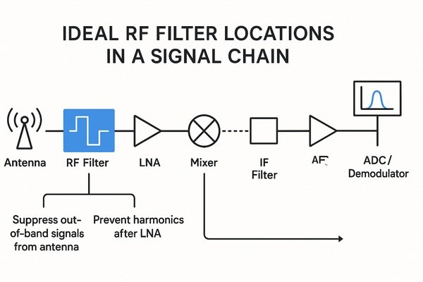
A Closer Look: Strategic Placement of RF Filters
The effectiveness of an RF filter5 is maximized when it's placed to intercept unwanted signals promptly.
-
Key Filter Locations and Their Rationale:
Location Purpose Filter Type Example Why Proximity Matters Antenna Input (Receiver) Suppress out-of-band interference before LNA; protect LNA from overload Band-Pass Filter (BPF) Prevents strong out-of-band signals from saturating the LNA or creating IMD. Antenna Output (Transmitter) Attenuate harmonics and spurious emissions from PA Low-Pass Filter (LPF) Ensures compliance with regulatory emission masks (e.g., FCC, ETSI). Before Mixer (LO Port) Clean up Local Oscillator signal, remove harmonics BPF or LPF Prevents LO harmonics from creating unwanted mixing products. After Mixer (IF Port) Select desired Intermediate Frequency (IF); reject image frequency, LO leakage BPF Crucial for image rejection; image frequency is often \(F_{\text{signal}} \pm 2 \times F_{\text{IF}}\). An image reject filter might need \(>60 \text{ dB}\) rejection. Interstage (Between Amplifiers) Limit bandwidth, improve stability, filter out noise/distortion from previous stage BPF Prevents amplification of out-of-band noise or spurious signals. Before ADC/DAC (SDRs/Digital RF) Anti-aliasing (ADC) or DAC image removal (DAC) LPF (Anti-aliasing), BPF Prevents aliasing in ADCs; removes DAC images and smoothing. -
Impedance Matching6 is Crucial: Filters (LC, SAW, ceramic) need specific source/load impedances (typically \(50 \Omega\)). Mismatch degrades performance.
-
Minimize Trace Lengths To/From Filter: Reduces noise pickup on unfiltered/filtered lines.
-
Grounding and Shielding of Filters: Vital for performance.
At Smiths Medical, the transmitter output LPF was placed directly at the PA output for clean emissions, critical for medical environments.
How does component proximity influence RF thermal issues?
RF power components like PAs generate significant heat. This heat can affect nearby parts, causing performance drift, reduced lifespan, or failure. Smart placement considering thermal paths is crucial.
Component proximity significantly influences RF thermal issues because heat-generating components (like Power Amplifiers or LDOs) can elevate the temperature of nearby thermally sensitive parts (like Voltage-Controlled Oscillators, ADCs, or precision references). This can alter their electrical characteristics, leading to performance degradation or system instability. Proper spacing and thermal management techniques are essential.
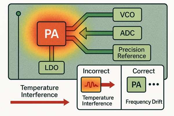
A Closer Look: Managing Heat in RF PCB Layouts
Effective thermal management through component placement is vital.
- Heat Generators: PAs (e.g., a 5W PA, 50% efficient, dissipates 5W heat), LDOs (\(P_{\text{diss}} = (V_{\text{in}} - V_{\text{out}}) \times I_{\text{load}}\)).
- Thermally Sensitive Components: VCOs (frequency drift, e.g., tens of ppm/\(^{\circ}\text{C}\)), ADCs/DACs, LNAs (noise figure), XOs (drift 20-100 ppm).
- Thermal Coupling: Conduction (PCB copper), Convection (air), Radiation (infrared).
- Placement Strategies:
- Isolate hot from sensitive.
- Heatsinking with copper pours and thermal vias (IPC-2152 for guidance).
- Thermal vias7: arrays under pads (e.g., 0.3mm-0.5mm diameter), filled if VIP.
- Consider airflow.
- Derate components.
Common Heat Sources and Sensitive Components in RF Systems:
| Category | Examples | Key Thermal Concern | Placement Strategy |
|---|---|---|---|
| Heat Sources | Power Amplifiers (PAs), Linear Regulators (LDOs), High-Current Drivers | Excessive heat generation | Provide heatsinking (copper pours, vias), isolate from sensitive parts, place in airflow. |
| Thermally Sensitive (Frequency) | Voltage-Controlled Oscillators (VCOs), Crystal Oscillators (XOs, TCXOs) | Frequency drift with temp. | Keep away from heat sources, maintain stable local temperature. Shield if necessary. |
| Thermally Sensitive (Performance) | Low Noise Amplifiers (LNAs), ADCs/DACs, Precision Resistors/References | Noise figure increase, accuracy drift | Keep away from heat sources, ensure operating temp is within spec. |
I remember a compact RF module where a PA was causing a nearby VCO to drift. Repositioning the VCO, improving PA thermal vias, and adding a small copper shield solved it.
Are there rules for placing vias very close to RF pads?
Vias are essential but introduce parasitic inductance and capacitance. Near RF pads, these can detune matching networks or degrade signal integrity. So yes, specific rules apply.
Yes, rules for placing vias very close to RF pads include using multiple vias in parallel for low-inductance ground connections, placing vias symmetrically around pads where appropriate, and maintaining a defined minimum clearance between signal vias and other conductive elements. The goal is to minimize parasitic effects and ensure signal path integrity.
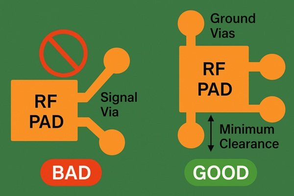
A Closer Look: Managing Via Parasitics in RF Designs
Vias are a necessary evil; mitigating their parasitics is crucial.
- Parasitic Effects:
- Inductance (\(L\)): ~\(0.5 \text{ nH}\) to \(1 \text{ nH}\) for a typical via (0.25mm drill, 1.6mm board). Its impedance (\(X_L = 2\pi fL\)) can be several Ohms at GHz frequencies.
- Capacitance (\(C\)): ~\(0.2 \text{ pF}\) to \(0.5 \text{ pF}\) to nearby planes.
- Stub Length: Unused via barrel portions cause reflections. Stub length should be less than \(1/(10 \times f_{\text{knee}})\).
- Best Practices:
- Grounding Vias: Use multiple vias for SMT ground pads to reduce inductance.
- Via-in-Pad (VIP): Shortest connection, minimizes parasitics, but needs filling/capping (adds cost). Typical filled via diameter 0.2mm-0.3mm.
- Symmetry: For differential pairs.
- Clearance: Maintain minimum distance from signal vias to other conductors (e.g., >0.127mm).
- Signal Vias: Minimize in critical paths. Use adjacent ground vias for return path continuity.
- Component Manufacturer Guidelines: Follow footprint/via recommendations (e.g., \(3 \times 3\) thermal/grounding vias with 0.8mm pitch for QFNs).
Typical Via Parasitics and Mitigation:
| Via Aspect | Parasitic Concern | Typical Value (1.6mm PCB) | Mitigation Strategy |
|---|---|---|---|
| Inductance | Series impedance, ground bounce | \(0.5 \text{ nH}\) - \(1.0 \text{ nH}\) per via | Use multiple vias in parallel for grounds/power, shorter vias (thinner PCB), larger diameter. |
| Capacitance | Shunt loading, impedance discontinuity | \(0.2 \text{ pF}\) - \(0.5 \text{ pF}\) per via | Increase anti-pad diameter, minimize via pad size on non-connecting layers. |
| Stub | Resonance, reflections at high freq. | Length of unused via barrel | Back-drilling, blind/buried vias (more expensive), careful layer assignment. |
| Return Path | Discontinuity for ground current | N/A | Place ground vias close to signal vias when transitioning layers. |
In my work with multi-Gbps signals, managing via transitions was critical, using multiple ground vias alongside signal vias.
Conclusion
In RF PCB design, component placement isn't just about fitting parts; it's a critical engineering step. Prioritizing Functional Bloc Isolation with Controlled Impedance Interconnects and meticulously applying these detailed considerations will pave the way for a successful, high-performing RF product.
-
Understanding the skin effect is crucial for minimizing signal loss in RF applications. Explore this link to deepen your knowledge. ↩
-
Effective current return paths are crucial for RF integrity. This link will provide valuable techniques to enhance your PCB designs. ↩
-
Exploring Ground Plane Management can enhance your PCB design skills, leading to better signal integrity and performance. ↩
-
Identifying feedback mechanisms is key to troubleshooting RF amplifiers. Learn about common issues and effective layout solutions. ↩
-
Understanding RF filter placement can enhance signal integrity and system performance, crucial for effective communication. ↩
-
Impedance matching is essential for optimal filter performance, preventing signal degradation and ensuring efficiency. ↩
-
Learning about thermal vias can significantly improve your PCB's thermal performance, ensuring sensitive components remain stable under load. ↩


