 Skip to content
Struggling with manufacturing holds because of tooling hole issues? These small details can cause big delays, but getting them right is simple once you know the standard specifications.
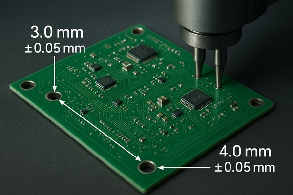
Typically, PCB tooling holes have a diameter of 3.0 mm or 4.0 mm (approximately 118 or 157 mils). A common industry tolerance is ±0.05 mm (±2 mils), a high-precision requirement guided by the principles of IPC-2221 for manufacturability. These non-plated holes are essential for precise mechanical alignment during automated manufacturing, assembly, and testing processes.
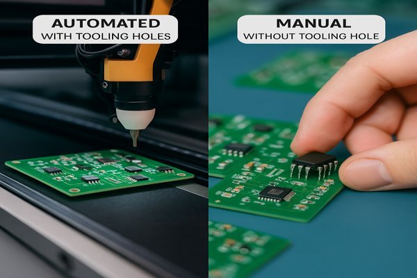
Tooling holes might seem like a minor detail in a complex PCB design, but they are one of the first things a manufacturer looks for. They are the physical interface between your design and the entire automated production line. Ignoring or misplacing them can bring your project to a halt before it even begins. In my nearly 20 years of hardware engineering, from aerospace to medical devices, I've seen simple tooling hole mistakes cause frustrating delays that could have been easily avoided. Let's break down exactly what they are, where they go, and why they are so critical for a smooth transition from design to a finished product.
What is the purpose of a tooling hole on a PCB?
Ever wonder why those simple holes are so important? Using them incorrectly can lead to assembly errors, failed tests, and a lot of wasted time and money.
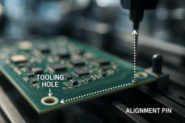
A tooling hole's main purpose is to provide a precise and stable mechanical anchor point. Manufacturing equipment uses these holes to align and secure the PCB for automated processes like component placement, inspection, and testing, ensuring accuracy and repeatability across a production run.
In my experience, especially on high-volume projects like the Tuxedo Keypad at Honeywell, tooling holes were non-negotiable. They serve as the universal registration system for the board as it moves through different machines.
How Tooling Holes Function in Automated Production
These holes are active participants in several critical manufacturing steps:
- Solder Paste Screening: A stencil is laid over the PCB to apply solder paste. Tooling holes ensure the stencil is perfectly aligned, which is critical for preventing solder defects on fine-pitch components.
- Automated Assembly: Pick-and-place machines use tooling pins to lock the PCB into a fixed position, ensuring accurate component placement.
- Automated Optical Inspection (AOI)1: Post-assembly, an AOI machine scans the board. Tooling holes align the board with the machine's camera and the "golden board" reference image.
- In-Circuit Testing (ICT)2: During ICT, the board is pressed onto a "bed of nails" fixture. Tooling holes guarantee every test probe makes a solid connection.
How Tooling Holes Impact Yield and Throughput
The precision provided by tooling holes has a direct, measurable impact on business metrics. A board that is not perfectly stable can cause component shift during placement, especially on fine-pitch BGAs (e.g., 0.4mm pitch). This directly reduces the first-pass yield, increasing rework costs and scrap rates. The table below illustrates the business impact.
| Alignment Method | First-Pass Yield | Throughput (Cycle Time) |
|---|---|---|
| Good (with Tooling Holes) | High; fewer placement errors and solder defects. | High; fast, reliable pin-based machine setup. |
| Poor (No Tooling Holes) | Low; increased rework and scrap due to mis-alignment. | Low; slower cycle times from reliance on less reliable methods. |
Where should tooling holes be placed on a PCB?
Putting tooling holes in the wrong spots can make them useless. This can cause alignment failures and force a costly redesign or manufacturing halt.
Place three tooling holes in a non-symmetrical, triangular pattern, as far apart as possible, typically near the corners of the PCB. This "L-shape" configuration prevents the board from being loaded incorrectly into machinery, ensuring a unique and stable orientation.
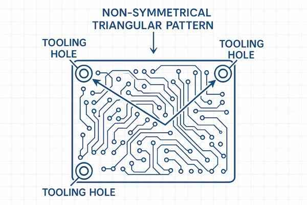
The logic behind the placement is all about eliminating ambiguity and maximizing stability. A three-hole, non-symmetrical pattern provides a single, foolproof orientation, a concept in lean manufacturing known as poka-yoke (mistake-proofing).
Best Practices for Tooling Hole Placement
To get it right every time, follow these specific guidelines:
| Parameter | Recommendation | Rationale |
|---|---|---|
| Pattern | 3 holes in a triangular or "L" shape. | Provides a unique orientation, preventing rotation errors. |
| Location | As far apart as possible, near board corners. | Maximizes the lever arm, providing the most stable alignment. |
| Edge Clearance | At least 3 mm to 5 mm (120-200 mils) from the board edge. | Prevents breakout or damage during drilling and handling. |
| Component Clearance | At least 3 mm (120 mils) from any component or trace. | Prevents interference with assembly equipment or tooling pins. |
Advanced Error-Proofing with Hole Shapes and Sizes
For an even more robust design, make one of the three holes different. This makes it physically impossible to load the board incorrectly.
- Different Size: Use two holes of one size (e.g., 3.0 mm) and a third of a slightly different size (e.g., 3.1 mm). The fixture's pins will match, so the board only fits one way.
- Different Shape: Use two round holes and one slotted or oval-shaped hole. This also creates a unique mechanical key that prevents misorientation.
Placing Tooling Holes on PCB Panels
When tooling holes are on a panel frame, their position relative to depaneling features is critical.
- V-Grooves: Tooling holes must be placed far enough away from V-groove score lines to maintain the panel's structural integrity during assembly. A common rule is to keep the edge of the hole at least 6.35mm (0.25 inches) from the center of any V-groove.
- Mouse Bites3: Ensure the tooling holes do not interfere with the breakout tabs (mouse bites) or the routing path used to separate the boards from the frame.
Should PCB tooling holes be plated or non-plated?
Choosing between plated and non-plated tooling holes seems trivial, but it has a direct impact on manufacturing precision. The wrong choice can compromise the very accuracy you're trying to achieve.
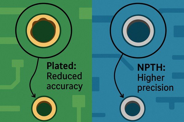
Tooling holes should be specified as Non-Plated Through-Holes (NPTH). Plating adds a layer of copper that is not perfectly uniform, which can slightly alter the hole's final diameter and reduce its dimensional accuracy. NPTH provides a cleaner, more precise hole for mechanical pins.
The primary job of a tooling hole is to provide a precise mechanical interface. The fabrication process and electrical characteristics are key differentiators, as summarized below.
| Feature | Non-Plated (NPTH) - Recommended | Plated (PTH) - Not Recommended |
|---|---|---|
| Dimensional Accuracy | High. Diameter is determined only by the drill bit. | Low. Plating adds an uneven copper layer (20-25 µm). |
| Drilling Stage | After copper plating (final drill stage). | Before copper plating. |
| Electrical Risk | None. The hole is electrically isolated. | High. Can create unintended ground paths if it touches fixtures. |
| Primary Use | Alignment, mounting holes. | Vias, component leads, some mounting holes. |
Designing Copper Clearance for Non-Plated Holes
Even though the hole is unplated, you must define a clearance area in your CAD tool on all copper layers. This prevents adjacent copper fills or traces from being exposed or shorted when the hole is drilled. A safe practice is to define a keep-out area extending 0.25mm (10 mils) from the edge of the drilled hole to any copper feature.
Are tooling holes always necessary for PCB manufacturing?
Engineers often ask if they can skip tooling holes to save space. While tempting for simple boards, skipping them can create significant problems for any automated production process.
For any board intended for automated assembly (SMT) or testing (AOI, ICT), tooling holes are essential. While you might omit them for a single, hand-built prototype, they are a standard requirement for reliable, repeatable, and scalable production.
In my work, I treat tooling holes as a fundamental part of the design-for-manufacturing (DFM) process.
What if Tooling Holes Aren't Possible? 🤔
In rare cases, tooling holes may be impractical. The alignment strategy must then be adapted to the specific PCB technology.
| PCB Type | Primary Alignment Method | Key Considerations & Trade-offs |
|---|---|---|
| Standard Rigid PCB | Tooling Holes + Global Fiducials | Most reliable, cost-effective, and fastest method. |
| High-Density Rigid PCB | Precision Edge Clamping + Advanced Optics | Expensive custom fixtures required. Slower cycle times. |
| Flexible PCB (FPC) | Sprocket Holes on carrier panel + Fiducials | FPC is mounted to a rigid carrier for assembly. Requires special handling. |
What happens if you don't include tooling holes in your design?
Forgetting to add tooling holes is a common mistake for junior engineers. The consequences almost always involve project delays and unexpected costs, right when you're trying to get prototypes made quickly.
If you submit a design without tooling holes, your manufacturer will almost certainly put the job on hold. They will contact you to request a design revision, or offer to add the holes themselves for an extra fee and a longer lead time.
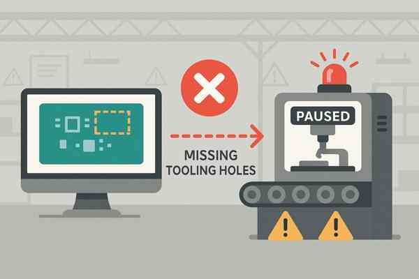
I've been on both sides of this conversation. The impact is real and measurable.
The Ripple Effect on Your Project Timeline
A 1-2 day CAM hold isn't just a small delay. It creates a cascading failure in your project schedule. That two-day slip means the hardware isn't ready for the firmware team to start bring-up. The delayed hardware prevents the mechanical team from performing fit checks. This can ultimately cause you to miss a critical investor demo, a product launch date, or a major trade show, turning a tiny oversight into a significant business problem.
How do tooling holes differ from fiducial marks?
It's easy to confuse tooling holes and fiducial marks since both help with alignment. However, they serve two very different functions, and confusing them can lead to critical manufacturing errors.
Tooling holes are for mechanical alignment; physical pins hold the board in place. Fiducial marks are for optical alignment; machine vision systems use them as reference points to correct for small rotational or positional offsets before placing components.
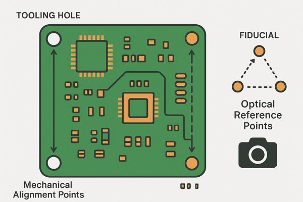
Think of it as a two-step alignment process. The tooling holes do the heavy lifting, and the fiducials provide the fine-tuning.
Using Global and Local Fiducials for Precision
To add another layer of precision, we use two types of fiducials:
- Global Fiducials: 3 marks near the board corners that establish the overall orientation of the PCB.
- Local Fiducials: 1-2 marks placed near a specific component that requires very high placement accuracy, like a fine-pitch BGA. The machine uses these for a final, localized alignment just before placing the chip.
How to Design Reliable Fiducial Marks
For fiducials to work reliably, they must be designed correctly according to industry standards.
| Design Feature | Specification (per IPC guidelines) | Reason |
|---|---|---|
| Construction | Solid copper circle, 1mm to 2mm in diameter. | Provides a clear, defined shape for the vision system. |
| Solder Mask Opening | Diameter should be 2x the fiducial pad diameter. | Creates a high-contrast background ("donut") for easy detection. |
| Keep-out Zone | Area inside the mask opening must be clear of all other items. | Prevents silkscreen or traces from confusing the vision system. |
| Surface Finish4 | ENIG or ENEPIG (flat finishes) are highly preferred. | Avoids light refraction from uneven HASL surfaces. |
For more discussion about fiducial marks, please refer to my article: What Are Fiducial Marks On A PCB?
Conclusion
In summary, tooling holes are a foundational element of Design for Manufacturability. By implementing a robust strategy of three asymmetrically placed, non-plated holes with proper clearances—and complementing them with well-designed global and local fiducials—you eliminate critical manufacturing risks and ensure your project moves from design to production efficiently and reliably.
-
Learn how AOI technology detects assembly defects and ensures PCB quality, helping you understand its crucial role in modern electronics production. ↩
-
Learn how In-Circuit Testing (ICT) ensures PCB quality by detecting assembly defects, helping you understand its critical role in reliable electronics production. ↩
-
Learn how mouse bites are used for PCB separation, their impact on board quality, and best practices to avoid assembly issues. ↩
-
Learn about the different types of conformal coatings used to protect PCBs and their specific properties, benefits, and applications. ↩


