 Skip to content
Struggling with unpredictable RF performance? Your circuit board material choice is often the hidden cause. Several core electrical, thermal, and mechanical properties dictate success or failure in RF designs.
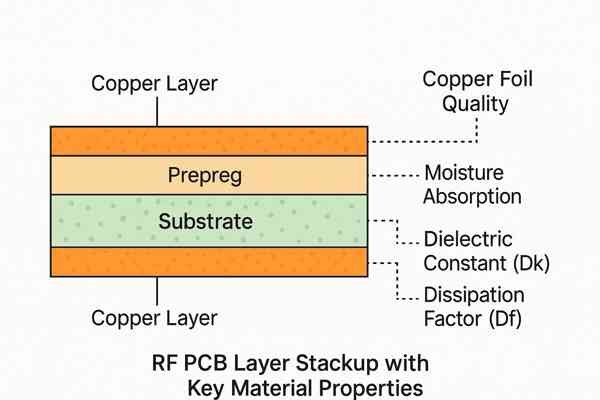
The primary factors driving RF PCB material selection are its dielectric constant (Dk), dissipation factor (Df), the stability of these properties over frequency and temperature, thermal conductivity, moisture absorption, copper foil characteristics, and overall cost versus performance for the specific application.
Choosing the right material for your Radio Frequency (RF) Printed Circuit Board (PCB) can feel like navigating a minefield. Get it wrong, and your brilliant design might sputter and fail. Get it right, and you pave the way for optimal performance. As an engineer with nearly two decades in the trenches, I've seen firsthand how material choices make or break high-frequency projects. Let's explore the critical elements you need to consider.
How Does PCB Material Choice Impact Overall RF Circuit Performance?
Poor RF performance plaguing your project? The PCB material might be silently sabotaging your signal integrity and power efficiency, leading to missed deadlines.
PCB material choice critically impacts RF performance through its influence on signal speed, impedance control, signal loss, power handling, and the stability of these characteristics across operating conditions like frequency, temperature, and humidity.
The material you choose for your RF PCB isn't just a passive substrate; it's an active component in your high-frequency circuits. Its properties directly dictate how signals propagate, how much energy is lost, and how consistently your circuit will behave. As someone who has debugged countless RF systems, I can tell you that overlooking material specs is a common path to frustration. The right material ensures your meticulously designed circuit performs as simulated.
Key Performance Metrics Influenced by Material Choice
The interplay between material properties and RF performance is multifaceted. The stability and predictability of parameters like Dk and Df are paramount for successful RF design. This includes their consistency over frequency, temperature, humidity, isotropic behavior (uniformity in \(X\), \(Y\), and \(Z\) directions), and batch-to-batch consistency from the supplier.
| Material Property | Impact on RF Performance Metric | Why It Matters |
|---|---|---|
| Dielectric Constant (Dk) | Signal propagation speed, characteristic impedance, physical size of circuit elements (e.g., trace width, antenna dimensions). | Crucial for impedance matching, filter tuning, and consistent phase response. Stable Dk ensures predictability. |
| Dissipation Factor (Df)1 | Signal attenuation (dielectric loss), \(Q\)-factor of resonant circuits, overall power efficiency. | Minimizes signal power lost as heat, essential for link budget, LNA noise figure, and efficiency in battery-powered devices. |
| Dk & Df Stability | Consistency of impedance, phase, loss, and resonant frequencies across operating conditions (frequency, temp, humidity). | Ensures reliable performance in real-world scenarios and manufacturability across batches. This is essential for robust designs. |
| Thermal Conductivity (\(k\))2 | Heat dissipation from power components and resistive losses, operational temperature of the circuit. | Prevents overheating, improves component reliability and longevity, allows for higher power handling. |
| Copper Foil Roughness | Conductor loss (especially at high frequencies due to skin effect), effective Dk near the conductor. | Directly impacts insertion loss and can affect phase consistency. Smooth copper is vital for mmWave. |
| Moisture Absorption | Can alter Dk and Df, leading to performance drift in humid environments. | Affects impedance, loss, and overall stability in non-hermetic applications or varying climates. |
| CTE (\(X\), \(Y\), \(Z\) axes) | Solder joint reliability (mismatch with components), dimensional stability of the PCB. | Critical for long-term reliability under thermal cycling, especially with leadless components or large packages. |
I recall a project where an amplifier designed for wideband operation showed unexpected gain roll-off at higher frequencies. The issue was traced back to the material's Dk not being as stable over frequency as the initial datasheet suggested for our specific operating conditions and layout. This highlights why deeply understanding these interactions is vital.
What Is a Key Performance Trade-Off Between FR-4 and RF Laminates?
Need an affordable PCB? FR-4 is tempting, but its RF performance limitations can severely compromise your high-frequency design, leading to signal loss and instability.
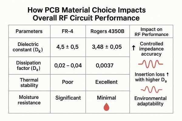
A key trade-off is cost versus high-frequency performance: FR-4 is inexpensive but has high, unstable dielectric losses (Df) and a less stable dielectric constant (Dk) at RF/microwave frequencies compared to specialized RF laminates.
Many of us start our design journey with FR-4. It's the workhorse of the PCB industry – cheap, readily available, and perfectly adequate for digital and low-frequency analog circuits. However, when you venture into the RF domain, especially above \(1\) GHz, the siren song of FR-4's low cost can lead your project onto the rocks. The trade-off isn't just about one parameter; it's a collection of compromises.
Comparing FR-4 and Specialized RF Laminates
| Feature | Standard FR-4 | Specialized RF Laminates (e.g., Rogers RO4000 series) |
|---|---|---|
| Dielectric Constant (Dk)3 | Typically \(4.2 - 4.8\), varies with freq, temp, moisture. | Lower or higher options (e.g., \(2.2 - 10.2\)), very stable. |
| Dk Tolerance | Wide, e.g., \(\pm 10\%\) or loosely specified at RF frequencies. | Tight, e.g., \(\pm 0.05\) or better. |
| Dissipation Factor (Df) | High, e.g., \(0.015 - 0.025\) at \(1\) GHz, worsens with freq. | Low, e.g., \(0.001 - 0.005\), stable with freq. |
| Frequency Stability | Poor for Dk and Df. | Excellent for Dk and Df. |
| Moisture Absorption | Relatively high (e.g., \(0.1\% - 0.5\%\) by weight). | Very low (e.g., less than \(0.05\%\) for many). |
| Thermal Conductivity | Low (approx. \(0.25\) W/mK). | Moderate to good (e.g., \(0.6 - 0.8\) W/mK for some hydrocarbon/ceramics). |
| Glass Transition (\(T_g\)) | \(\approx 130^\circ\text{C} - 180^\circ\text{C}\). | Often \(>280^\circ\text{C}\) for high-performance RF materials. |
| Cost | Low | High (3x to 20x+ FR-4). |
| High-Frequency Use | Generally poor above \(1-2\) GHz for sensitive designs. | Excellent for microwave and mmWave applications. |
The primary appeal of FR-4 is its cost. A standard 4-layer board made with FR-4 might cost, for example, $5-$10 for a small prototype run (per board, depending on size and quantity), whereas a similar board using a Rogers RO4350B material could cost $50-$150 or more. This cost difference is substantial. However, for RF applications, the seemingly attractive price of FR-4 comes with significant performance penalties. Its Df can be an order of magnitude higher than that of good RF laminates. For example, a typical FR-4 might have a Df of \(0.02\) at \(1\) GHz, while a Rogers RO4350B has a Df of \(0.0037\) at \(10\) GHz (Source: Rogers Corporation datasheets). This difference means significantly more signal power is lost as heat in FR-4, especially as frequencies climb.
When Must an RF Design Use a Low Dissipation Factor (Df) Material?
Are high signal losses killing your RF link budget? Your PCB material's dissipation factor might be absorbing too much precious signal power, especially at higher frequencies.
An RF design must use a low dissipation factor (Df) material when minimizing signal attenuation is critical, especially at high frequencies (typically \(>1-2\) GHz), in high-\(Q\) resonant circuits, or for battery-powered devices where power efficiency is paramount.
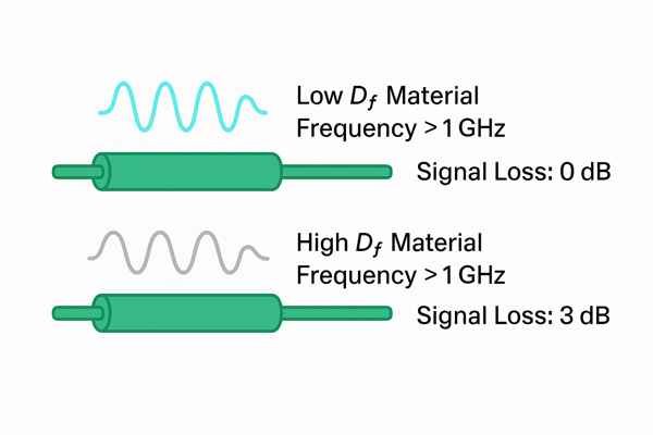
The dissipation factor, often denoted as Df or \(\tan\delta\) (loss tangent), quantifies how much of an electromagnetic wave's energy is absorbed by the dielectric material as it passes through. Think of it as electrical friction. A high Df means more energy is converted into heat within the substrate, leading to weaker signals at the output. In my experience, ignoring Df is a common mistake for engineers transitioning from digital to RF design.
Scenarios Demanding Low Df Materials and Typical Df Values
| Scenario / Material Class | Typical Df (at \(10\) GHz, illustrative) | Reason for Low Df Need | Example Materials (Manufacturer) |
|---|---|---|---|
| General Purpose (FR-4 like) | \(>0.015\) | Not suitable for most demanding RF work above \(1-2\) GHz. | Standard FR-4 |
| Mid-Loss (Improved FR-4/Blends) | \(0.008 - 0.015\) | Marginal for some lower GHz applications, cost-sensitive. | Some "RF-FR4" blends |
| Low-Loss (Hydrocarbon/Ceramic) | \(0.002 - 0.004\) | Good for many microwave apps up to \(20-40\) GHz; LNAs, filters. | RO4350B, TLY-5 (Rogers, Taconic) |
| Ultra Low-Loss (PTFE/Ceramic) | \(<0.002\) | Critical for mmWave, very high-\(Q\) circuits, minimal loss paths. | RT/duroid 5880, CLTE-MW (Rogers) |
High-Frequency Operation: Dielectric losses generally increase with frequency. What might be a negligible loss at \(100\) MHz can become a major issue at \(5\) GHz or \(24\) GHz. For applications above \(1-2\) GHz, low Df materials like Rogers RO3003 (Df \(\approx 0.0013\) at \(10\) GHz) or Panasonic Megtron 6 (Df \(\approx 0.002\) at \(10\) GHz) are chosen. (Source: Manufacturer Datasheets).
High-\(Q\) Resonant Circuits: Filters and oscillators need high Quality (\(Q\)) factors, inversely related to losses. A high Df dampens resonance.
Low-Noise Amplifiers (LNAs): Losses in the input matching network add directly to the LNA's noise figure.
Power-Sensitive Applications: Higher Df means more transmitted power is wasted as heat, reducing battery life.
It's also key to consider the stability of Df over temperature and frequency. A material that boasts a low Df on paper but sees it degrade under operating conditions is not a good choice.
How Does a Material's Dielectric Constant (Dk) Affect RF Trace Width?
Struggling to fit traces in tight RF layouts? The dielectric constant of your PCB material directly influences the physical size of your transmission lines for a given impedance.
A material's dielectric constant (Dk) inversely affects RF trace width for a target impedance: higher Dk values lead to narrower traces, while lower Dk values require wider traces for the same characteristic impedance (e.g., \(50\,\Omega\)).
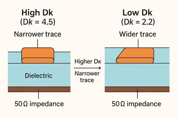
When I'm designing an RF layout, one of the first things I calculate is the trace width needed for my target characteristic impedance, usually \(50\,\Omega\). This calculation heavily depends on the dielectric constant (Dk, also sometimes denoted \(\epsilon_r\)) of the PCB substrate material. Understanding this relationship is fundamental for successful RF design.
Illustrative Trace Widths for \(50\,\Omega\) Microstrip Line (\(H = 0.508\) mm / 20 mils)
| Material Type Example | Typical Dk (at \(10\) GHz) | Approx. Trace Width (\(W\)) for \(Z_0 = 50\,\Omega\) | Notes |
|---|---|---|---|
| PTFE/Woven Glass | \(2.2\) (e.g., Rogers RT/duroid 5880) | \(\approx 1.50\) mm (\(\approx 59\) mils) | Wider traces, lower conductor loss, consumes more space. |
| Hydrocarbon/Ceramic | \(3.48\) (e.g., Rogers RO4350B) | \(\approx 1.10\) mm (\(\approx 43\) mils) | Good balance of performance and manufacturability. |
| FR-4 (High Frequency) | \(4.3\) (Approximate) | \(\approx 0.90\) mm (\(\approx 35\) mils) | Narrower traces, but FR-4 has higher loss and less stable Dk. |
| Ceramic Filled PTFE | \(6.15\) (e.g., Rogers RT/duroid 6006) | \(\approx 0.70\) mm (\(\approx 28\) mils) | Allows for miniaturization, Dk helps shrink component sizes. |
| High Dk Ceramic | \(9.8\) (e.g., Rogers TMM10i) | \(\approx 0.45\) mm (\(\approx 18\) mils) | Significant miniaturization possible, used for patch antennas, filters. |
(Note: These are illustrative values calculated using a standard microstrip formula like \(Z_0 \approx \frac{87}{\sqrt{DK + 1.41}} \ln\left(\frac{5.98H}{0.8W + T}\right)\). Actual widths depend on precise Dk at the design frequency, copper thickness (\(T\)), and should be verified with EDA tools or manufacturer guidelines. For example, source for RO4350B and RT/duroid 5880 Dk values is Rogers Corporation.)
This relationship has practical implications. Narrower traces (from higher Dk) can be beneficial for dense designs but may have higher conductor losses and lower power handling. Wider traces (from lower Dk) generally have lower conductor losses but consume more board space. The choice often involves balancing these factors with the overall circuit requirements. The stability of Dk across frequency and manufacturing tolerances is crucial because variations will directly impact the achieved trace impedance.
Why Is Stable Dk Important for Reliable RF Circuit Operation?
Are your RF circuits performing erratically across different units or conditions? Unstable dielectric constant (Dk) in your PCB material could be the culprit, causing unpredictable impedance and phase shifts.
A stable dielectric constant (Dk) is crucial for reliable RF operation because it ensures consistent characteristic impedance, predictable signal propagation delays, and stable filter/coupler performance across frequency, temperature, humidity, and manufacturing batches.
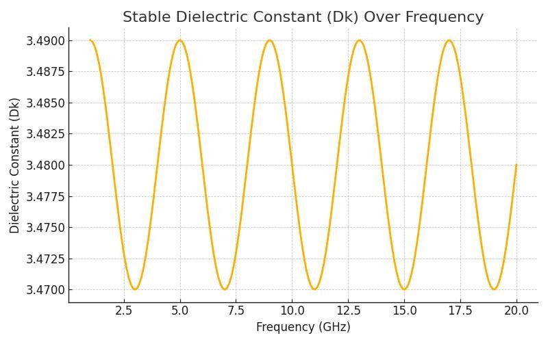
As I've emphasized before, it's not just about having a low Dk; the stability and predictability of this parameter are often far more critical for robust RF designs. Imagine designing a finely tuned filter. If the Dk of your substrate material shifts with temperature or from one PCB batch to another, your filter's center frequency and bandwidth will drift. This is a nightmare I've troubleshooted more than once.
Sources of Dk Instability and Their Impact
| Source of Instability | Typical Variation/Concern | Impact on RF Performance | Mitigation Strategy |
|---|---|---|---|
| Frequency | Dk can decrease or increase with frequency. | Impedance changes over bandwidth, filter detuning, phase errors in broadband signals. | Select materials with flat Dk vs. frequency curve (e.g., Rogers RO4000 series). |
| Temperature | Dk changes with temperature (described by \(TCD_k\)). | Performance drift in varying thermal environments, critical for outdoor or high-power devices. | Choose materials with low \(TCD_k\) (e.g., some PTFE or specialized hydrocarbon ceramics). |
| Humidity/Moisture | Moisture absorption increases effective Dk. | Unpredictable performance in humid conditions, especially for non-hermetic assemblies. | Use low moisture absorption materials (e.g., PTFE, LCP). |
| Batch-to-Batch Variation | Dk varies between different production lots of material. | Inconsistent performance of manufactured units, yield issues in mass production. | Work with reputable suppliers with tight process control; this is essential for consistency. |
| Anisotropy (\(X, Y, Z\) Dk) | Dk differs in \(X\), \(Y\), and \(Z\) axes. | Affects designs with vertical structures (e.g., broadside couplers) or non-aligned traces. | Choose isotropic materials or account for anisotropy in design. |
For example, Rogers RO4350B material has a specified \(TCD_k\) of about \(+40\) ppm/°C (Source: Rogers Corporation). For a Dk of \(3.48\), a \(100^\circ\text{C}\) temperature change could alter Dk by approximately \(3.48 \times 40 \times 10^{-6} \times 100 = 0.0139\). While seemingly small, this can be significant for very sensitive circuits. Ensuring Dk stability often means selecting higher-quality RF laminates where manufacturers invest in material science and process control.
What Thermal Property of a PCB Material Is Key for High-Power RF?
Designing high-power RF amplifiers and concerned about overheating? The PCB material's ability to dissipate heat is crucial, and one thermal property stands out for managing this effectively.
For high-power RF applications, thermal conductivity (\(k\)) is the key thermal property of a PCB material, as it dictates how efficiently heat generated by active devices and conductor losses can be spread and removed from the board.
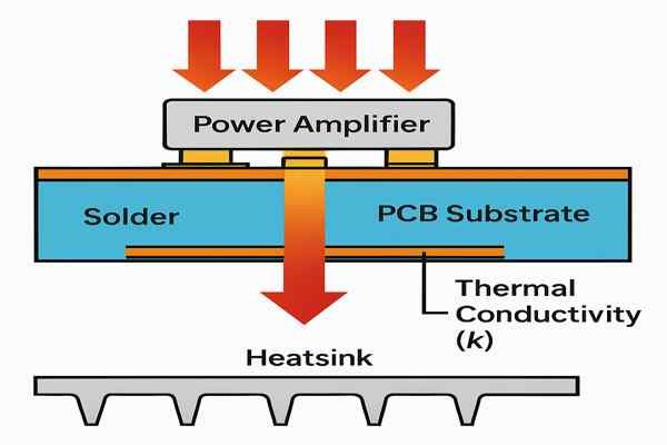
When you're pushing a lot of RF power through a circuit, components like power transistors and even the transmission lines themselves generate significant heat. If this heat isn't managed effectively, temperatures can rise, leading to performance degradation or failure. I’ve seen designs where inadequate thermal management caused amplifiers to fail prematurely during field tests. The PCB material plays a vital role here. While other thermal properties like Glass Transition Temperature (\(T_g\)) and Decomposition Temperature (\(T_d\)) are important, thermal conductivity (\(k\)) directly impacts operational temperature.
Thermal Conductivity (\(k\)) Comparison for Various PCB Materials
| Material Type | Typical Thermal Conductivity (\(k\)) (W/mK) | Suitability for Power Applications |
|---|---|---|
| Standard FR-4 | \(0.25 - 0.35\) | Poor; suitable for low power only. Heat spreading is minimal. |
| FR-4 with Thermal Vias | Effective \(k\) improves locally | Better than standard FR-4, but still limited by bulk material. |
| Hydrocarbon/Ceramic (e.g., Rogers RO4350B)4 | \(0.6 - 0.8\) (e.g., RO4350B is \(\approx 0.62\) W/mK) | Moderate; suitable for medium power RF. Ceramic fillers enhance \(k\). (Source: Rogers Corporation) |
| PTFE/Ceramic (e.g., Rogers RT/duroid 6002) | \(0.4 - 1.0+\) (e.g., RT/duroid 6002 is \(\approx 0.48\) W/mK, some others higher) | Variable; some tailored for high power with higher \(k\). (Source: Rogers Corporation) |
| Metal-Backed PCB (IMS/MCPCB Dielectric) | \(1.0 - 7.0+\) (for the thin dielectric layer) | Excellent; metal base (Al or Cu) provides very high overall heat dissipation. |
| Aluminum (Reference) | \(\approx 205\) | Used as base in IMS/MCPCBs. |
| Copper (Reference) | \(\approx 390\) | Used for traces, ground planes, and as base in some IMS/MCPCBs. |
Using a material with higher thermal conductivity can reduce the junction temperature of active devices, improving their reliability and allowing them to operate at higher power levels. It also helps in maintaining a more uniform temperature across the board, which can be beneficial for the stability of other temperature-sensitive parameters like Dk. In critical designs, thermal simulation is often performed, and the material's thermal conductivity is a key input.
How Does PCB Material Moisture Absorption Affect RF Signals?
Noticing RF performance degradation in humid environments? The moisture absorbed by your PCB material could be altering its dielectric properties and increasing signal losses.
PCB material moisture absorption negatively affects RF signals by increasing both the dielectric constant (Dk) and the dissipation factor (Df) of the material, leading to impedance shifts, increased signal loss, and phase variations.
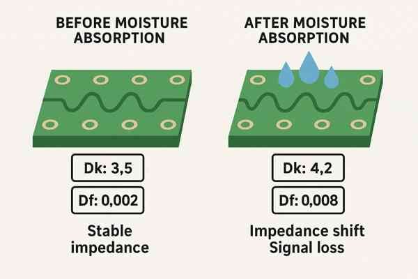
Water is not a friend to high-frequency circuits. When PCB materials absorb moisture from the surrounding environment, their electrical characteristics can change significantly. This is a subtle but critical factor that I always consider, especially for equipment destined for deployment in uncontrolled or humid environments. The stability of material properties is directly challenged by moisture.
Moisture Absorption and Its Impact on Different PCB Materials
| Material Type | Typical Moisture Absorption (\(\%\) by weight, 24hr immersion) | Impact on Dk in Humid Conditions | Impact on Df in Humid Conditions | Overall Stability in Humidity |
|---|---|---|---|---|
| Standard FR-4 | \(0.1\% - 0.5\%\) (some up to \(0.8\%\)) | Significant Increase | Significant Increase | Poor |
| High-Performance FR-4 / Blends | \(0.05\% - 0.2\%\) | Moderate Increase | Moderate Increase | Fair |
| Hydrocarbon/Ceramic (e.g., RO4000 series) | \(\approx 0.05\% - 0.06\%\) (e.g., RO4350B is \(0.06\%\)) | Low Increase | Low Increase | Good (Source: Rogers Corp.) |
| PTFE-based (e.g., RT/duroid series) | less than \(0.02\%\) (e.g., RT/duroid 5880 is \(0.02\%\)) | Negligible Increase | Negligible Increase | Excellent (Source: Rogers Corp.) |
| Liquid Crystal Polymer (LCP) | \(\approx 0.02\% - 0.04\%\) | Very Low Increase | Very Low Increase | Excellent |
(Moisture absorption values are typically per IPC-TM-650, Method 2.6.2.1 or similar standards.)
The effects are clear: water's high Dk (around \(70-80\)) and lossiness will skew the performance of materials that readily absorb it. For applications requiring stable performance regardless of humidity, selecting a material with low moisture absorption, like PTFE or LCP, is crucial. In some of my past projects for outdoor equipment, switching to a low-absorption material solved intermittent field issues that were eventually traced back to humidity changes affecting the circuit tuning.
For mmWave PCBs, What Specific Material Trait Is Most Vital?
Venturing into millimeter-wave frequencies (\(30-300\) GHz)? At these ultra-high frequencies, one material characteristic becomes overwhelmingly critical for minimizing losses and ensuring predictable performance.
For mmWave PCBs, extremely low and stable dissipation factor (Df) is arguably the most vital material trait, followed closely by a tightly controlled and stable dielectric constant (Dk) and very smooth copper foil.
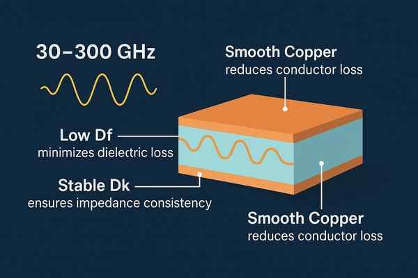
As we push into the millimeter-wave (mmWave) spectrum, the wavelength of signals becomes incredibly short, and even minute imperfections or suboptimal material properties can lead to severe performance degradation. While many factors matter, the impact of dielectric losses (\(\text{Loss (dB/inch)} \propto f \cdot \sqrt{DK} \cdot DF\)) becomes magnified. I've learned that what works at \(5\) GHz can be a complete disaster at \(60\) GHz if material choices aren't carefully re-evaluated.
Key Material Requirements for mmWave PCBs
| Material Trait | Target Value/Characteristic | Why It's Critical for mmWave | Example Materials (Suppliers) |
|---|---|---|---|
| Dissipation Factor (Df) | Extremely Low (e.g., \(<0.002\text{, ideally } <0.0015\) at target freq.) | Dielectric loss is proportional to frequency; becomes dominant loss factor at mmWave. | Rogers CLTE-MW, Taconic TLY series |
| Dk Stability (vs Freq/Temp) | Very High; low \(TCD_k\); flat Dk vs. frequency. | Tiny wavelength means small Dk shifts cause large phase errors & impedance variations. | Rogers RO3003, Panasonic Megtron 7 |
| Dk Tolerance & Uniformity | Very Tight (e.g., \(\pm 0.02\) or better); Isotropic. | Ensures consistent device-to-device performance and predictability of distributed elements. Isotropic Dk is a critical consideration. | High-end PTFE/ceramics, LCP |
| Copper Foil Roughness5 | Ultra-Smooth (e.g., \(R_q < 0.5\) µm, VLP/ULP/HVLP copper) | Skin depth is sub-micron; rough copper significantly increases conductor loss. Crucial for mmWave. | Specific foils from copper suppliers |
| Substrate Thickness Tolerance | Very Tight (e.g., \(\pm 5\%\) or better, down to \(\pm 1-2\%\) for some). | Directly impacts impedance control and phase consistency, more critical with smaller features. | Precision laminates |
At mmWave frequencies, even a material with a Df considered "good" at lower microwave frequencies (e.g., \(0.004\)) can result in unacceptable losses. Materials chosen for mmWave applications, such as Rogers CLTE-MW™ (Df \(\approx 0.0015\) at \(40\) GHz) or Taconic TLY-5 (Df \(\approx 0.0009\) at \(10\) GHz, though Df tends to increase with frequency), strive for the lowest possible Df. (Source: Manufacturer Datasheets). The interaction of the dielectric with copper foil roughness also becomes paramount.
How Does Copper Foil Roughness Influence RF Insertion Loss?
Are you experiencing higher-than-expected insertion loss in your RF circuits, especially at high frequencies? The roughness of the copper foil on your PCB might be a significant contributing factor.
Copper foil roughness primarily increases RF insertion loss by exacerbating conductor losses due to the skin effect and by potentially increasing the effective dissipation factor (Df) of the dielectric near the copper surface, especially at microwave and mmWave frequencies.
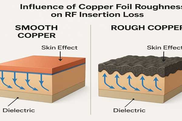
It's important to remember that the interaction between dielectric and copper roughness is critical. When I first started in RF design, I primarily focused on the dielectric properties. However, as frequencies climbed in my projects, I learned that the characteristics of the copper foil, particularly its surface roughness, play an increasingly crucial role in determining overall circuit performance. The skin depth (\(\delta\)) is given by \(\delta \approx \frac{66}{\sqrt{f}}\) (where \(f\) is in Hz and \(\delta\) is in µm). At \(1\) GHz, \(\delta \approx 2.09\) µm; at \(10\) GHz, \(\delta \approx 0.66\) µm; and at \(100\) GHz, \(\delta \approx 0.21\) µm.
Comparison of Copper Foil Types and Their Impact
| Copper Foil Type | Typical Profile | Avg. Roughness (\(R_q\) or \(R_z\)) | Skin Depth Example (at \(10\) GHz: \(\approx 0.66\) µm) | Impact on High-Frequency Loss |
|---|---|---|---|---|
| Standard ED | High Profile (HP) / Standard Profile (SP) | \(R_z\): 5-10+ µm; \(R_q\): 1-3 µm | Roughness \(>\) Skin Depth | Significant increase in loss due to longer current path. |
| Reverse Treated (RTF) | Lower Profile than Standard ED | \(R_z\): 3-7 µm; \(R_q\): 0.8-1.5 µm | Roughness often \(>\) Skin Depth | Moderate improvement over Standard ED. |
| VLP (Very Low Profile) | Very Low Profile | \(R_z\): \(\approx\) 2-3 µm; \(R_q\): \(\approx\) 0.4-0.8 µm | Roughness comparable to Skin Depth | Good reduction in loss compared to ED. Common for microwave. |
| ULP/HVLP (Ultra/Hyper Low Profile) | Ultra/Hyper Very Low Profile / No Profile | \(R_z\): \(<\)1.5 µm; \(R_q\): \(<\)0.4 µm | Roughness \(<\) Skin Depth | Best performance; minimal added loss. Essential for mmWave. |
(Roughness values are typical. \(R_z\) is 10-point mean roughness, \(R_q\) is RMS roughness. IPC-4562 classifies foils.)
If the copper surface is rough, with peaks and valleys comparable to or larger than the skin depth (\(\delta\)), the current effectively travels a longer path. This increased path length leads to higher resistive losses. Some models also suggest that the increased field concentration around rough copper can increase apparent dielectric loss near the conductor. Using smoother copper, like VLP or ULP, can significantly reduce insertion loss, especially above a few GHz. For instance, at \(20\) GHz, moving from standard ED copper to a smoother profile might save \(0.1 \text{ to } 0.2\) dB/inch or more.
What Is the Primary Cost Driver When Selecting RF PCB Materials?
Trying to balance RF performance with project budget? The choice of PCB material is a major cost factor, but what specifically makes some RF laminates so much more expensive?
The primary cost driver when selecting RF PCB materials is the raw material composition and manufacturing complexity of the laminate itself, with low-loss dielectrics (like PTFE, advanced ceramics, and specialized resins) and controlled manufacturing processes commanding premium prices.
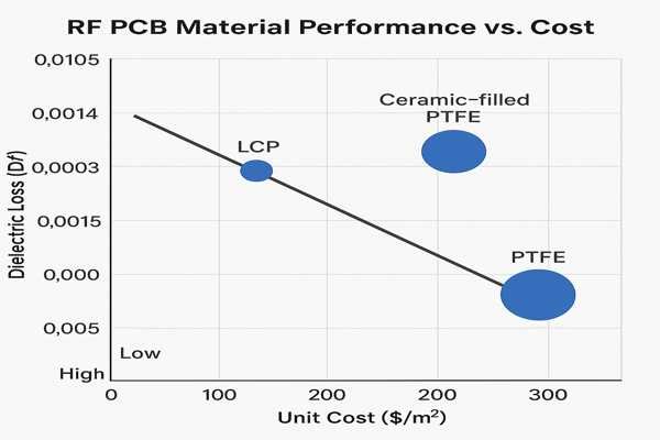
Whenever I'm planning a new RF project, the budget discussion inevitably comes up. While FR-4 is very inexpensive, high-performance RF laminates can increase PCB costs significantly. It's important to understand why these materials cost more so you can make informed trade-offs.
Relative Cost and Characteristics of RF PCB Material Categories
| Material Category | Key Dielectric(s) | Typical Df (at \(10\) GHz) | Dk Stability | Relative Cost per Sq. Foot | Primary Use Cases |
|---|---|---|---|---|---|
| Standard FR-4 | Epoxy Resin, Woven Glass | \(>0.015\) | Poor | ($5-$10) | Low frequency (\(<1\) GHz), non-critical RF, prototyping where loss is tolerable. |
| Enhanced FR-4 / Blends | Modified Epoxy/Resin Systems | \(0.008 - 0.015\) | Fair | ($15-$30) | Cost-sensitive RF up to few GHz, less demanding applications. |
| Hydrocarbon / Ceramic | Hydrocarbon Resins, Ceramic Fillers | \(0.002 - 0.004\) | Good | ($30-$100+) | Microwave (up to \(\approx 40\) GHz), LNAs, filters, antennas (e.g., Rogers RO4000 series). |
| PTFE / Ceramic or Glass | PTFE, Ceramic/Microfiber Glass | \(<0.001 - <0.002\) | Excellent | ($50-$150+) | High-performance microwave, mmWave, low PIM (e.g., Rogers RT/duroid series). |
| Advanced Composites (LCP) | Liquid Crystal Polymer | \(<0.002\) | Excellent | ($100-$300+) | mmWave, high-frequency packaging, flexible RF circuits. |
(Cost estimates are very approximate and can vary widely based on supplier, volume, and specific grade.)
The tight tolerances on Dk, Df, thickness, and the stability of these parameters are critical and require sophisticated manufacturing and QC, adding to the cost. Specialized fillers and smoother copper foils also contribute. For instance, a small 2-layer prototype PCB (e.g., 10cm x 10cm) might cost $10-$20 on FR-4. The same board using Rogers RO4350B could cost $70-$150, and if it's a more exotic mmWave material, it could be $300-$500 or more.
How Does Material CTE Mismatch Affect RF PCB Solder Joint Reliability?
Worried about solder joint failures in your RF assemblies, especially under temperature cycling? The Coefficient of Thermal Expansion (\(\text{CTE}\)) mismatch between your PCB material, components, and solder can be a major stressor.
Material \(\text{CTE}\) mismatch between the PCB substrate, mounted components (especially ceramic ones like chip resistors or BGAs), and solder can induce significant mechanical stress during temperature changes, leading to solder joint fatigue and eventual failure, thus impacting long-term reliability.
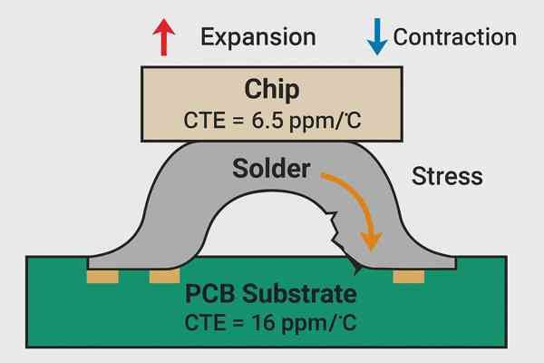
Reliability is paramount in any electronic design, and for RF systems that might operate in varying thermal environments, solder joint integrity is a key concern. I've seen my share of field failures that were ultimately traced back to stress caused by \(\text{CTE}\) mismatches, particularly with larger or leadless components. The Coefficient of Thermal Expansion6 (\(\text{CTE}\)) is typically measured in parts per million per degree Celsius (ppm/°C).
Typical \(\text{CTE}\) Values and Mismatch Concerns
| Material | Typical \(\text{CTE}\) (\(X-Y\) axis) (ppm/°C) | Typical \(\text{CTE}\) (\(Z\)-axis) (ppm/°C) | Notes on Mismatch Concerns |
|---|---|---|---|
| Copper | \(\approx 17\) | \(\approx 17\) | Reference for traces and planes. |
| FR-4 Laminate | \(14 - 18\) | \(50 - 70+\) (below \(T_g\)) | Significant \(X-Y\) mismatch with ceramics. High \(Z\)-axis \(\text{CTE}\) stresses plated through-holes. |
| RF Hydrocarbon/Ceramic (e.g., RO4000) | \(10 - 16\) (e.g., RO4350B \(\approx 11\)) | \(30 - 50\) | Better \(X-Y\) match to copper. \(Z\)-axis still higher than \(X-Y\). (Source: Rogers Corp.) |
| RF PTFE/Ceramic (e.g., RT/duroid 6002) | \(12 - 25\) (e.g., RT/duroid 6002 \(\approx 16\)) | \(20 - 30\) | Some can be tailored for good \(X-Y\) match to copper or alumina. (Source: Rogers Corp.) |
| Alumina Ceramic (\(Al_2O_3\)) | \(\approx 6 - 8\) | \(\approx 6 - 8\) | Common for chip components; large mismatch with FR-4. |
| Silicon (Si) Die | \(\approx 2.6 - 3\) | \(\approx 2.6 - 3\) | Very low \(\text{CTE}\); mismatch with most substrates for large die. |
| Solder (SAC305 Lead-Free) | \(\approx 21 - 23\) | \(\approx 21 - 23\) | Its ductility helps absorb some stress, but fatigue is still a concern. |
When an assembly with mismatched \(\text{CTE}\)s undergoes temperature cycling (e.g., \(-40^\circ\text{C to } +85^\circ\text{C}\)), each material expands or contracts differently, creating stress at solder joints. For example, a ceramic chip (\(\text{CTE} \approx 7\) ppm/°C) on FR-4 (\(\text{CTE} \approx 16\) ppm/°C) will experience significant stress. RF circuits often use leadless SMDs and BGAs, which are particularly susceptible. Choosing PCB materials with \(\text{CTE}\) values more closely matched to critical components or using materials with low \(Z\)-axis expansion is a critical design consideration.
Conclusion
Selecting the right RF PCB material involves balancing dielectric properties, thermal performance, mechanical stability, and cost. Prioritize stable Dk/Df, low loss, and suitable thermal/mechanical traits for your specific application.
-
Exploring the impact of Df on RF performance can help in minimizing signal loss and improving efficiency, essential for high-performance applications. ↩
-
Thermal conductivity plays a key role in heat management and reliability of RF circuits, making it essential for effective design and longevity. ↩
-
Dk is a key parameter influencing signal propagation and overall circuit performance in RF applications. ↩
-
Learn about Rogers RO4350B's thermal properties and its suitability for medium power RF applications, enhancing your design choices. ↩
-
Learn about the significance of copper foil roughness in reducing conductor loss at mmWave frequencies. ↩
-
Understanding CTE is crucial for selecting materials in electronics to prevent stress and failure during temperature changes. ↩


