 Skip to content
Struggling with RF PCB projects hitting snags? Unclear fabrication instructions cause costly delays and performance issues. I've found that getting it right the first time hinges on providing precise information.
To ensure smooth RF PCB fabrication, you absolutely need to provide complete Gerber files, a detailed layer stack-up diagram, specific RF material requirements, clear controlled impedance details, comprehensive fabrication notes, and any special testing needs like Time Domain Reflectometry (TDR).

Getting an RF printed circuit board (PCB) made correctly involves more than just sending a design file. High-frequency circuits are very sensitive to physical characteristics of the board. Missing even small details can lead to a board that doesn’t perform as expected, or worse, doesn’t work at all. I’ve learned over my nearly 20 years as a hardware engineer that being meticulous with the information I provide to the fabrication house is key. Let's explore the critical details that I always double-check.
What Files Must Be Sent For RF PCB Fabrication And Assembly?
Tired of your PCB fab house asking for missing files? I know I've been there. Incomplete design data is a common cause of production holds, slowing everything down. Ensure you send everything they need upfront.
For RF PCB fabrication and assembly, you must send Gerber files (for all copper layers, solder mask, silkscreen, paste stencil, and board outline), an NC drill file, a detailed stack-up drawing, a comprehensive Bill of Materials (BOM), and pick-and-place data.
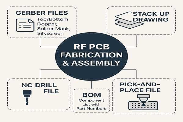
When I prepare a package for an RF PCB, I make sure it’s complete to avoid any back-and-forth. This means more than just the basics.
Core Fabrication Files: Beyond the Gerbers
The Gerber files1, in RS-274X extended format, are the bedrock, defining copper layers, solder mask, silkscreen, and paste. However, for complex RF boards, an ODB++ package can be superior. It's an intelligent format that bundles design data, reducing misinterpretation risks. The NC (Numerical Control) drill file (Excellon format) is non-negotiable for hole data.
Essential Complements for Clarity
I always include an IPC-356 netlist. This allows the fab house to perform an electrical test comparing the Gerbers against my intended connectivity, crucial for catching errors before etching. Assembly drawings are vital, especially for polarized RF components like diodes or directional couplers where incorrect orientation means a non-functional board.
BOM and PNP: Precision for RF Components
The Bill of Materials (BOM)2 for RF needs extra precision. It's not just about part numbers; for passive components, I explicitly list required tolerances (e.g., \(1\%\) for resistors in a filter) and frequency ratings. Pick-and-Place (PNP) data must be exact, especially the rotation for RF footprints which can be asymmetrical.
Here's a snippet of how I might structure critical RF BOM entries:
| Ref Des | MPN | Description | Value | Tolerance | Freq. Rating |
|---|---|---|---|---|---|
| C12 | ATC100B1R0BT500XT | Capacitor, RF/Microwave, NP0 | \(1.0 \text{ pF}\) | \(\pm 0.1 \text{ pF}\) | \(500 \text{ MHz}\) |
| L3 | Coilcraft0402CS-2N2XJLW | Inductor, Wirewound Ceramic | \(2.2 \text{ nH}\) | \(\pm 5\%\) | \(>6 \text{ GHz}\) |
| R7 | RCPF040210R0FKEA | Resistor, Thick Film | \(10 \Omega\) | \(\pm 1\%\) | N/A |
This level of detail prevents ambiguity and ensures the right components are sourced and placed.
Why Is An Exact PCB Layer Stack-up Diagram Vital For RF Boards?
Are your RF circuits underperforming? I’ve seen it happen when the stack-up is ambiguous. An ambiguous stack-up can ruin impedance control and signal integrity. A precise diagram is absolutely essential for high-frequency success.
An exact PCB layer stack-up diagram is vital for RF boards because it defines material types, dielectric constants (\(\epsilon_{r}\)), loss tangents (\(\tan\delta\)), and layer thicknesses—all critical for achieving target impedances and minimizing signal loss at RF frequencies.
The layer stack-up is the heart of an RF PCB's performance. It's not just a mechanical drawing; it's an electrical specification.
Fundamental Parameters Dictated by Stack-up
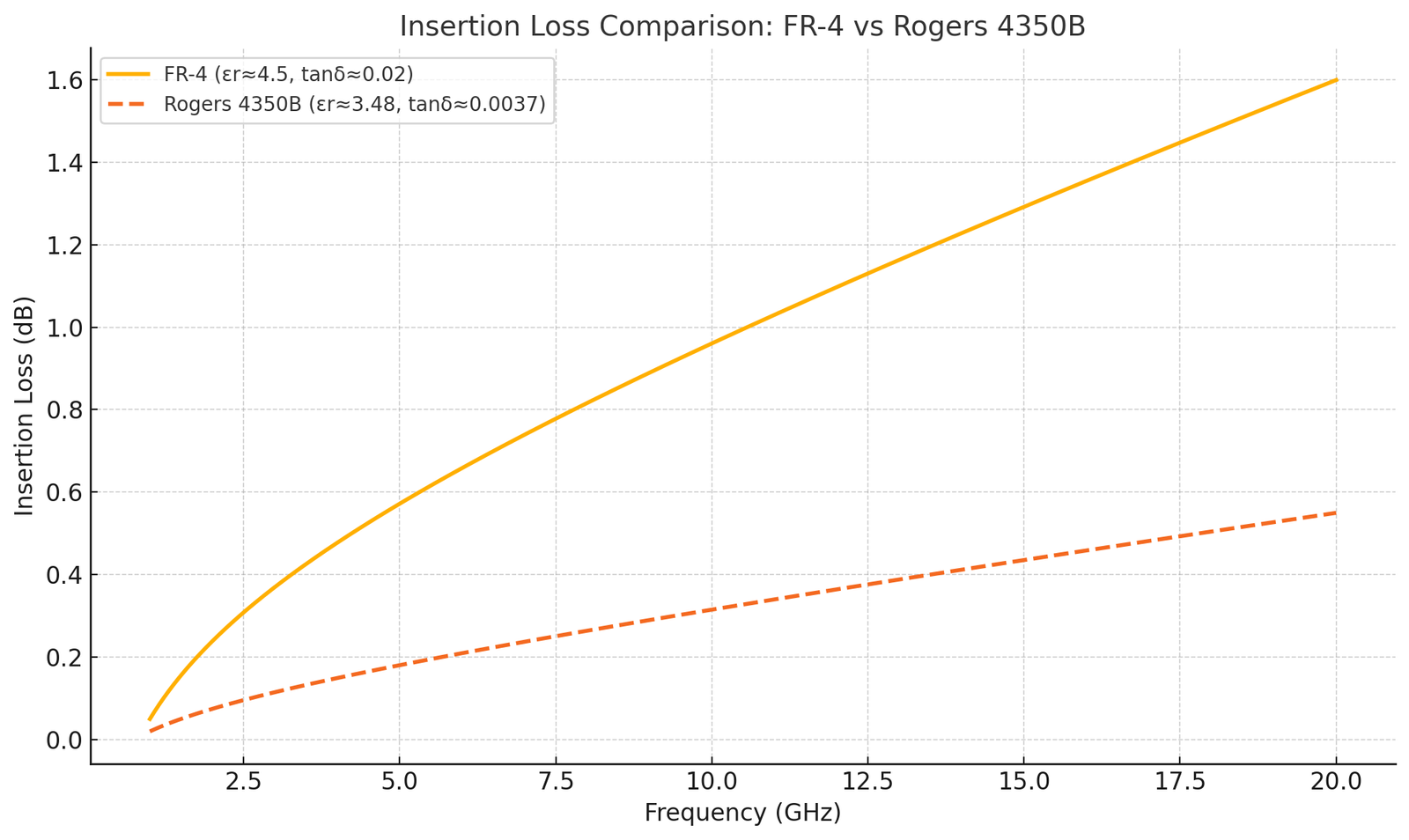
The dielectric constant3 (\(\epsilon_{r}\)) and loss tangent (\(\tan\delta\)) of the materials are paramount. For instance, Rogers RO4350B has a design \(\epsilon_{r}\) of \(3.48\) and \(\tan\delta\) of \(0.0037\) at \(10 \text{ GHz}\) (Source: Rogers Corporation datasheets). Variations in these values, which can be frequency-dependent, directly affect the phase velocity of signals and the amount of signal lost (attenuation) as they travel. Layer thicknesses, for both dielectrics and copper, are critical for achieving characteristic impedance targets. Even small deviations can shift impedance values, leading to reflections and degraded performance. Tolerances for these parameters (e.g., per IPC-4101) must be tight.
Copper Properties: Critical for High-Frequency Performance
Copper isn't just copper at RF. I specify copper weight (e.g., \(0.5 \text{ oz}\) or \(\approx 17.5 \text{ µm}\), \(1 \text{ oz}\) or \(\approx 35 \text{ µm}\)) and type (Electrodeposited - ED, or Rolled-Annealed - RA). RA copper is smoother and often preferred for very high frequencies. Copper surface roughness (quantified by \(R_{q}\) or \(R_{z}\)) is hugely important, especially above \(\approx 20 \text{ GHz}\). Rougher copper increases the effective path length for current due to the skin effect, significantly increasing conductor losses. I might specify a VLP (Very Low Profile) copper with \(R_{q} < 0.8 \text{ µm}\).
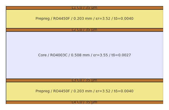
Example RF Stack-up Detail
| Layer | Material | Mfr/Grade | \(\epsilon_{r} \text{ (@10 GHz)}\) | \(\tan\delta \text{ (@10 GHz)}\) | Thick. (\(\text{µm}\)) | Copper (\(\text{oz}\)) | Copper Finish |
|---|---|---|---|---|---|---|---|
| 1 | Copper | \(35\) | \(1\) | (e.g., VLP) | |||
| Dielectric | Rogers RO4350B | \(3.48\) | \(0.0037\) | \(152\) | |||
| 2 | Copper | \(35\) | \(1\) | ||||
| Prepreg | Rogers 4450F | \(3.54\) | \(0.004\) | \(102\) | |||
| 3 | Copper | \(35\) | \(1\) | ||||
| Dielectric | Rogers RO4350B | \(3.48\) | \(0.0037\) | \(152\) | |||
| 4 | Copper | \(35\) | \(1\) | (e.g., VLP) |
This detailed table, part of my fab drawing, leaves no room for error.
What Key Details Belong In RF PCB Fabrication Notes?
Frustrated by RF boards not meeting spec? I've learned that vague notes leave too much to interpretation. Clear, concise fabrication notes prevent costly mistakes and ensure the desired RF performance.
Key details in RF PCB fabrication notes include impedance control requirements (listing specific traces and their target impedances with tolerances), specific material callouts (cross-referencing the stack-up), via fill/plug instructions if any, chosen surface finish, and any specific testing or inspection criteria like TDR coupon testing.
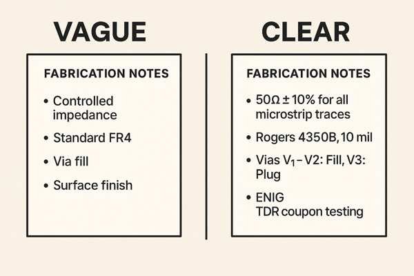
Fabrication notes are my direct line of instruction to the manufacturer, covering aspects beyond the graphical data.
Defining Electrical Performance Criteria
I always include a prominent note cross-referencing the detailed impedance table (see next section) and specifying that TDR test coupons are mandatory. For material callouts, I reiterate the exact laminate and prepreg types from the stack-up diagram, often stating "No substitutions allowed unless explicitly approved in writing by [My Company/Name]." This prevents unwelcome surprises with "equivalent" materials that aren't equivalent at RF.
Physical and Assembly Considerations
Solder mask specifications are critical. Beyond type (LPI) and color, I specify the required solder mask relief around RF pads (e.g., \(75-100 \text{ µm}\) pullback from copper edge) to minimize its dielectric loading effect. Silkscreen constraints involve keeping it off all pads and a minimum clearance (e.g., \(50 \text{ µm}\)) from RF traces to prevent any capacitive or material interaction. For annular ring requirements, I specify compliance with IPC-6012 Class 24 or 3, ensuring robust via connections, vital for RF grounds.
Quality and Compliance
I typically specify manufacturing to IPC-6012 Class 2 as a baseline. For high-reliability or very high-frequency boards, I might require IPC-6012 Class 3/A, which imposes tighter tolerances and inspection criteria.
Here's a checklist example for fabrication notes:
| Category | Detail | Example Specification |
|---|---|---|
| Standard | IPC Class | IPC-6012 Class 2 (or Class 3 if needed) |
| Materials | Laminate/Prepreg | See Stack-up Diagram; No substitutions |
| Impedance Control | Reference Table & Testing | See Impedance Table; TDR Coupons Mandatory |
| Solder Mask | Type, Clearance for RF pads | Green LPI; \(0.075 \text{ mm}\) min. clearance from RF copper features |
| Silkscreen | Color, Min Line, Clearance | White; \(0.1 \text{ mm}\) min line; No silkscreen on pads/RF traces |
| Via Treatment | Plugging/Filling | See specific notes if via-in-pad or filled vias used |
| Surface Finish | Type | ENIG, \(0.05-0.1 \text{ µm Au}\) over \(3-6 \text{ µm Ni}\) |
How Are RF Controlled Impedance Needs Best Given To A Fab House?
Worried your RF signals won't perform as designed? I certainly have been. Unclear impedance instructions lead to mismatches and reflections. Provide clear, unambiguous specifications for predictable results.
RF controlled impedance needs are best given through a table in the fabrication drawing, specifying trace widths, target impedance values (e.g., \(50 \Omega\), \(75 \Omega\), \(100 \Omega\) differential) with tight tolerances (e.g., \(\pm 5\%\) or \(\pm 7\%\)), and their corresponding layers and reference planes.
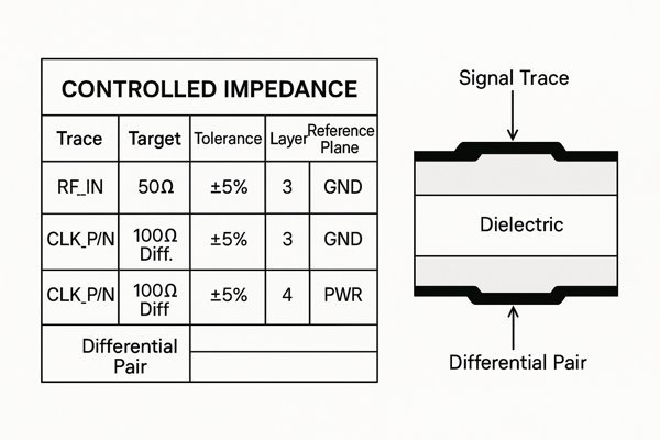
Clear communication of impedance requirements is non-negotiable for RF PCBs.
The Impedance Table: A Contract for Performance
An impedance table on the fabrication drawing is the most effective way. It should be comprehensive. My tables typically include:
| Net Name(s) / Trace ID | Layer | Type | Target \(Z (\Omega)\) | Calculated Width (\(\text{µm}\)) | Dielectric Above/Below (\(\text{µm}\)) | Ref Layer(s) | Tolerance (\(\%\)) |
|---|---|---|---|---|---|---|---|
| RF_IN | 1 | Single-End | \(50\) | \(285\) | \(152\) (D1) | 2 (GND) | \(\pm 5\) |
| CLK_P, CLK_N | 3 | Differential | \(100\) | \(150\) (Width), \(200\) (Gap) | \(102\) (P2) | 2, 4 (GND) | \(\pm 7\) |
| ANT_TRACE | 1 | Coplanar WG | \(50\) | \(500\) (Width), \(150\) (Gap to GND) | \(152\) (D1) | 1 (GND), 2 (GND) | \(\pm 5\) |
It's crucial to specify which traces. Generic rules like "all \(0.2 \text{ mm}\) traces" are prone to error. I list specific critical net names or clear trace identifiers.
Clarifying Fab House Responsibilities
I always include a note stating: "Fabricator shall adjust trace widths/gaps as necessary using their characterized material properties and process parameters to achieve the specified target impedances. Build to impedance, not to supplied artwork dimensions for these controlled lines." This empowers them to compensate for their specific material batches.
Verification: Closing the Loop
Requesting impedance test coupons on each panel is standard practice. These coupons should use geometries representative of the actual controlled impedance lines. I specify that a TDR (Time Domain Reflectometry5) report for these coupons, showing measured values against targets, must accompany the delivered boards.
What Notes Apply To Solder Mask And Silkscreen For RF PCBs?
Finding your RF performance degraded by seemingly minor details? I've seen solder mask and silkscreen choices surprisingly impact high-frequency signals. Specify them carefully to avoid issues.
For RF PCBs, solder mask notes should specify material (e.g., LPI), thickness, and precise openings, especially around RF pads and traces to minimize dielectric loading and maintain impedance integrity. Silkscreen should avoid all RF traces and pads, and its material should be non-interfering.
Solder mask and silkscreen might seem like secondary concerns, but for RF, they require attention.
Solder Mask: More Than Just Protection
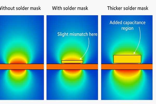
The most common solder mask material is Liquid Photoimageable (LPI). Its typical thickness is \(0.8-1.2 \text{ mils } (20-30 \text{ µm})\). However, the solder mask itself has a dielectric constant (\(\epsilon_{r}\) typically \(3.0-4.0\), varying by product). If the mask encroaches too closely on an RF trace or is too thick over it, it can slightly alter the trace's effective dielectric constant, shifting its impedance and increasing loss. This is particularly true at higher frequencies (\(>20 \text{ GHz}\)), where the interaction with the solder mask and underlying copper surface roughness becomes more pronounced. I always specify Non-Solder Mask Defined (NSMD) pads for critical RF components because they provide more consistent pad capacitance and better solder joint reliability. Crucially, I define the solder mask relief or "pullback" around RF pads and transmission lines—often \(75 \text{ µm}\) to \(100 \text{ µm } (3-4 \text{ mils})\) clearance from the copper edge.
Silkscreen: Keeping it Clear and Non-Interfering
For silkscreen, the primary rules are to ensure its material is non-conductive and to establish clear clearance rules. I specify that no silkscreen should be printed over exposed pads or any RF signal traces. A minimum clearance of \(0.05 \text{ mm } (2 \text{ mils})\) from such features is a good starting point. I also specify minimum line width (e.g., \(0.1 \text{ mm / } 4 \text{ mils}\)) for legibility.
Table: Solder Mask & Silkscreen Guidelines for RF
| Parameter | RF Consideration | Recommendation |
|---|---|---|
| Solder Mask | ||
| Material Type | Dielectric properties, adhesion | LPI (e.g., Taiyo PSR-4000 series or equivalent) |
| Thickness | Dielectric loading, planarity | Typically \(20-30 \text{ µm}\); specify if thinner/thicker needed |
| \(\epsilon_{r}\) of Mask | Impact on impedance/loss | Be aware (typically \(3-4\)); ensure adequate clearance |
| Openings for RF Pads | Minimize dielectric effect, accurate component placement | NSMD preferred; specify pullback (e.g., \(75-100 \text{ µm}\) from copper) |
| Openings for RF Traces | Minimize dielectric effect, impedance control | Define "keep-out" or specify minimum distance mask should be from trace edge |
| Silkscreen | ||
| Material Type | Non-conductive, no interference | Standard epoxy-based inks |
| Clearance from Pads/Traces | Avoid shorting, capacitive loading | Min. \(0.05 \text{ mm}\) from exposed copper; No silkscreen over RF traces |
| Min. Feature Size | Legibility | E.g., \(0.1 \text{ mm}\) line width, \(0.8 \text{ mm}\) character height |
Why Explicitly List PCB Material Choices For RF Board Fabrication?
Have RF designs failed due to unexpected material substitutions from the fab house? I've learned that assuming your fab house knows the "best" RF material for your specific application is a risky bet. Explicitly listing your material choices is crucial for performance.
Explicitly list PCB material choices for RF boards because properties like dielectric constant (\(\epsilon_{r}\)), loss tangent (\(\tan\delta\)), their stability over frequency and temperature, and copper surface roughness directly impact impedance, signal loss, and overall RF performance. Generic FR-4 is often unsuitable.
Material selection is absolutely fundamental in RF PCB design. You cannot afford ambiguity here.
Core Dielectric Properties and Their RF Impact
I always specify the exact manufacturer and material grade (e.g., Rogers RO4350B, not just "a Rogers material"). This is because even within a manufacturer's families, different grades can have variations. The dielectric constant (\(\epsilon_{r}\)) and loss tangent (\(\tan\delta\))6 are the headliners. For instance, RO4350B's \(\epsilon_{r}\) is \(3.48 \pm 0.05\) and \(\tan\delta\) is \(0.0037\) (both at \(10 \text{ GHz, } 23^\circ\text{C}\), per Rogers Corp. datasheet). These values vary with frequency, temperature (defined by TCEr – Thermal Coefficient of Dielectric Constant), and even moisture absorption. For high-performance RF, you need materials where these parameters are stable and well-characterized across your operating conditions.
Copper Foil: Not All Copper is Created Equal for RF
The type and properties of the copper foil are critical. Copper surface roughness7 (often given as \(R_{z}\) or \(R_{q}\)) plays a huge role in conductor losses at high frequencies, especially above a few GHz and becoming dominant over \(20 \text{ GHz}\). The skin effect forces current to flow near the surface. A rougher surface increases the effective path length for the current, thus increasing losses. Standard ED copper might have an \(R_{q}\) of \(1.5-3 \text{ µm}\). For RF, smoother foils like VLP (Very Low Profile, \(R_{q} \approx 0.8-1.2 \text{ µm}\)) or HVLP (Hyper Very Low Profile, \(R_{q} \approx 0.3-0.5 \text{ µm}\)) are often specified. I ensure this is clear in the stack-up.
Table: Key RF Material Parameters and their Significance
| Parameter | Typical Value Range for RF (example) | RF Impact |
|---|---|---|
| Dielectric Constant (\(\epsilon_{r}\)) | \(2.0 - 10.0\) | Affects impedance, signal velocity, physical size of structures |
| Loss Tangent (\(\tan\delta\)) | \(0.001 - 0.025\) | Determines dielectric losses (signal attenuation) |
| Thickness Tolerance | \(\pm 5\%\) to \(\pm 10\%\) (per IPC-4101) | Critical for impedance control |
| TCEr (\(\text{ppm}/^\circ\text{C}\)) | \(< 50 \text{ ppm}/^\circ\text{C}\) | Stability of \(\epsilon_{r}\) over temperature |
| Copper Roughness (\(R_{q}\)) | \(0.3 \text{ µm}\) (smooth) - \(3.0 \text{ µm}\) (standard ED) | Affects conductor loss (skin effect), phase delay at high frequencies |
| Moisture Absorption | \(< 0.2\%\) | Can alter \(\epsilon_{r}\) and \(\tan\delta\) |
Stating "No substitutions" or providing a very short, pre-approved list of alternatives is my standard practice.
When Should Via Plugging Or Filling Be Specified For RF PCBs?
Are vias causing you RF headaches? I know that open or improperly treated vias can lead to solder wicking, shorts during assembly, or inconsistent grounding. Specifying via treatment is important for robust RF designs.
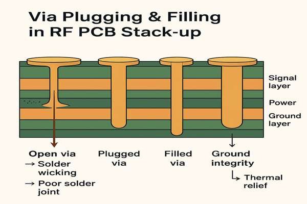
Via plugging or filling should be specified for RF PCBs when vias are located in pads (via-in-pad designs), especially under BGA or QFN components to prevent solder wicking and ensure good solder joints, or when a flat, continuous surface is needed for component mounting or thermal management.
Via treatments are crucial for assembly yield and sometimes for RF performance, especially with dense designs.
Understanding Via Treatments
The IPC-4761 standard defines various via protection types. Common ones I encounter are:
- Type III-a/b (Tented/Covered): Solder mask covers the via hole. Cheapest, but can trap air/flux.
- Type IV-a/b (Plugged/Covered): Hole filled with non-conductive paste, then overprinted by solder mask. Better seal.
- Type VI (Filled/Covered): Hole filled (often conductive/non-conductive epoxy), planarized, then solder mask covered.
- Type VII (Filled/Capped): Hole filled, planarized, then plated over with copper. Most robust for via-in-pad.
RF Implications of Via Treatments
For Via-in-Pad (VIP) designs, common under BGAs or QFN thermal pads, filling and capping (IPC-4761 Type VII8) is often essential. This prevents solder wicking down the via during reflow, ensuring a good solder joint and a planar surface. Conductive fill (e.g., silver epoxy like Dupont CB100 or Tatsuta AGP Series) can offer improved thermal conductivity for thermal vias under power devices. It may also slightly reduce via inductance for critical RF ground connections, but usually, an array of well-placed standard (non-filled) vias or non-conductively filled vias provides adequate RF grounding. The cost of conductive fill is significantly higher. For most signal vias, non-conductive fill or simple plugging is sufficient unless they are in a pad.
Table: Comparison of Common Via Treatments
| IPC-4761 Type | Description | RF Benefit/Consideration | Typical Use Case |
|---|---|---|---|
| Type III-a | Tented (one side) | Minimal cost; potential for flux entrapment. | Non-critical vias away from pads. |
| Type IV-a | Plugged (non-conductive paste) | Prevents solder wicking; better seal than tenting. | Vias near SMT pads, but not in-pad. |
| Type VII | Filled (epoxy) & Capped (plated) | Best for VIP; planar surface; good thermal path if conductive fill. | Via-in-Pad, thermal vias. |
I always specify the IPC type needed, and if filled, the fill material (conductive or non-conductive).
What PCB Surface Finish Is Often Preferred For RF Signal Integrity?
Experiencing unexpected signal loss or intermodulation in your RF circuits? Your PCB surface finish might be the culprit. I've learned that choosing the right finish is key for maintaining high-frequency performance and signal integrity.
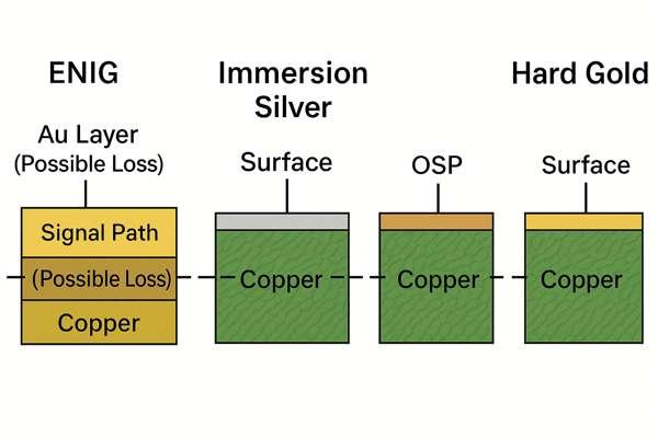
Electroless Nickel Immersion Gold (ENIG) is often preferred for RF signal integrity due to its flat surface, good solderability, and relatively minimal impact on high-frequency losses for many applications. For very high frequencies or extreme PIM sensitivity, alternatives like Immersion Silver or direct gold plating might be considered.
The surface finish affects solderability, reliability, and critically, RF performance.
Key Characteristics of RF-Friendly Finishes
For RF, I look for finishes that offer:
- Planarity (Flatness): Essential for consistent solder joints with fine-pitch SMT components and for predictable launches of RF signals onto transmission lines.
- Low Signal Loss: The finish materials and their thickness can influence conductor losses, especially at higher frequencies due to the skin effect.
- Good Solderability & Reliability: Must form strong, reliable solder joints.
- Minimal PIM (Passive Intermodulation)9: Important for communications infrastructure.
Comparing Common Finishes for RF Applications
ENIG (Electroless Nickel Immersion Gold) is a popular choice. The gold layer (\(0.05-0.1 \text{ µm / } 2-4 \text{ µin}\)) protects the solderable nickel layer (\(3-6 \text{ µm / } 120-240 \text{ µin}\)). It's very flat. A concern for some ultra-sensitive applications is that nickel is ferromagnetic and can introduce minute PIM or losses; however, for most RF work up to \(20-30 \text{ GHz}\), it performs well.
Immersion Silver (ImAg) offers excellent conductivity and a very flat surface, leading to lower loss than ENIG at very high frequencies. However, it can tarnish and has a shorter shelf life.
ENEPIG (Electroless Nickel Electroless Palladium Immersion Gold) adds a palladium layer, improving wire bondability and mitigating some ENIG concerns like "black pad" (though modern ENIG processes have largely addressed this). It's more expensive.
HASL is generally not suitable for RF due to its uneven surface.
Table: Surface Finish Comparison for RF (Simplified)
| Finish | Key Pros for RF | Key Cons for RF | Typical RF Use | Roughness Impact Note |
|---|---|---|---|---|
| ENIG | Flat, good solderability, good shelf life | Nickel properties (PIM/loss at V. High Freq.) | General RF up to \(\approx 30 \text{ GHz}\) | Underlying copper roughness still dominant |
| ImAg | Very flat, excellent conductivity, lower loss | Tarnishes, shorter shelf life, micro-voids possible | High Freq. (\(>20 \text{ GHz}\)), low PIM apps | Underlying copper roughness still dominant |
| ENEPIG | ENIG benefits + wire bondable, better PIM | Higher cost | Mixed signal, high reliability | Underlying copper roughness still dominant |
| Direct Gold | Excellent for RF, bondable | Very expensive, often specialized process | Microwave/mmWave, critical apps | Can be very smooth |
Crucially, the surface roughness of the copper beneath the finish still significantly impacts losses at high frequencies. A smooth underlying copper is beneficial regardless of the finish chosen.
How Do RF PCB Panelization Notes Differ From Standard Boards?
Facing issues when depaneling your delicate RF boards, or seeing performance variations near the edges? Standard panelization might not suit sensitive RF circuits or brittle RF materials. Specific notes can prevent damage and ensure consistency.
RF PCB panelization notes should emphasize minimizing stress during depaneling (e.g., using tab-routing with mouse bites over deep V-grooves for sensitive substrates) and maintaining impedance consistency and ground continuity near panel edges or where coupons are placed.
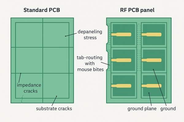
Panelization strategies need careful thought for RF boards, especially those using brittle or soft RF laminates.
Minimizing Stress on RF Substrates
Many RF substrates (e.g., ceramic-filled PTFE like Rogers RO3000 series, or actual ceramic substrates) are more prone to stress fractures or delamination than standard FR-4.
- V-Groove (Scoring): While efficient, V-grooves can impart significant stress. If used, I specify a shallow V-groove (e.g., remaining web \(\approx \frac{1}{3}\) of board thickness) and ensure it's far from critical RF traces or components.
- Tab-Routing10 (with "Mouse Bites"): This is often preferred for RF boards. It involves leaving small tabs connecting the board to the panel, which are later broken or cut. The "mouse bites" (a series of small holes) in the tabs create defined break points. This generally induces less stress. I specify tab width, number/size of holes, and their placement away from sensitive areas.
Table: Panelization Methods for RF PCBs
| Method | Description | Pros for RF | Cons for RF | Best Suited For |
|---|---|---|---|---|
| V-Groove | Continuous V-shaped cut along board edges | Fast depaneling, clean edges (if done well) | High stress, risk of cracking brittle materials | Robust FR-4 based RF boards |
| Tab-Routing | Boards connected by small tabs with breakaway features | Lower stress, better for irregular shapes | Slower depaneling, may leave rougher "nubs" | Delicate/brittle RF substrates |
| Punching/Dicing | Specialized methods | Very clean edges, low stress (dicing) | Higher cost, specialized equipment needed | High volume, very sensitive boards |
Maintaining Electrical Integrity in Panel Form
If there are impedance test coupons or traces running near the edge of the individual PCB, the panel frame and its grounding can influence them. I ensure the panel design maintains ground plane continuity for such test structures. Strategic placement of test coupons to be representative of the board's actual conditions is also a note I include. Any areas with overhanging RF connectors need clear keep-outs from panelization features.
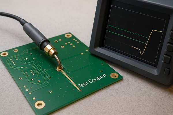
What Specific RF PCB Test (e.g., TDR) Can Be Requested From A Fab House?
Unsure if your fabricated RF boards meet critical impedance specifications? Don't just hope for the best; specific tests can verify performance. I always request the right tests to get that crucial validation.
Specific RF PCB tests like Time Domain Reflectometry (TDR) for controlled impedance verification can, and should, be requested from the fab house. They can provide test coupons and reports confirming that critical trace impedances are within specified tolerances (e.g., \(50 \Omega \pm 5\%\)).
Verification is key to confidence in RF PCB performance.
Impedance Verification: The Standard Request
Time Domain Reflectometry (TDR) is the industry standard for verifying controlled impedance.
- TDR Coupon Design: I ensure the test coupons on the panel have structures (trace width, dielectric spacing, reference planes) that closely mimic the actual controlled impedance lines on the board. The launch onto the coupon trace should also be representative. Coupon length should be sufficient for an accurate reading (typically at least \(15 \text{ cm / } 6 \text{ inches}\) if space allows, though shorter is common).
- Interpreting TDR Reports: I look for the report to show not just a pass/fail, but the measured impedance plot, average value, and min/max values over the trace length. This confirms it's within my specified tolerance (e.g., \(50 \Omega \pm 5\%\)).
Advanced RF Testing and Verification
While TDR is common from fab houses, other tests are usually performed by the design engineer or a specialized test lab:
- S-Parameter Measurements (VNA)11: Using a Vector Network Analyzer to characterize insertion loss, return loss, and coupling of specific structures or full channels. This is more comprehensive than TDR.
- Material Parameter Verification: For very critical designs or during R&D, one might need to verify the \(\epsilon_{r}\) and \(\tan\delta\) of the supplied materials. Methods like those described in ASTM D3380 ("Standard Test Method for Permittivity (Dielectric Constant) and Dissipation Factor of Electrical Insulating Materials at Power, Audio, and Radio Frequencies Including Microwave Frequencies") or using resonant techniques (e.g., split-post dielectric resonator) can be employed.
Table: RF PCB Test Methods
| Test | Purpose | When to Request/Perform | Typical Output |
|---|---|---|---|
| TDR | Verify Characteristic Impedance | Standard from Fab House for controlled \(Z\) lines | Impedance value (\(\Omega\)) vs. distance, Pass/Fail |
| 4-Wire Kelvin Resistance (Ohms) | Verify low resistance for critical power/ground paths | Request from Fab House or perform in-house | Resistance value (\(\text{m}\Omega\)) |
| S-Parameter Measurement (VNA) | Characterize Insertion Loss, Return Loss, Isolation etc. | Post-fabrication by designer/test lab | \(S_{11}\), \(S_{21}\), \(S_{12}\), \(S_{22}\) plots/data |
| Dielectric Material Testing | Verify \(\epsilon_{r}\), \(\tan\delta\) of raw materials | R&D, qualification, troubleshooting | \(\epsilon_{r}\), \(\tan\delta\) values at specific frequencies |
| AOI (Automated Optical Inspection) | Detect shorts, opens, feature size violations | Standard Fab House process | Defect report |
| AXI (Automated X-ray Inspection) | Inspect BGA solder joints, internal layer registration | Fab House (for BGAs) / Assembly House | X-ray images, defect report |
Standard process controls like AOI for shorts/opens and AXI for BGA integrity are also vital for overall RF board quality.
Conclusion
In my experience, providing comprehensive, precise information—from complete design files and detailed stack-ups to specific material choices, surface finish, and testing requirements—is absolutely paramount for successful RF PCB fabrication, ensuring on-spec performance and minimizing costly delays.
-
Understanding Gerber files is crucial for anyone involved in PCB design, as they are essential for manufacturing processes. ↩
-
A well-structured BOM is vital for sourcing and assembling RF components accurately, ensuring project success. ↩
-
Understanding the dielectric constant is crucial for optimizing RF performance and minimizing signal loss. Explore this link for in-depth insights. ↩
-
IPC-6012 Class 2 standards are essential for quality assurance in PCB manufacturing. Learn more about these specifications to enhance your projects. ↩
-
Time Domain Reflectometry is a critical technique for verifying impedance in PCBs. Learn more about its applications and benefits. ↩
-
The loss tangent is vital for assessing dielectric losses in RF materials. Discover its importance and how it influences signal quality. ↩
-
Copper surface roughness significantly impacts conductor losses in RF applications. Learn more about its effects and how to choose the right type. ↩
-
This link will help you grasp the significance of IPC-4761 Type VII, essential for robust via-in-pad designs in modern electronics. ↩
-
Learning about minimal PIM can improve communication quality and reduce interference in RF systems. ↩
-
Tab-Routing is a preferred method for RF boards, reducing stress and improving design flexibility. Learn more about its advantages here. ↩
-
Learn about S-Parameter Measurements to enhance your RF testing methods and ensure better signal integrity. ↩


