 Skip to content
Worried about hidden flaws in your new PCB assembly? These small electrical defects can cause major project delays. Flying probe testing finds these faults early, ensuring your board works correctly.
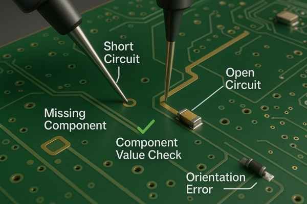
A flying probe test detects electrical defects like shorts, opens, and missing components. It also verifies component values (resistors, capacitors), and checks the orientation of parts like diodes and transistors by measuring electrical properties directly on the board without custom fixtures.
As a hardware engineer, I've seen countless projects saved by catching a simple short or a reversed diode before it became a major headache. Early testing isn't just a quality check; it's a critical step that saves time, money, and frustration. Flying probe testing is one of the most powerful tools in our arsenal, especially during the prototyping phase when designs are still changing. It gives us the confidence to move forward, knowing the basic electrical integrity of our assembly is solid. Let's explore what this test is and what it can do for your project.
What Is Flying Probe Testing in PCB assembly?
Struggling to justify expensive test fixtures for your prototypes? The costs can be prohibitive for small runs. Flying probe testing provides a fixtureless alternative, making thorough electrical testing affordable.
Flying probe testing is an automated electrical test method for Printed Circuit Board Assemblies (PCBAs). It uses multiple, independently moving probes to make contact with pads, vias, and component leads to check for manufacturing defects like shorts, opens, and incorrect component placement.
Flying probe testing, often abbreviated as FPT, is defined by its core principle: it is a non-contact, fixtureless method. The name "flying probe" comes from the way the test probes rapidly move—or "fly"—from point to point across the board. Unlike traditional In-Circuit Testing (ICT), which requires a custom "bed-of-nails" fixture for every unique PCB design, FPT relies entirely on software. This completely eliminates the cost and lead time associated with designing, manufacturing, and debugging a physical fixture.
When is Flying Probe Testing the Best Choice?
This software-driven approach makes FPT the perfect choice for several common engineering scenarios:
| Scenario | Why FPT is Ideal | My Experience |
|---|---|---|
| Prototyping & NPI | Design changes are frequent. FPT's software-based setup can be updated in hours without any hardware cost, unlike a rigid fixture. | For new product introductions (NPI), we would often have 3-4 board revisions. FPT allowed us to test each one without incurring new tooling costs. |
| Low to Medium Volume | The high cost of an ICT fixture (often >$10,000) cannot be justified by a small production run. FPT has virtually no setup cost. | For a medical device project with an annual volume of 500 units, FPT was the only economically viable electrical test solution. |
| High-Mix Manufacturing | A manufacturer producing dozens of different board designs each month would go bankrupt on fixture costs. FPT can switch between jobs instantly. | I've worked with contract manufacturers who run 20 different customer boards on the same FPT machine in a single day. |
How Does a Flying Probe Tester Work?
Ever wonder how a machine can test a complex board without any custom tooling? The process seems complex. But it's a straightforward system combining robotics and electrical measurement.
A flying probe tester uses 4 to 8 independently controlled probes that move to specific coordinates on the PCB based on CAD data. The probes make contact with component leads or test pads to perform electrical measurements, such as resistance, capacitance, and voltage, to detect faults.
The entire process is driven by software and precision mechanics. It can be broken down into three main stages. First, a test program is generated from the board's design files. Second, the machine's robotic probes move across the board according to the program. Finally, the probes perform a series of specific electrical measurements.
What Electrical Measurements a Flying Probe Tester Performs
The core of the test happens when the probes make contact. They perform thousands of individual measurements using very low voltages (typically under 200mV) to avoid turning on semiconductors.
| Measurement Type | Purpose | Typical Threshold / Technique |
|---|---|---|
| Continuity Test1 | To detect open circuits within a single net. | Measures resistance between two points. Fails if > 10 Ω. |
| Shorts Test | To detect shorts between two different nets. | Measures resistance between nets. Fails if < 100 kΩ. |
| Component Test | To verify the correct value of passive components. | Measures resistance, capacitance, or inductance. Compares to BOM. |
| Diode Test | To check the orientation of diodes and transistors. | Measures forward voltage drop (e.g., 0.5V - 0.8V). |
What Are the Main Advantages of Flying Probe Testing?
Need to test your prototypes quickly without breaking the bank? The high upfront cost of traditional testing can be a major barrier. Flying probe testing offers a cost-effective and flexible solution.
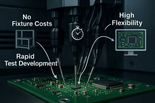
The main advantages of flying probe testing are its lack of fixture costs, rapid test program development, and high flexibility for design changes. This makes it ideal for prototyping, low-volume production, and high-mix manufacturing environments where speed to market is critical.
Key Advantages of FPT Over Fixture-Based Testing
In my career, especially during new product introduction (NPI), flying probe testing has been invaluable. The advantages become crystal clear when you compare it to fixture-based methods like ICT.
| Advantage | Description | My Experience |
|---|---|---|
| No Fixture Costs | FPT is a fixtureless system. This eliminates the need to design, build, and maintain expensive "bed-of-nails" fixtures, which can cost anywhere from $5,000 to $50,000 or more. | On the Tuxedo Keypad project, we had multiple board variants. Using FPT for early builds saved us a significant portion of the tooling budget. |
| Fast Turnaround | Test programs are generated directly from CAD data. Setup can be completed in hours, whereas designing and fabricating an ICT fixture can take several weeks. | I've been able to get test results from a new board layout the day after it comes out of the reflow oven. This speed is crucial for tight development schedules. |
| High Flexibility | If the board design changes, you only need to update the software program. With ICT, a board revision often requires a costly and time-consuming fixture modification. | When we had to swap a component due to supply chain issues, updating the FPT program was a simple software change that took less than an hour. |
| Precise Fault Location | FPT provides the exact X-Y coordinates of failures. This precision dramatically speeds up the rework and debugging process. | This is much better than a functional test that just reports "FAIL." The repair technicians can go directly to the source of the problem. |
What Are the Limitations of Flying Probe Testing?
Is flying probe testing the right choice for every situation? While it's great for prototypes, its speed can become a bottleneck. It's important to understand where it falls short.
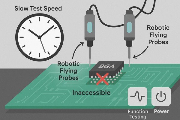
The primary limitations of flying probe testing are its slower test speed compared to ICT, making it less suitable for high-volume production. It also has limited ability to test components under BGA packages and cannot perform functional or power-on testing.
Understanding the Limitations of Flying Probe Testing
While I rely heavily on FPT for new designs, I'm also keenly aware of its limitations. Choosing the right test strategy means acknowledging the trade-offs.
| Limitation | Description | Impact on Projects |
|---|---|---|
| Slower Test Speed | FPT tests points sequentially. A typical board can take 30 to 90 seconds to test, whereas ICT tests all points in parallel in about 5 to 10 seconds. | For high-volume manufacturing, this slow speed creates a bottleneck. Once a product ramped up to mass production, we always transitioned to ICT. |
| Limited Access to BGAs | Probes need physical access to an electrical node. They cannot test connections directly under a Ball Grid Array (BGA) or other leadless packages. | To test BGAs, FPT must be combined with other methods like Boundary Scan (JTAG) or X-ray inspection to ensure all solder balls are properly connected. |
| No Dynamic/Functional Testing | FPT is a passive, unpowered test. It cannot verify timing-critical circuits (like a high-speed memory interface) or the dynamic interaction between components under real operating conditions. | It can tell you a resistor is the correct value, but it can't tell you if the CPU will boot or if the power supply is stable under load. Functional testing is a separate, necessary step. |
| Cannot Test Press-Fit Connectors | Flying probes lack the high insertion force needed to make reliable contact with press-fit connector pins. These typically require a dedicated fixture with specialized probes. | For boards with many press-fit components, FPT coverage will be incomplete, and another test method is needed to verify those connections. |
What Is the Difference Between Flying Probe Testing and In-Circuit Testing (ICT)?
Choosing between FPT and ICT for your project? The decision depends heavily on your production volume and budget. They are both powerful tools, but they solve different problems.
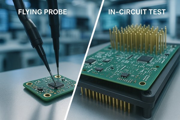
The main difference is that flying probe testing (FPT) is a fixtureless, sequential test ideal for low-volume and prototypes, while in-circuit testing (ICT) uses a custom "bed-of-nails" fixture for high-speed, parallel testing suited for mass production.
FPT vs. ICT: A Head-to-Head Comparison
I've managed projects that started with FPT for the initial prototypes and later transitioned to ICT as we scaled up. This table summarizes the key trade-offs.
| Feature | Flying Probe Testing (FPT) | In-Circuit Testing (ICT) |
|---|---|---|
| Test Fixture | None (Fixtureless) | Custom "bed-of-nails" fixture required |
| Initial Cost | Very low. The main cost is programming time, typically a few hundred dollars. | Very high. Fixture design and fabrication can cost $5,000 to $50,000+. |
| Test Speed (per board) | Slower. Typically 30-90 seconds. | Faster. Typically 5-10 seconds. |
| Ideal Production Volume | Prototypes and low-to-medium volume (1-1,000 units). | High volume (1,000+ units). |
| Fault Coverage | Excellent for manufacturing defects (shorts, opens, passives). Limited power-off test. | Can include basic powered checks (e.g., voltage rail verification) in addition to manufacturing defects. |
| Time to First Test | Fast. Test programs can be ready in a few hours. | Slow. Fixture development can take 2-4 weeks. |
When Is Flying Probe Testing Preferable to Automated Optical Inspection (AOI)?
Confused about whether to use FPT or AOI? They sound similar but look for completely different types of defects. One uses electricity, the other uses cameras.
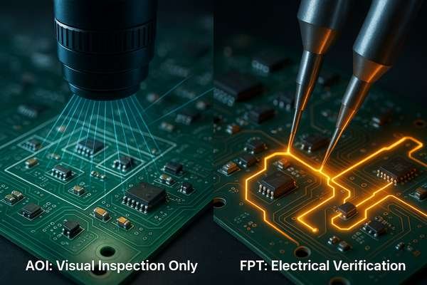
Flying probe testing (FPT) is preferable to automated optical inspection (AOI) when you need to verify electrical characteristics, not just visual appearance. FPT finds shorts, opens, and incorrect component values, which AOI cannot detect.
On my projects, we never choose between FPT and AOI. We use both. They are complementary technologies that provide much higher test coverage when combined.
Electrical Verification (FPT) vs. Visual Inspection (AOI)
Think of it this way: AOI checks if the board looks right, while FPT checks if it works right electrically. Modern 3D AOI systems are excellent at spotting visual defects but are blind to electrical properties.
| Test Focus | Flying Probe Testing (FPT) | Automated Optical Inspection (AOI) |
|---|---|---|
| Primary Goal | Verify electrical integrity and component values. | Verify visual correctness of assembly. |
| Finds This | Shorts, opens, incorrect R/L/C values, reversed diodes. | Missing parts, wrong polarity markings, solder bridges, poor solder joints. |
| Misses This | Solder joint quality, cosmetic defects, polarity markings. | Incorrect electrical values, shorts under BGAs, open circuits. |
How FPT and AOI Work Together in Production
A typical high-reliability production line uses them in sequence: AOI runs right after soldering to catch assembly process errors, and FPT runs after that to catch the electrical faults that AOI missed. This ensures both visual and electrical quality are verified.
Can Flying Probe Testing Detect Incorrect Component Values?
Worried that the wrong resistor or capacitor was placed on your board during assembly? Such a mix-up can be very difficult to debug later. Flying probe testing can catch these issues early.
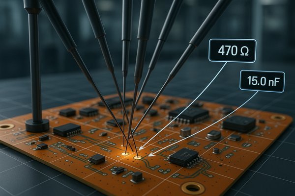
Yes, flying probe testing can accurately detect incorrect component values. The tester's probes measure the resistance, capacitance, and inductance of passive components on the board and compare the results to the expected values from the Bill of Materials (BOM).
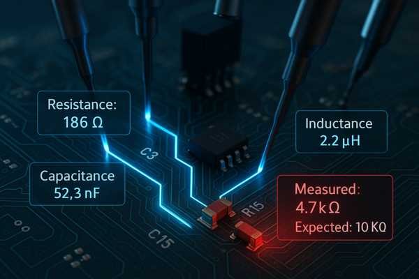
Measuring Passive Components with High Accuracy
This is one of the most powerful features of FPT. It can measure components with high precision.
| Component Type | Measurement Method | Typical Accuracy |
|---|---|---|
| Resistor | 4-Wire (Kelvin) Measurement2 | ±1% to 5% |
| Capacitor | AC Impedance Measurement | ±5% to 10% |
| Inductor | AC Impedance Measurement | ±5% to 10% |
How "Guarding" Isolates Components for Accurate Testing
When a component is in parallel with others, the measurement can be skewed. To solve this, testers use guarding. This technique uses extra probes to apply voltages that electrically isolate the component under test, allowing for an accurate measurement even in a complex network.
Can Flying Probe Testing Check the Orientation of Diodes and Transistors?
Afraid a reversed diode or transistor might damage your circuit when you power it on for the first time? This is a common assembly error. Flying probe testing provides an effective way to check.
Yes, flying probe testing can reliably check the orientation of diodes and transistors. It does this by performing diode-junction tests, measuring the forward voltage drop across the semiconductor junctions to confirm they are correctly oriented in the circuit.
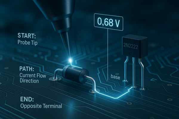
Verifying Semiconductor Orientation with FPT
Catching orientation errors before power-up is a huge time-saver. FPT automates this check for various components.
| Component | Test Method | What It Verifies |
|---|---|---|
| Standard Diode | Forward/Reverse Bias Test | Orientation, presence, and shorts/opens. |
| Zener Diode | Reverse Breakdown Test | Correct Zener voltage (e.g., 5.1V) and orientation. |
| BJT Transistor | Diode Junction Test | Orientation of Base-Emitter and Base-Collector junctions. |
| MOSFET | Body Diode Test | Presence and orientation of the intrinsic body diode. |
How Are Shorts and Opens Detected Using a Flying Probe Tester?
Are you concerned about tiny, invisible shorts or broken traces on your freshly assembled boards? These are among the most common manufacturing defects. Flying probe testing is specifically designed to find them.
Shorts are detected by checking for low resistance between two separate electrical nets. Opens are detected by checking for high resistance between two points on the same net. The tester uses the board's netlist from CAD data as the source of truth.
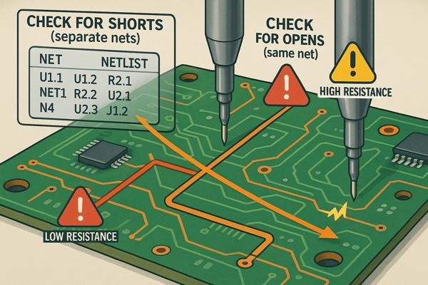
The Fundamental Tests for Finding Shorts and Opens
This capability is what makes FPT so essential.
| Defect Type | Test Principle | Resistance Threshold (Typical) |
|---|---|---|
| Open Circuit | Measures resistance between two points on the same net. A high resistance indicates a break. | > 10 Ω (Flags as an Open) |
| Short Circuit | Measures resistance between two points on different nets. A low resistance indicates a bridge. | < 100 kΩ (Flags as a Short) |
Modern FPT software optimizes the shorts test by using PCB layout data to intelligently test only between nets that are physically close, making the process much more efficient.
What are the design for testability (DFT) guidelines for flying probe testing?
Want to make testing your boards easier and more reliable? While FPT is flexible, following a few simple design rules can significantly improve test coverage and speed.
Key Design for Testability (DFT) guidelines for flying probe testing include providing adequate clearance around test points, using sufficiently large test pads, avoiding tall components near test areas, and providing complete and accurate CAD and BOM data to the test house.
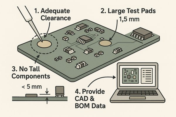
Key DFT Guidelines for Reliable Flying Probe Testing
As an engineer, I always think about testing during the design phase. A little planning goes a long way.
| Guideline | Specification / Rule of Thumb | Reason |
|---|---|---|
| Test Pad Size | ≥ 0.8 mm (31.5 mils) diameter. 1.0 mm is ideal. | Provides a large, stable target for the probe, reducing contact errors and false failures. |
| Pad Clearance | ≥ 0.5 mm (20 mils) from pad edge to component body. | Prevents the probe from accidentally hitting an adjacent component during contact. |
| Component Height | Keep tall components (> 10 mm) away from test areas. | Tall components can physically block the probe's access path to nearby test points. |
| Via Tenting | Leave vias intended for testing un-tented (exposed). | Solder mask is an insulator. A probe cannot make electrical contact through it. |
| Data Integrity | Provide complete and accurate CAD, BOM, and Centroid files. | The test program is generated from this data. Garbage in, garbage out. |
Conclusion
Flying probe testing is a flexible, fixtureless method for finding electrical faults in PCBAs. It is an essential tool for prototypes and low-volume production, ensuring your hardware works as designed.


