 Skip to content
Struggling with clock distribution? Multiple devices need the same clock, but one source can't drive them all without degrading the signal. This causes system-wide timing chaos.
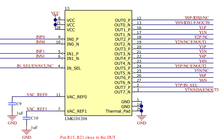
A typical clock buffer schematic shows a clock input pin, power/ground pins, control pins like enable/disable, and multiple fan-out output pins. The core component is an IC, like a Texas Instruments LMK1D1208, that takes one clock signal and cleanly replicates it to several loads.
A schematic is just the beginning. The real engineering work is in the implementation, which is what separates a stable system from an unreliable one that gives you headaches for weeks. How you power the buffer, where you place it, and how you route the signals are far more important than just connecting the dots on a schematic. Let's dive into the details that truly matter for a robust design, starting with the power supply.
What is the correct way to power a clock buffer to minimize noise?
Is power supply noise coupling into your clock buffer? This jitter can destroy your system's timing margins, leading to intermittent and incredibly hard-to-debug failures in the field.
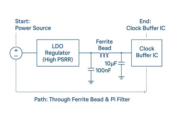
To power a clock buffer correctly, use a dedicated low-noise LDO with a high Power Supply Rejection Ratio (\(PSRR\)). Place decoupling capacitors (e.g., \(100\text{nF}\) and \(1-10\mu\text{F}\)) right at the IC’s power pins and use a ferrite bead on the power input to form a Pi filter.
In my experience, the power delivery network for clocking circuits is one of the first places I scrutinize. A noisy power rail directly translates to clock jitter1. A clean power delivery network is non-negotiable, and I focus on three key areas to achieve it.
Choosing the Right LDO
Not all LDOs are created equal. For clocking circuits, I look for an LDO with a very high Power Supply Rejection Ratio2 (\(PSRR\)). \(PSRR\) measures the LDO's ability to block noise from its input. You need to check the \(PSRR\) value in the datasheet at the frequencies that matter most—typically the switching frequency of any upstream SMPS3 (e.g., \(100 \text{ kHz}\) to \(2 \text{ MHz}\)). A good choice will have a \(PSRR\) of \(>60 \text{ dB}\) in this range, ensuring that noise from the main power supply doesn't get through to your sensitive clock buffer.
The Pi Filter: Decoupling and Filtering
The ferrite bead and capacitors form a crucial Pi filter right at the IC. This local network provides clean power and is your first line of defense.
| Component | Typical Specification/Value | Primary Function |
|---|---|---|
| Low-Noise LDO | \(PSRR > 60 \text{ dB @ } 1 \text{ MHz}\) | Rejects noise from the main power rail. |
| High-Frequency Cap | \(0.1\mu\text{F}\) (\(100\text{nF}\)), X7R, 0402 | Shunts high-frequency noise to ground locally. |
| Bulk Decoupling Cap | \(1\mu\text{F} - 10\mu\text{F}\), X5R, 0603 | Provides a local charge reservoir for the IC. |
| Ferrite Bead | \(>100\Omega \text{ @ } 100\text{MHz}\) | Filters high-frequency noise from the power trace. |
Grounding for Maximum Isolation
How you connect to ground is critical. All ground pins on the buffer and its decoupling capacitors should have a direct, low-inductance path to the ground plane using multiple vias. For maximum isolation, I often create a "quiet island" — a small, dedicated ground polygon for the clock buffer circuit. This island is then connected to the main system ground at a single point, preventing noisy return currents from other parts of the board from flowing under the clock buffer and corrupting its reference.
Where should a clock buffer be placed on a PCB for optimal performance?
Did you place your clock buffer in a convenient but technically wrong spot? Now you're dealing with long, meandering clock traces, causing significant timing skew and signal integrity nightmares across your board.
For optimal performance, place the clock buffer physically central to all the devices it drives. This floorplanning strategy allows for shorter, direct, and equal-length traces, which is the key to minimizing timing skew and preserving signal integrity.
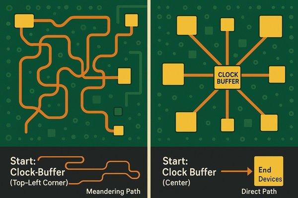
I think of clock buffer placement as a strategic decision made during the board's initial floorplanning. The goal is a star distribution where the buffer is the center. This isn't just a recommendation; it's a fundamental principle for high-speed design.
Strategic Floorplanning and Skew
Electricity travels through a PCB trace at roughly \(15 \text{ cm per nanosecond}\). If one clock trace is just \(2 \text{ cm}\) longer than another, that's a skew of about \(133 \text{ ps}\). For an interface like DDR4 memory where the total skew budget between clock and data can be as tight as \(\pm25 \text{ ps}\), that \(133 \text{ ps}\) is an instant failure. This is why proper floorplanning isn't optional. Placing the buffer centrally makes it physically possible for the layout engineer to route traces of nearly identical lengths.
The Importance of the Input Trace
While the buffer should be central to its loads, the trace from the primary clock source (like a crystal oscillator) to the buffer's input pin is also critical. This input trace must be as short and direct as possible. Any noise or reflection on this single input will be amplified and distributed to all outputs. I treat this input trace with the same care as the outputs: controlled impedance and properly shielded.
Creating Quiet Zones
The buffer's location must be defensively chosen. I work with the layout team to partition the board into "noisy" zones (power supplies, motor drivers) and "quiet" zones (CPUs, memory, analog circuits). The clock buffer and its entire distribution network must reside firmly in a quiet zone.
| Placement Rule | Rationale | Implementation Tip |
|---|---|---|
| Central to Loads | Minimize trace length variance & total skew. | Place buffer physically equidistant from all driven ICs. |
| Close to Source | Preserve the integrity of the input signal. | Keep input trace \(< 2-3 \text{ cm}\). |
| Isolate from Noise | Prevent noise coupling into the clock circuit. | Maintain a \(>5 \text{ mm}\) keep-out from SMPS, relays, etc. |
What are the best practices for routing clock signals on a PCB?
Are your clock signals causing crosstalk or suffering from reflections? Poor routing practices are a common mistake that can turn a clean, stable clock from your oscillator into a noisy, unreliable source of system-wide failures.
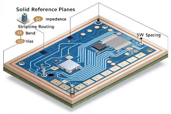
Route clock signals as \(50\Omega\) controlled-impedance traces on an inner layer (stripline), sandwiched between solid reference planes. Keep traces short, use gentle \(45^{\circ}\) bends, avoid vias, and maintain aggressive spacing (5W rule or more) to prevent crosstalk.
Routing a clock signal is not like routing a GPIO. It's a high-frequency analog signal. At Lightelligence, we traced a critical system instability back to a single clock trace that crossed a split in the ground plane. Fixing that one trace saved the entire project timeline.
Controlled Impedance4 and Shielding
To prevent reflections, the trace impedance must match the driver and receiver. The industry standard is \(50\Omega\). For shielding, I strongly prefer routing critical clocks on inner layers in a stripline configuration over an outer layer microstrip configuration. The two ground planes of a stripline provide excellent E-field containment.
Critical Routing Geometry
The physical path of the trace matters. I have hard rules for clock routing that I never violate.
| Routing Rule | Typical Value / Method | Reason |
|---|---|---|
| Controlled Impedance | \(50\Omega\) | Prevents signal reflections, ensures signal integrity. |
| Reference Plane | Solid, un-split Ground or Power plane | Provides a direct return path, minimizing loop area. |
| Bend Style | Two \(45^{\circ}\) bends or a curved arc | Avoids impedance discontinuities from sharp \(90^{\circ}\) corners. |
| Vias | Avoid if possible; use ground stitching vias if necessary | Avoids impedance bumps and signal stubs. |
| Spacing | >5W Rule (space = 5x trace width) | Prevents crosstalk from adjacent signals. |
Implementing Length Matching
To equalize delays between different clock branches, we add length to the shorter traces using serpentine "accordion" or "trombone" sections. These must be designed carefully: the segments within the accordion should be spaced widely (at least 3-4x the trace width) and be longer than the trace width to prevent them from coupling to each other and creating their own signal integrity problem.
How are clock buffer outputs terminated?
Are you seeing ugly ringing and overshoot on your clock lines? An unterminated or improperly terminated clock signal will reflect off the end of the trace, corrupting the signal integrity and causing false clock edges.
Clock buffer outputs are most commonly terminated with a series resistor (e.g., \(22-33\Omega\)) placed as close as possible to the buffer's output pin. The resistor's value is chosen so that its value plus the buffer's output impedance matches the trace's characteristic impedance (typically \(50\Omega\)).
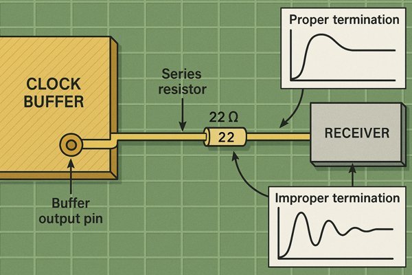
Termination is all about absorbing signal energy to prevent reflections. While simple rules of thumb work for non-critical signals, I rely on simulation for high-speed clocks.
Simulation-Driven Termination with IBIS
The most reliable way to determine the perfect termination value is to use IBIS (Input/Output Buffer Information Specification) models5. These are text files provided by the IC manufacturer that accurately describe the electrical behavior of the pins. I use a signal integrity simulator like HyperLynx, import the IBIS models for the driver and receiver, and simulate the real PCB trace. This process removes guesswork and lets me optimize for minimal overshoot and clean edges before the first prototype is ever built.
Practical Termination Schemes
Series termination is my go-to for point-to-point clocks. The resistor should be placed as close to the driver's pin as possible, ideally within \(50-100 \text{ mils}\) (\(1.27-2.54 \text{ mm}\)). For other topologies, different schemes are needed.
| Termination Type | Best For | Pros | Cons |
|---|---|---|---|
| Series | Point-to-point, single load | Low power, simple, effective | Not ideal for multi-drop topologies |
| Parallel (to GND) | Long traces, bused signals | Excellent signal quality at the end | Consumes DC power, adds a component |
| Thevenin Parallel | Bused signals (e.g., DDR memory) | Sets DC bias, great signal quality | High power consumption, two resistors |
| AC Termination | AC-coupled signals | No DC power consumption | Can distort duty cycle if not sized correctly |
How can the implementation of a clock buffer impact EMI/EMC performance?
Are you failing EMC testing because of radiated emissions from your clock harmonics? A poorly implemented clock buffer and its routing can act as a very efficient radio antenna, causing costly and time-consuming compliance failures.
A clock buffer impacts EMI by creating high-frequency current loops. Proper implementation—using series termination to slow signal edges, routing over a solid ground plane to minimize loop area, using Spread Spectrum Clocking (SSC), and shielding traces—dramatically reduces emissions.
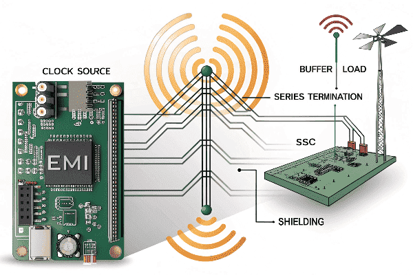
Passing EMC compliance is not luck; it's deliberate design. Clock circuits are often the #1 source of radiated emissions. Here's how I tackle the problem.
Fundamental Principles: Slew Rate6 and Loop Area
Two principles are paramount for controlling EMI:
- Slower Edges Radiate Less: The faster the rise/fall time, the more high-frequency harmonics it contains. A series termination resistor forms an RC low-pass filter with the trace capacitance, which gently slows the slew rate just enough to reduce the highest-frequency content without violating timing.
- Small Loops Radiate Less: EMI radiation is directly proportional to the area of the signal's current loop. By routing over a solid, uninterrupted ground plane, the return current stays directly under the trace, keeping the loop area microscopic and minimizing radiation.
An Advanced Technique: Spread-Spectrum Clocking (SSC)7
This is a powerful technique for EMI reduction. Many modern clock generators include an SSC feature. It works by intentionally modulating the clock frequency by a tiny amount (e.g., \(\pm0.5\%\)). This spreads the concentrated energy of a single frequency peak over a wider band.
| Technique | Primary Effect | Typical EMI Reduction |
|---|---|---|
| Series Termination | Increases rise/fall time (slows slew rate). | \(3-6 \text{ dB}\) |
| Minimize Loop Area | Reduces the radiation efficiency of the trace. | \(>20 \text{ dB}\) |
| Spread-Spectrum Clocking (SSC) | Spreads harmonic energy over a wider band. | \(8-12 \text{ dB}\) |
| Shielding (Stripline) | Contains electric fields around the trace. | \(>10 \text{ dB}\) |
How are clock signal integrity issues debugged on a board?
Your board is unstable, and you suspect the clock is the culprit. But probing a high-speed clock signal without affecting its behavior seems almost impossible, making the debugging process feel like a frustrating guessing game.
To debug clock signal integrity, use a high-bandwidth oscilloscope (\(>5\times\) the clock frequency) with a low-capacitance active probe (\(<1 \text{ pF}\)) connected to a dedicated test point. Analyze the eye diagram and use jitter decomposition tools to find the root cause.
You can't fix what you can't see. Having the right tools and knowing what to look for is everything.
Design for Test (DFT): Tools and Test Points
You need a scope with a bandwidth at least \(5\times\) the clock's frequency (e.g., a \(1 \text{ GHz}\) scope for a \(200 \text{ MHz}\) clock) and a low-capacitance (\(<1 \text{ pF}\)) active FET probe. Crucially, you must plan for this. During layout, I always add small, dedicated probing pads (\(20 \text{ mil}\) / \(0.5\text{mm}\)) for every critical clock line right at the receiver's pin. This makes debugging fast, safe, and accurate.
Interpreting the Waveform
When I'm looking at a clock signal on a scope, I'm hunting for these specific problems. The eye diagram is the best tool for visualizing these issues all at once.
| Observation (on Scope) | Appearance | Likely Cause(s) |
|---|---|---|
| Overshoot / Ringing | Signal exceeds \(V_{CC}\)/GND then oscillates. | Improper termination, impedance mismatch. |
| Slow Rise Time | Sloped edge instead of a sharp vertical line. | Excessive capacitance, weak driver. |
| Jitter | Horizontal "fuzziness" of edges in an eye diagram. | Reflections, crosstalk, noisy power supply. |
| Non-Monotonic Edge | The rising/falling edge reverses direction. | Reflections from stubs, vias, or connectors. |
Advanced Jitter Analysis
Modern scopes have powerful jitter analysis software that can decompose the Total Jitter8 (\(T_{j}\)) into its two main components: Random Jitter9 (\(R_{j}\)) from thermal noise and Deterministic Jitter10 (\(D_{j}\)) from design-specific issues like crosstalk or reflections. Identifying which type of jitter is dominant tells you exactly where to start looking for the root cause.
Conclusion
A clock buffer circuit is far more than its schematic. A professional, simulation-driven approach to power, placement, routing, termination, and EMC is essential for a stable and reliable system.
-
Understanding clock jitter is crucial for designing reliable circuits—learn how power supply noise can directly impact timing accuracy and system performance. ↩
-
Understanding PSRR is crucial for selecting LDOs that minimize noise in clocking circuits, ensuring optimal performance. ↩
-
Understanding SMPS operation and its noise characteristics is crucial for designing clean power delivery in sensitive clocking circuits. ↩
-
Understanding Controlled Impedance is crucial for ensuring signal integrity in high-frequency applications. ↩
-
Explore this link to understand how IBIS models enhance signal integrity and optimize termination values in high-speed designs. ↩
-
Learn how controlling slew rate can significantly reduce electromagnetic interference (EMI) in your circuit designs for better compliance. ↩
-
Understanding SSC can significantly enhance your design strategies for reducing EMI in clock circuits. ↩
-
Understanding Total Jitter is crucial for diagnosing timing errors in high-speed circuits. This resource will clarify its definition and measurement methods. ↩
-
Learn how random jitter, caused by thermal noise, impacts signal quality and why understanding it is crucial for reliable high-speed circuit design. ↩
-
Learn how deterministic jitter impacts signal quality and discover methods to diagnose and reduce it in your high-speed circuit designs. ↩


