 Skip to content
Struggling with intermittent signal integrity failures in your high-speed designs? Are you seeing closed eye diagrams or failing compliance tests? The root cause is often a breakdown in a fundamental principle: the control of PCB trace impedance.
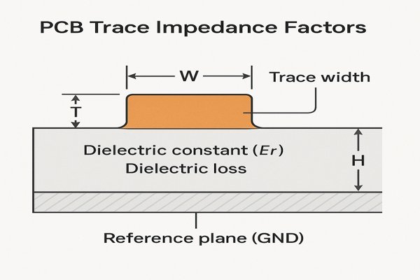
PCB trace impedance is primarily dictated by the physical cross-sectional geometry of the trace (its width and thickness), the properties of the dielectric material surrounding it (its dielectric constant, \(E_{r}\), and loss tangent), and the physical separation between the trace and its reference plane(s). These factors define the distributed capacitance and inductance of the trace.
Understanding these factors is the first step. But to truly engineer robust, high-performance hardware, you must master how these variables interact, how they are affected by the manufacturing process, and how to model their impact. In my nearly 20 years leading complex hardware projects, from aerospace to photonic computing, I've learned that overlooking these details is the surest path to costly re-spins and project delays. Let's dive deep into each aspect of impedance control.
What is the characteristic impedance of a PCB trace?
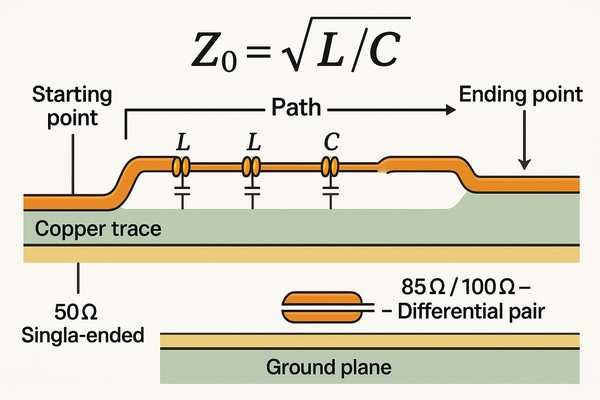
Ever wonder why your DDR interface requires a 40-ohm trace while PCIe demands 85 ohms? This isn't arbitrary. These values represent the trace's characteristic impedance, a property that governs how energy propagates along it.
Characteristic impedance (\(Z_{0}\)) is a transmission line property defined by its distributed inductance (\(L\)) and capacitance (\(C\)) per unit length as \(Z_{0} = \sqrt{\frac{L}{C}}\). For most digital applications, common standards are \(50 \text{ }\Omega\) for single-ended signals and \(85 \text{ }\Omega\), \(90 \text{ }\Omega\), or \(100 \text{ }\Omega\) for differential pairs.
Common High-Speed Interface Impedance Standards
Different high-speed interfaces are optimized for specific impedance values to ensure signal integrity and interoperability.
| Interface Standard | Impedance Type | Target Impedance (\(\Omega\)) |
|---|---|---|
| Coaxial (RF/Test) | Single-Ended | 50 or 75 |
| USB (Full/High Speed) | Differential | \(90 \pm 15\%\) |
| PCIe (Gen 3/4/5) | Differential | \(85 \pm 10\%\) |
| SATA/SAS | Differential | \(100 \pm 15\%\) |
| DDR4/5 Memory | Single-Ended | 40 or 50 (Varies) |
Applying Impedance Concepts to Power Delivery Networks
While this article focuses on signal integrity (SI), where we need to match impedance, the concept is also critical in Power Integrity (PI)1. For a Power Delivery Network (PDN), the goal is the opposite: to achieve the lowest possible impedance (e.g., milliohms) over a wide frequency range. The most advanced analysis involves Power-Aware SI, where we simulate how noise on the low-impedance PDN can introduce jitter into a high-speed signal by modulating the voltage rails of the output driver.
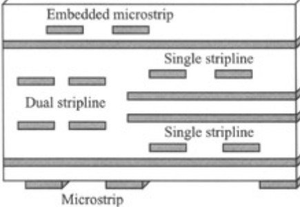
How to calculate trace impedance for a microstrip vs. a stripline?
Relying on a fabricator's generic online calculator is a risky shortcut. Accurate impedance calculation requires a deep understanding of the trace configuration and the use of professional tools.
Impedance is calculated using approximation formulas or field solvers. For a microstrip (outer layer), the classic IPC-2141A formula is \(Z_{0} \approx \frac{87}{\sqrt{E_{r} + 1.41}} \ln\left(\frac{5.98H}{0.8W + T}\right)\). For a stripline (inner layer), the formula is \(Z_{0} \approx \frac{60}{\sqrt{E_{r}}} \ln\left(\frac{4B}{0.67\pi(0.8W + T)}\right)\), where \(W\), \(H\), \(T\), and \(B\) are geometric parameters.
Modern engineering relies on electromagnetic field solvers for accurate results.
Selecting the Right Tool for Impedance Calculation
Not all solvers are created equal. The choice depends on the complexity of the geometry.
- 2D/2.5D Field Solvers: These are fast and extremely accurate for uniform transmission lines like microstrips and striplines. They work by solving Maxwell's equations for a 2D cross-section and are integrated into most PCB layout tools and standalone calculators like Polar Si9000e.
- 3D Full-Wave Solvers: For complex 3D structures like via transitions, connector breakouts, or serpentine delay lines, a 2D solver is inadequate. These require a full 3D solver (e.g., Ansys HFSS, CST Studio Suite) that can model how fields radiate and couple in all directions. These are computationally intensive but essential for \(>10 \text{ Gbps}\) design verification.
Comparing Microstrip and Stripline Configurations
| Feature | Microstrip | Stripline |
|---|---|---|
| Location | Outer Layer | Inner Layer |
| Reference Planes | One | Two |
| EMI Shielding | Fair (radiates energy) | Excellent (field is contained) |
| Propagation Speed | Faster (due to lower \(E_{eff}\)) | Slower (by \(\approx 15-20\%\)) |
How does the PCB layer stack-up influence trace impedance?
The PCB stack-up is not just a mechanical drawing; it's an electrical specification that forms the foundation of your entire signal integrity strategy. Getting it wrong means your design is flawed from the start.
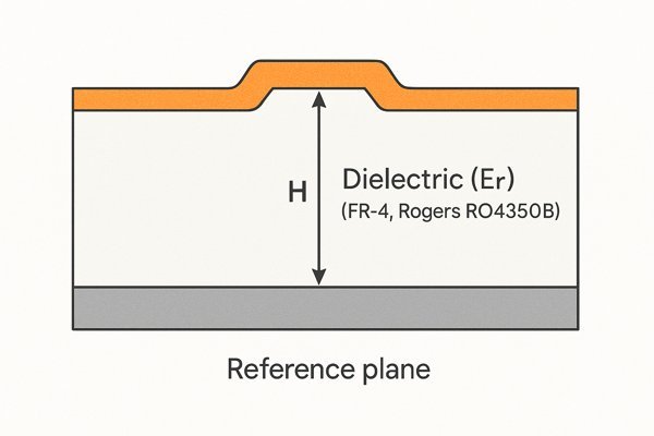
The stack-up dictates impedance through two key parameters used in impedance formulas: the dielectric constant (\(E_{r}\)) of the PCB material (e.g., standard FR-4 \(\approx 4.5\), high-speed Rogers RO4350B \(\approx 3.5\)) and the dielectric height (\(H\)) between the trace and its reference plane. A lower \(E_{r}\) or a larger \(H\) requires a wider trace to achieve the same impedance.
A professional stack-up design goes far beyond a single \(E_{r}\) value.
How Frequency Affects Dielectric Material Properties
The dielectric constant (\(E_{r}\))2 and Loss Tangent (\(\tan(\delta)\))3 of PCB materials are not constant; they vary with frequency. This is especially true for standard FR-4.
| Frequency | Typical FR-4 (\(E_{r}\)) | Typical FR-4 (\(\tan(\delta)\)) | High-Speed Material (\(E_{r}\)) | High-Speed Material (\(\tan(\delta)\)) |
|---|---|---|---|---|
| 1 GHz | 4.5 | 0.020 | 3.5 | 0.004 |
| 5 GHz | 4.3 | 0.025 | 3.48 | 0.004 |
| 10 GHz | 4.1 | 0.030 | 3.48 | 0.005 |
The Physics Governing Frequency-Dependent Effects
This frequency dependence isn't arbitrary. It's governed by a fundamental physical principle of causality (an effect cannot precede its cause), mathematically described by the Kramers-Kronig relations4. These relations dictate that the dielectric constant (the real part of permittivity) and the loss tangent (related to the imaginary part) are intrinsically linked. This is why materials engineered for low loss inherently exhibit a more stable dielectric constant over a wide frequency range, making them essential for broadband applications.
Mitigating the Fiber Weave Effect in High-Speed Laminates
At high frequencies, the weave of the glass fabric in FR-4 can cause localized impedance variations of \(5-10 \text{ }\Omega\). The choice of glass style is a critical design decision.
| Glass Style | Weave Type | SI Risk (at \(>10 \text{ GHz}\)) | Mitigation |
|---|---|---|---|
| 1080 | Standard | High | Avoid for critical nets |
| 3313 | Tighter | Medium | Better, but still has weave effect |
| 1067 | Spread | Low | Good high-speed choice |
| No Glass | Homogeneous | Very Low | Best performance (e.g., PTFE laminates) |
To combat this, I often specify materials with mechanically spread glass or rotate the entire routing on a critical layer by \(\approx 10 \text{ degrees}\) to average out the effect.
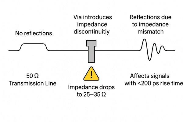
How do vias affect signal impedance?
A via is not a simple wire; it's a complex 3D structure that often represents the single largest impedance discontinuity on a high-speed path. For a 28 Gbps signal, a poorly designed via is a dead end.
A via introduces a capacitive impedance dip, often dropping a \(50 \text{ }\Omega\) line to \(25-35 \text{ }\Omega\) over its length. This discontinuity is modeled as a PI network (\(C_{pad}-L_{barrel}-C_{pad}\)) and can be estimated with formulas like \(C_{via} \approx \frac{1.41 \epsilon_{r} T D_{1}}{D_{2} - D_{1}}\), causing reflections for signals with rise times \(< 200 \text{ ps}\).
Modeling a Via's Parasitic Effects
A via's behavior is dominated by its physical components, each contributing a parasitic effect.
| Via Component | Primary Parasitic Effect | Impact on Signal |
|---|---|---|
| Entry/Exit Pads | Shunt Capacitance5 | Slows rise time, creates impedance dip |
| Via Barrel | Series Inductance | Can create an impedance spike, limits current flow |
| Antipad | Reduces Shunt Capacitance | Helps raise via impedance closer to target |
| Via Stub | Resonant Stub | Creates nulls (suck-outs) in frequency response |
Strategies for Mitigating Via Discontinuities
Engineers employ several strategies, each with performance and cost trade-offs.
| Strategy | Description | Performance Benefit | Relative Cost |
|---|---|---|---|
| Return Path Vias | Placing ground vias near signal vias. | Good (provides short return path) | Low |
| Back-Drilling6 | Removing the unused via stub. | Excellent (eliminates stub resonance) | Medium |
| Microvias (HDI) | Using laser-drilled, smaller vias. | Best (lowest parasitic C and L) | High |
Do component pads break impedance control?
You can have a perfect \(50 \text{ }\Omega\) trace, but the moment it hits a component pad, that control is broken. This transition point is a critical and often overlooked source of reflections.
Yes, a component pad acts as a shunt capacitor, creating an impedance discontinuity. For example, a standard 0402 pad adds approximately \(0.25 \text{ pF}\) of capacitance, which can cause the local impedance of a \(50 \text{ }\Omega\) trace to drop \(< 40 \text{ }\Omega\). This mismatch causes reflections, especially for signals \(>1-2 \text{ GHz}\).
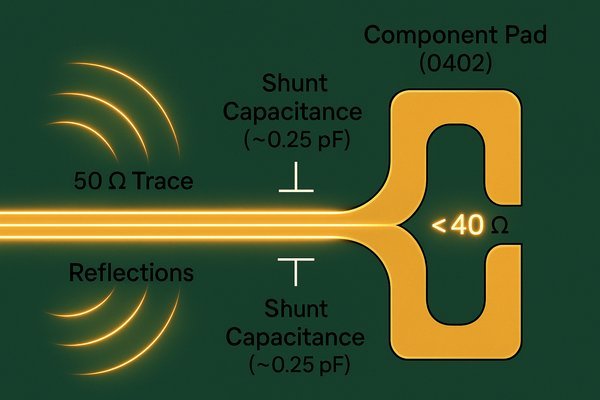
Understanding the Capacitive Effect of Component Pads
The extra copper area of a pad relative to the trace increases the capacitance to the reference plane below it, causing a localized dip in impedance.
| Package | Typical Pad Capacitance |
|---|---|
| 0402 | \(\approx 0.25 \text{ pF}\) |
| 0201 | \(\approx 0.10 \text{ pF}\) |
| BGA Pad | \(\approx 0.3 - 0.5 \text{ pF}\) |
Advanced Techniques for Compensating Pad Capacitance
For high-speed designs, this capacitance must be counteracted.
- Neck-Down Routing: Tapering the trace as it enters the pad is the simplest form of compensation.
- Inductive Compensation via Reference Plane Voiding: The professional solution is to create a cutout (void) in the reference plane directly beneath the pad. This reduces the pad's capacitance and adds series inductance. By carefully sizing the void, this added inductance can be tailored to cancel out the excess pad capacitance. This technique requires a 3D field solver to implement correctly.
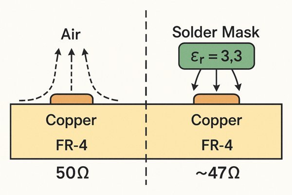
How does solder mask affect the final impedance of a trace?
For designs requiring tight impedance tolerance (e.g., \(\pm 5\%\)), ignoring the solder mask is a recipe for failure. It's a thin layer, but its electrical properties are significant.
Solder mask lowers microstrip impedance by acting as an additional dielectric. A standard LPI solder mask (\(E_{r} \approx 3.3\)) with a thickness of \(0.8-1.0 \text{ mil } (20-25 \text{ }\mu\text{m})\) will reduce a calculated \(50 \text{ }\Omega\) trace to a final impedance of approximately \(47-48 \text{ }\Omega\). This must be pre-compensated for in tight tolerance designs.
Understanding the Electrical Impact of Solder Mask
The solder mask's dielectric constant and thickness add to the overall distributed capacitance of an outer-layer trace, which directly lowers its impedance.
| Parameter | Calculated Impedance (No Mask) | Final Impedance (With Mask) |
|---|---|---|
| Single-Ended | \(50.0 \text{ }\Omega\) | \(\approx 47.5 \text{ }\Omega\) |
| Differential | \(100.0 \text{ }\Omega\) | \(\approx 95.0 \text{ }\Omega\) |
Solder Mask Considerations for High-Frequency Designs
The thickness of the solder mask is not perfectly uniform; it can vary by \(\pm 0.2-0.3 \text{ mils}\) across a panel, contributing to your total impedance tolerance budget. For cutting-edge applications like 77 GHz automotive radar, the high loss tangent of solder mask is unacceptable. In these cases, we specify a "solder mask relief," leaving the critical RF traces completely uncovered to ensure maximum performance and consistency.
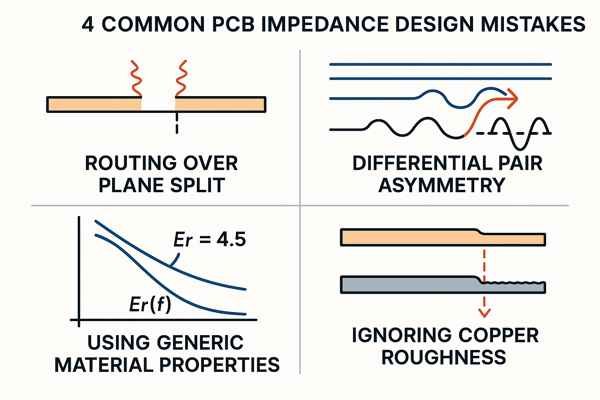
What Are the Common Mistakes Made in PCB Impedance Design?
Experience is often learning from mistakes. Here are some of the most destructive—and common—errors I've had to troubleshoot in my career.
A summary of these critical design flaws highlights their severity.
| Mistake | Consequence | Severity |
|---|---|---|
| Routing Over Split Plane | Massive impedance spike, severe EMI radiation. | Critical |
| Differential Pair Asymmetry | Skew and mode conversion, leading to EMI and crosstalk. | Critical |
| Using Generic \(E_{r}\) | Incorrect impedance calculation, reflections. | High |
| Ignoring Conductor Losses | Underestimated signal loss (attenuation), closed eye diagram. | High |
Mistake 1: Routing Over a Reference Plane Split
This remains the cardinal sin of high-speed PCB design. A high-speed signal's return current wants to follow the path of least inductance, which is directly underneath the signal trace in the reference plane. If you route the trace over a split or gap in that plane (e.g., between a digital ground and an analog ground), you force the return current to make a long detour to find a path back. This creates a massive current loop, which dramatically increases the inductance of that trace section. Since impedance is proportional to inductance (\(Z_{0} = \sqrt{L/C}\)), this causes a huge impedance spike, leading to severe signal reflections. Furthermore, this large current loop acts as a highly efficient antenna, radiating significant electromagnetic energy and almost guaranteeing a failure during EMC/EMI compliance testing.
Mistake 2: Ignoring Differential Pair Asymmetry
The primary benefit of a differential pair is its tight electromagnetic coupling, which allows it to reject common-mode noise. This benefit depends entirely on perfect symmetry. Any asymmetry in the pair—such as one trace being slightly longer than the other while navigating a bend, or one trace being routed closer to a ground plane—introduces two major problems. First, it creates timing skew7, where the two signals arrive at the receiver at slightly different times. Second, and more insidiously, it causes mode conversion. This is where energy from the desired differential signal is converted into unwanted common-mode noise. This common-mode energy is no longer rejected by the receiver and can radiate very effectively from the traces, causing crosstalk to adjacent signals and contributing to EMI.
Mistake 3: Using Generic Material Data
A common shortcut is to use a single, nominal value for a material's dielectric constant (\(E_{r}\)), such as 4.5 for standard FR-4. This is a significant mistake because, as shown in previous sections, \(E_{r}\) is not a constant; it decreases as frequency increases. A datasheet value is often specified at a low frequency like 1 MHz. A high-speed digital signal, however, is broadband and contains a wide spectrum of frequency components. If you calculate your trace width based on an \(E_{r}\) of 4.5, the actual impedance at higher frequencies (where the effective \(E_{r}\) might be 4.1) will be significantly higher than your target. This frequency-dependent impedance mismatch causes reflections and distortion. The only reliable method is to use the frequency-dependent material models provided by the laminate manufacturer for use in a modern field solver.
Mistake 4: Failing to Model Conductor Losses
At high frequencies, the loss (or attenuation) of a signal traveling down a trace is dominated by two conductor effects that go beyond simple DC resistance: the skin effect8 and copper roughness.
- Skin Effect: As frequency increases, the current begins to flow only on the outer surface, or "skin," of the conductor. This reduces the effective cross-sectional area available for current flow, increasing the trace's resistance. This loss is proportional to the square root of the frequency.
- Copper Roughness: To ensure good adhesion between the copper foil and the dielectric material, the copper surface is intentionally roughened. At multi-gigahertz frequencies, the skin depth becomes so small that the current is forced to follow this jagged, microscopic path. This increases the effective path length compared to a perfectly smooth trace, further increasing the conductor's resistance and loss.
Ignoring these effects leads to a wildly optimistic calculation of insertion loss (\(S_{21}\))9. You might simulate a perfectly open eye diagram, but on the real board, the signal reaching the receiver is too attenuated to be correctly interpreted, resulting in system failure.
How to specify impedance control requirements for a PCB manufacturer?
A verbal agreement or a vague note is not enough. Your fabrication drawing is a legal document. It must be explicit, complete, and unambiguous.
Specify impedance in fab notes with a table defining: 1) The target impedance and type (e.g., \(100 \text{ }\Omega\) Differential); 2) The required tolerance (e.g., \(\pm 7\%\)); 3) The specific layers and net names it applies to; and 4) A requirement for TDR verification on a test coupon included on the panel.
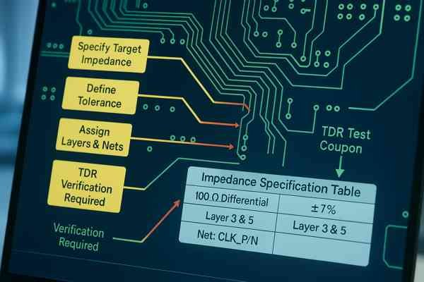
The Fabrication Drawing as a Technical Contract
A professional fab drawing goes beyond a simple table. You must provide a reference stack-up and explicitly permit the fabricator to adjust trace geometries to meet impedance targets with their specific process. The note is key: "FABRICATOR MAY ADJUST TRACE GEOMETRIES TO MEET IMPEDANCE. FINAL STACK-UP REQUIRES ENGINEERING APPROVAL PRIOR TO FABRICATION."
Specifying Key Information in Fabrication Notes
Your impedance control table should be clear and concise.
| Item | Specification |
|---|---|
| Target Impedance | \(85 \text{ }\Omega\) Differential |
| Tolerance | \(\pm 7\%\) |
| Applicable Layers | L3, L5, L8 (PCIe Lanes) |
| Net Names | PCIE_TX_*, PCIE_RX_* |
| Test Method | 4-Port TDR Verification using Coupon C1 |
How is the impedance of a manufactured PCB verified?
"Trust, but verify" is the mantra for high-reliability hardware. A TDR report is the primary evidence that your board was manufactured to your electrical specification.
Impedance is verified using a Time-Domain Reflectometer (TDR) on a test coupon manufactured on the same panel. The TDR measures the impedance profile along the test trace. The fabricator must provide a report showing the TDR plot and confirming the average measured impedance falls within the specified tolerance (e.g., \(46.5 \text{ to } 53.5 \text{ }\Omega\) for a \(50 \text{ }\Omega \pm 7\%\) requirement).
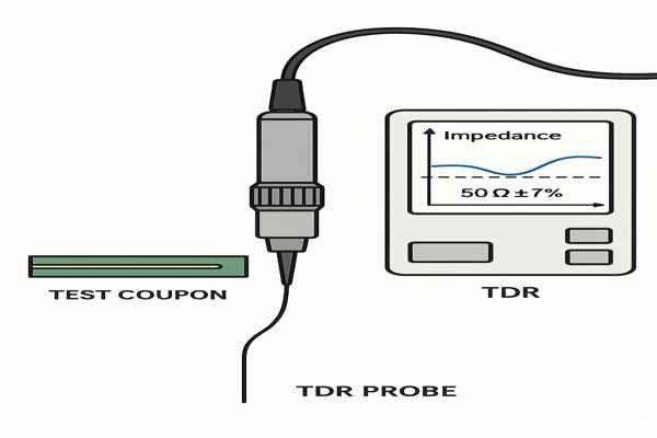
How to Read a Time-Domain Reflectometer (TDR) Report
When I review a TDR report, I look for more than just the average impedance value. The shape of the plot tells a story about the transmission line quality.
| TDR Plot Feature | Indicates | Potential Cause |
|---|---|---|
| Downward Dip | Capacitive Discontinuity | Wide spot in trace, component pad, via pad |
| Upward Peak | Inductive Discontinuity | Narrow spot in trace, via barrel, connector pin |
| Gradual Slope | Lossy Trace | High dielectric or conductor loss |
| Overall Shift | Process Variation | Incorrect dielectric height or trace width |
Using Advanced TDR Diagnostics for Deeper Insight
Some advanced test services can even extract the distributed inductance (\(L\)) and capacitance (\(C\)) from the TDR measurement. This is invaluable for diagnostics, as it can tell you why the impedance is off (e.g., "impedance is low because capacitance is high, suggesting the dielectric is too thin").
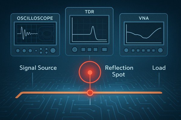
How to troubleshoot signal integrity problems caused by impedance mismatch?
When a prototype fails on the bench, a systematic approach combining simulation and measurement is the only way to efficiently find the root cause.
Troubleshoot by: 1) Using a high-bandwidth oscilloscope to check for reflections, ringing, and a closed eye diagram. 2) Using a TDR to physically locate the impedance mismatch on the trace. 3) Using a Vector Network Analyzer (VNA) to characterize frequency-dependent performance after proper calibration.
Step 1: Observe the Effect with an Oscilloscope
The first step is to identify the symptoms of a signal integrity problem on the scope.
| Observation on Scope | Likely Signal Integrity Problem |
|---|---|
| Ringing, Overshoot/Undershoot | Impedance mismatch causing reflections. |
| Slow or Non-Monotonic Rise Time | Excessive capacitance or high channel loss. |
| Closed or "Dirty" Eye Diagram | Combination of loss, reflection, and jitter. |
Step 2: Localize and Characterize the Cause with a TDR/VNA
These tools provide a complete picture of the channel's performance.
| Tool | Domain | Key Measurement | What It Tells You |
|---|---|---|---|
| TDR | Time | Impedance vs. Distance | Where the physical discontinuity is located |
| VNA | Frequency | Return Loss (\(S_{11}\))10 | How much mismatch exists at each frequency |
| VNA | Frequency | Insertion Loss (\(S_{21}\)) | How much signal is lost (attenuated) |
A good rule of thumb is that the return loss (\(S_{11}\)) should be \(< -10 \text{ dB}\) across your frequency band of interest.
Step 3: Ensure Measurement Accuracy with De-embedding11
Raw VNA measurements include the electrical effects of the cables, probes, and connectors used to test the board. To measure only the device under test (DUT), these effects must be removed through a process called de-embedding. This is done by first performing a precise calibration using known standards, such as a TRL (Thru-Reflect-Line) or SOLT calibration kit. Failing to de-embed properly can lead to completely misleading results.
Conclusion
Controlling PCB impedance is a core discipline of modern hardware engineering. It requires moving beyond simple rules of thumb to a deep understanding of frequency-dependent material properties, manufacturing effects, and the trade-offs between signal integrity and power integrity. Master these details, and you can build robust, reliable products that work the first time.
-
Understanding Power Integrity is crucial for ensuring stable power delivery in high-speed circuits, enhancing overall system performance. ↩
-
Learn how the dielectric constant (E_r) impacts signal integrity and performance in PCB materials, especially for high-speed and RF applications. ↩
-
Understanding Loss Tangent is crucial for optimizing material performance in high-frequency applications. ↩
-
Explore the Kramers-Kronig relations to grasp the fundamental physics behind dielectric behavior in materials. ↩
-
Understanding Shunt Capacitance is crucial for optimizing circuit performance and mitigating signal issues. ↩
-
Exploring Back-Drilling can help you learn how to eliminate unwanted resonances and improve signal integrity. ↩
-
Learn how timing skew impacts high-speed differential signals and discover best practices to minimize skew for reliable PCB performance. ↩
-
Discover how skin effect impacts signal integrity at high frequencies in PCB designs. ↩
-
Learn how insertion loss (S21) affects signal integrity in high-speed PCBs and why accurate modeling is crucial for reliable circuit performance. ↩
-
Learn how return loss (S11) reveals impedance mismatches and why maintaining low S11 is crucial for high-quality signal transmission in your designs. ↩
-
Exploring de-embedding will enhance your measurement accuracy and ensure reliable results in your testing. ↩


