 Skip to content
Struggling to connect boards reliably? A poor connection can lead to system failure and endless debugging headaches. Edge connectors offer a robust, industry-standard solution for board-to-board communication.
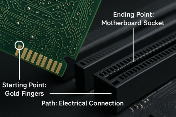
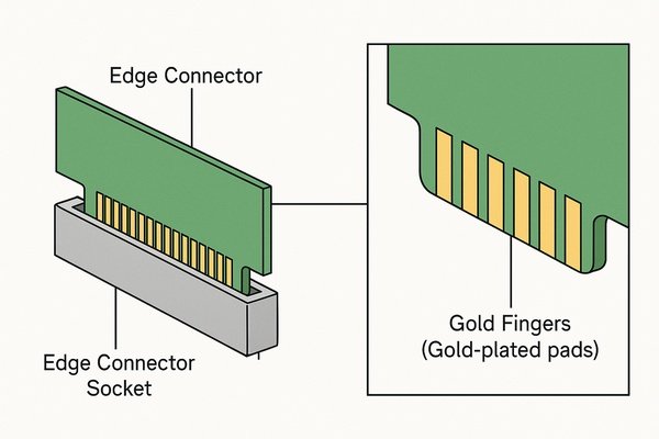
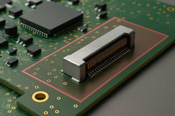
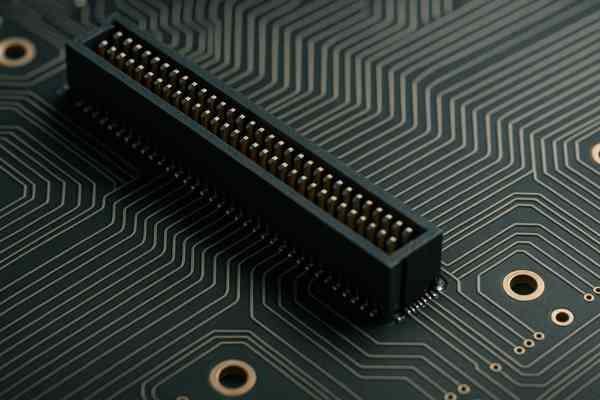
An edge connector is a system that creates an electrical connection using a pattern of conductive traces, known as gold fingers, along the edge of a Printed Circuit Board (PCB). These fingers mate with a corresponding socket on a motherboard or backplane, enabling communication and power transfer.
An edge connector is more than just the shiny pads on a graphics card. It's a precise electromechanical system. Understanding the details of this system is crucial for any hardware engineer designing modular electronics. It involves everything from the layout of the PCB itself to the material science of the mating socket. In this post, I'll dive deep into the critical aspects of designing with edge connectors, sharing insights from my nearly 20 years of experience to help you avoid common pitfalls and ensure your designs are robust and reliable.
What are the differences between edge connectors and gold fingers?
Confusing these two terms can lead to miscommunication with your PCB fabricator. Getting the terminology wrong can result in costly errors and project delays. It’s essential to be precise.
The "edge connector" refers to the entire interconnection system, which includes both the PCB pads and the mating socket. "Gold fingers" specifically describe the gold-plated copper pads located on the edge of the PCB that make direct contact with the socket's pins.
The manufacturing process itself reveals further distinctions. Gold fingers require Hard Electrolytic Gold plating, typically 30 to 50 micro-inches (µin) of gold over 100 to 200 µin of nickel, per IPC-60121. The underlying nickel layer is a diffusion barrier preventing copper migration. If this layer is compromised or the gold is porous due to poor plating bath control, you risk nickel corrosion and increased contact resistance. On the mating socket, SMT pads often use ENIG. However, if this immersion gold is too thick (above ~4 µin), it can cause gold embrittlement of the solder joint, a critical defect identified in IPC-J-STD-0012. The pad geometry is also engineered for contact sequencing in hot-pluggable systems like PCIe, ensuring ground pins mate first. This staggered profile is a critical part of the standard, not an arbitrary layout.
Gold Fingers as a Component in the Edge Connector System
| Feature | Edge Connector | Gold Fingers |
|---|---|---|
| Scope | The entire electromechanical system (pads + socket) | A PCB feature with specific plating, geometry, and sequencing |
| Function | To create a removable, reliable electrical link | To provide a durable, sequenced, low-resistance contact surface |
| Key Standard | PCI-SIG CEM3 Spec, SFF-8639, etc. | IPC-6012 (Class 2 or 3), IPC-45524 (ENEPIG) |
| Failure Modes | Housing warp, pin fatigue, contact resistance rise | Plating wear-through, nickel corrosion, pad delamination |
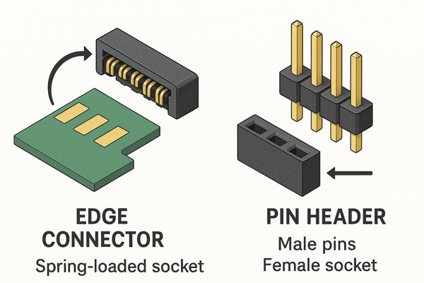
What are the differences between an edge connector and a pin header?
Choosing the right board-to-board connection is a critical design decision. The wrong choice can impact your product's cost, durability, high-speed performance, and even its physical size.
An edge connector uses flat, gold-plated pads on the PCB edge that mate with a spring-loaded socket, making it ideal for high-speed signals and frequent insertions. A pin header uses male pins on one board mating with a female socket on another, a lower-cost solution for semi-permanent connections.
In high-vibration environments, the failure modes differ significantly. Pin headers are highly susceptible to fretting corrosion5. Micro-movements between the male pin and female socket abrade the thin plating, exposing the base copper or bronze. This exposed metal oxidizes, forming an insulating layer that leads to intermittent and eventually permanent connection failure. The high contact force and large, flat contact area of an edge connector inherently resist this fretting motion. For ruggedized systems used in military or transportation applications, connectors are qualified against specific shock and vibration profiles, such as MIL-STD-810G6. An edge connector system is often designed to meet these stringent requirements, sometimes categorized by a VITA standard, whereas a standard pin header would fail almost immediately.
Key Trade-Offs: Edge Connectors vs. Pin Headers
| Feature | Edge Connector | Pin Header |
|---|---|---|
| Mating Cycles | High (e.g., 250 to 500+) | Low (e.g., 10 to 50) |
| Vibration Resistance | High; resistant to fretting corrosion | Poor; prone to fretting and failure |
| Typical Inductance | 200-500 pH | 2-5 nH |
| Impedance Control | Tightly controlled (e.g., 85Ω ±5%) | Uncontrolled (70-130Ω variation) |
| Ruggedization | Can be designed to meet MIL-STD standards | Not suitable for high-shock/vibration |
| Cost | Higher | Lower |
What are the PCB layout and routing guidelines for high-speed edge connectors?
High-speed signals are unforgiving. Poor layout practices in the breakout region of an edge connector will degrade your signal, causing bit errors and system failure. Following strict rules is not optional.
Key guidelines include maintaining a consistent impedance profile, using back-drilling to eliminate via stubs, ensuring a continuous ground return path, and managing symmetry to prevent mode conversion.
An advanced technique for the breakout region involves optimizing the shape of the anti-pad7. For speeds exceeding 25 Gbps, a simple circular void in the ground plane around a via is not optimal. A more refined approach is to use "coffin-shaped" or elliptical anti-pads, which are tuned using a 3D field solver. This shaping provides a more gradual impedance transition from the planar trace to the vertical via structure, reducing reflections. Furthermore, the PCB stack-up itself plays a role. Using thinner dielectric layers between the signal and its reference plane allows for narrower trace widths for a given impedance (e.g., 50Ω). This makes it physically easier to route traces out from a dense, fine-pitch connector pin field without violating trace-to-trace spacing rules, a common challenge in modern designs.
Critical Layout Rules for Signal Integrity
| Guideline | Specification | Rationale |
|---|---|---|
| Impedance Profile | Maintain target (e.g., 85Ω) with geometries from a 2D/3D field solver. | Minimize reflections (Return Loss8). |
| Via Stub Removal | Back-drill stubs to be < 8 mils for 25+ Gbps signals. | Eliminates resonant nulls in the insertion loss9 profile. |
| Return Path Vias | Place ground vias within ~20 mils of every high-speed signal via. | Provides a low-inductance path for return currents, preventing large current loops. |
| Anti-Pad Shaping | Use optimized shapes (e.g., coffin) for anti-pads in ultra-high-speed breakouts. | Provides a smoother impedance transition from trace to via. |
What is the required PCB edge chamfer angle and tolerance for proper insertion?
Forcing a PCB into a tight connector socket is a recipe for disaster. This can damage the connector's delicate pins or even crack the PCB, leading to costly rework or scrap.
A beveled edge, or chamfer, is required to guide the PCB smoothly into the socket. For most standard connectors like PCIe, a 30° or 45° chamfer is specified, with a typical angle tolerance of ±5°. The leading depth of the chamfer is also critical.
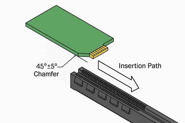
A subtle but important detail is the interaction between the chamfer and the first row of electrical contacts. The connector standard defines a "setback" distance from the leading edge of the PCB to the start of the first contact pad. If the chamfer is cut too deep, it can encroach on this setback and reduce the available surface area of the first row of pads. This can compromise the mechanical adhesion of these pads and, for power pins, slightly reduce their current-carrying capacity. Therefore, it's critical to verify that your specified chamfer depth (D) and angle (A) do not violate the minimum pad area requirements derived from the connector's mechanical specification. Always include a detailed mechanical drawing in your Gerbers.
Understanding and Specifying PCB Edge Chamfers
| Parameter | Typical Value | Tolerance | Rationale |
|---|---|---|---|
| Chamfer Angle | 45° | ±5° | Guides insertion, prevents stubbing. |
| Chamfer Depth | 1.0mm - 2.0mm | ±0.2mm | Balances ease of insertion with preserving pad area. |
| Edge Quality | Smooth, free of burrs | - | Prevents contamination and short circuits. |
What are the standard mechanical "keep-out" zones around a press-fit or SMT edge connector socket?
Placing a component too close to your edge connector socket can create a nightmare. It can interfere with the mating card, block assembly tooling, or make future rework impossible.
Keep-out zones are areas where no components, vias, or sometimes even traces should be placed. These are defined not just by mechanical fit but also by safety, testability, and secondary manufacturing processes.
A critical but often overlooked consideration is high-voltage keep-out. For medical, industrial, or power system applications, safety standards like IEC 60601-110 or UL 61010-1 mandate specific minimum distances for creepage (along a surface) and clearance (through the air)11 between high-voltage circuits and low-voltage or chassis ground circuits. These required safety keep-outs can be much larger—sometimes 8mm or more—than the mechanical keep-outs. They may even require milling physical slots or trenches in the PCB within the connector's footprint to increase the surface path distance and meet safety regulations. These requirements supersede all other mechanical placement rules.
Planning Keep-Outs for Assembly, Test, and Safety
| Keep-Out Type | Typical Dimension | Purpose |
|---|---|---|
| Component Fit | 1.5mm | Prevents physical interference with connector body. |
| Press-Fit Tooling | 10-15mm (bottom) | Provides clearance for the assembly arbor press. |
| Safety (Creepage) | >8mm (HV) | Meets safety standards like IEC 60601-1. |
| Test Probe Access | ~5mm | Allows for probing signals during debug. |
| Coating/Underfill | ~3mm | Provides clearance for manufacturing nozzles. |
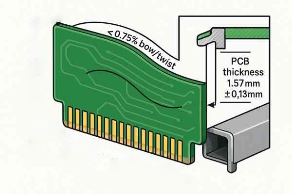
How is the Z-axis tolerance of a PCB specified to ensure proper contact with the connector pads?
You've designed the perfect circuit, but your product suffers from intermittent failures. The cause might be something as simple as the thickness of your PCB being out of spec, causing a poor connection.
Z-axis tolerance, or the final thickness of the PCB, is critical. For standard edge connectors like PCIe, the required thickness is 1.57mm (0.062 inches) with a tight tolerance of ±0.13mm (±0.005 inches), or about ±8%. Additionally, flatness (bow and twist) must be controlled to < 0.75%.
A long-term reliability concern related to the PCB laminate is Conductive Anodic Filament (CAF) formation12. CAF is an electrochemical process where conductive filaments grow along the interface between the glass fibers and the resin system of the laminate. Under conditions of high humidity and DC voltage bias, these filaments can grow between adjacent plated through-holes, eventually causing a short circuit. The risk of CAF is higher in dense designs with small hole-to-hole spacing. To mitigate this, engineers working on long-life, high-reliability products specify laminates with superior CAF resistance, which typically involves a tighter glass weave and an advanced resin chemistry. This is a prime example of how a material selection decision directly impacts the long-term electrochemical reliability of the product.
Specifying PCB Thickness, Flatness, and Material Weave
| Parameter | Specification | Rationale |
|---|---|---|
| Finished Thickness | 1.57mm ±0.13mm | Ensures proper contact force in the connector. |
| Bow and Twist | < 0.75% per IPC-A-60013 | Guarantees the board is flat enough for uniform contact. |
| Laminate Selection | Specify high CAF resistance for high-rel products | Prevents long-term short-circuit failures in humid environments. |
How do you model the impedance profile of an edge connector for simulation?
For high-speed digital design, you can't just hope your channel will work. "Hope" is not a design strategy. You must simulate the entire channel, and that requires an accurate model of every component, including the connector.
The most accurate way is a full-channel simulation using cascaded S-parameter models for all passive components and IBIS-AMI (Algorithmic Modeling Interface) models for the active SerDes transceivers. The final step is to correlate this simulation with physical measurements.

The ultimate validation of your models and your design is simulation-to-measurement correlation14. After building the first prototypes, a crucial step is to measure the physical hardware. This involves using a Vector Network Analyzer (VNA)15 to measure the S-parameter16s of the actual PCB traces and connector assembly. You then compare the measured data to your simulated S-parameter data. If there are significant discrepancies, it indicates a problem in either your simulation models (e.g., incorrect material properties) or your manufacturing process (e.g., incorrect trace widths or layer thickness). Additionally, a Time-Domain Reflectometer (TDR)17 can be used to send a pulse down the physical trace, and the reflections can be mapped to specific physical locations, allowing you to pinpoint exactly where the impedance discontinuities that your simulation predicted are located.
A Professional Workflow for Channel Simulation and Validation
- Simulate: Build the full channel using IBIS-AMI models for the SerDes and S-parameter models for all passives (PCB traces, vias, connectors).
- Measure: Use a VNA to measure the S-parameters of a physical prototype. Use a TDR to locate discontinuities.
- Correlate: Compare the simulated S-parameters and TDR plots to the measured results.
- Iterate: If they don't match, refine your models or investigate your manufacturing process until correlation is achieved. This builds confidence that your simulations accurately predict reality.
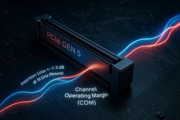
What are typical insertion loss and return loss values for a Gen 5 PCIe connector?
When designing for bleeding-edge speeds like PCIe Gen 5 (32 GT/s), every decibel of signal loss matters. Your components must meet stringent performance targets to ensure the link can function without errors.
For a PCIe Gen 5 compliant connector, the insertion loss should be less than -1.5 dB at the Nyquist frequency of 16 GHz. However, modern compliance has moved beyond simple loss metrics to a more holistic analysis called Channel Operating Margin (COM).
It is important to understand the concept of loss budgeting across the channel. The PCI-SIG specification provides a normative (required) loss budget for the entire channel, but the individual loss values for components like the connector or a specific length of trace are often informative (a guideline). This allows for engineering trade-offs. For example, if your design requires a longer-than-usual PCB trace, incurring extra loss, you can compensate by selecting a connector with exceptionally low loss and by using an ultra-low-loss PCB laminate material like Megtron 7 instead of a standard material. The goal is not for every single piece to be the absolute best, but for the sum of all losses and reflections in the system to meet the overall COM target. This system-level approach is key to cost-effective high-speed design.
Moving Beyond Loss to Channel Operating Margin (COM)
| Parameter | Source | Significance |
|---|---|---|
| Channel S-parameters | 3D Field Solver / VNA Measurement | Describes the physical behavior of the passive channel. |
Transceiver *.cfg | Chip Vendor | Defines the equalization and noise/jitter performance. |
| COM Script | PCI-SIG | The standardized algorithm that performs the calculation. |
| COM Result | > 3 dB (Pass) | A holistic, statistical pass/fail for the entire link. |
Where can I find S-parameter or IBIS models for a specific edge connector part number?
You're ready to run your high-speed simulation, but you can't find the model for your connector. This can be a frustrating roadblock that delays your entire design verification process.
The primary and most reliable source for simulation models is the connector manufacturer's website. If a model is unavailable for a critical component, you must have one created using a 3D full-wave electromagnetic solver or by professional measurement.

If you are forced to create your own model for a connector, it is a non-trivial task. It requires using a 3D full-wave electromagnetic solver like Ansys HFSS or CST Microwave Studio. The process involves:
- Obtaining a detailed 3D mechanical model (e.g., a STEP file) of the connector.
- Importing the model and meticulously assigning the correct material properties (Dk, Df for plastics; conductivity for metals) to every part.
- Defining the signal ports at the exact locations where the connector will interface with the PCB traces.
- Setting up the simulation boundary conditions and running a frequency sweep, which can take many hours of computation time.
- De-embedding18 the ports to remove any artifacts from the simulation setup itself.
This highlights the immense value of the pre-made, validated models provided by reputable manufacturers.
A Practical Guide to Finding (or Creating) Models
- Go to the Source: Check the websites of Samtec, TE Connectivity, Molex, Amphenol, etc.
- Contact Support: Email their FAEs; they are a valuable resource.
- Create Your Own (If Necessary): For non-critical paths, use a simple RLC model. For critical high-speed paths, use a 3D EM solver or commission a measurement lab.
What is the maximum current rating per pin for power and ground contacts on a connector?
Powering your device through an edge connector is common, but you must respect the current limits of the pins. Overloading a pin will cause it to overheat, increasing its resistance and potentially leading to a catastrophic failure where the pin melts or deforms.
The thermal current rating (e.g., 1.5A per pin) is a baseline. You must also analyze the AC power integrity by considering the loop inductance of the power path, which is critical for managing transient current demands.
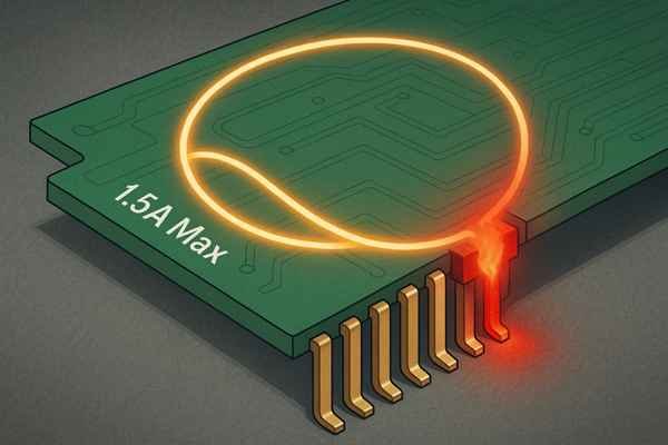
Fast-switching ICs like FPGAs draw large amounts of current in very short bursts (high di/dt). This transient current must be supplied from nearby decoupling capacitors. The path from the capacitor, through the planes, through the connector, and to the chip has a certain loop inductance19. A high inductance in the connector's power pins can impede this transient current, causing the power rail voltage at the IC to collapse temporarily. This can lead to logic errors or system resets. This is why we use many parallel power and ground pins: it's not just to lower the DC resistance for IR drop, but to create a wide, low-inductance path that can handle high-frequency transient currents. A target loop inductance for a high-performance power path through a connector should be in the sub-nH range.
Beyond Thermal Limits: DC Drop and AC Impedance Analysis
| Analysis | Key Parameter | Failure Mode | Design Goal |
|---|---|---|---|
| DC Power (Thermal) | Current Rating (Amps) | Pin overheating, melting. | Stay below derated current limit. |
| DC Power (PI) | Path Resistance (mΩ) | Excessive voltage (IR) drop. | Parallel enough pins to keep voltage drop within tolerance. |
| AC Power (PI) | Loop Inductance (nH) | Power rail collapse due to transient currents. | Create a wide, low-inductance path with many parallel pins. |
What are the best practices for minimizing crosstalk when routing multiple differential pairs into a connector?
When you pack dozens of high-speed signal pairs into a dense connector, their electromagnetic fields can couple. This interference, known as crosstalk, corrupts your data and can cause difficult-to-diagnose bit errors.
To minimize crosstalk, use wide spacing (3W-5W rule), strategic ground pin assignments in the connector, and PCB-level shielding techniques like ground guard traces. A well-designed guard trace can improve isolation by 3-6 dB.
A guard trace is a ground-referenced trace routed parallel to and between two aggressive signal traces (or pairs). For it to be effective, it must be stitched to the main ground plane with vias at regular intervals, typically no more than λ/20, where λ is the wavelength corresponding to the signal's knee frequency. However, using guard traces is a trade-off. They consume valuable routing space and can slightly complicate impedance control. They are not a panacea to be used everywhere, but rather a targeted weapon to be deployed in specific problem areas, such as isolating a high-swing clock signal from a sensitive, low-swing data bus, or protecting an analog signal from a noisy digital interface within the same connector pin field.
Advanced Techniques for Crosstalk Mitigation
| Technique | Implementation | Effectiveness |
|---|---|---|
| Spacing (3W/5W Rule) | Increase physical distance between pairs. | Fundamental and highly effective. |
| Ground Pin Shielding | Assign ground pins between critical pairs in the connector pinout. | Excellent isolation within the connector body. |
| Guard Traces | Route a ground-stitched trace between pairs on the PCB. | Targeted 3-6 dB improvement in isolation. |
| Layer Separation | Route aggressive pairs on non-adjacent layers (e.g., L3 and L5). | Provides excellent vertical isolation. |
How does the contact force of the connector's pins affect long-term reliability and resistance?
A connection that works perfectly on the test bench might fail intermittently months or years later in the field. This degradation is often due to subtle mechanical effects, where contact force plays a starring role.
Higher contact force (50 to 150 grams per contact) creates a reliable, gas-tight seal and enables sufficient contact wipe. The material of the spring contact, typically Beryllium Copper (BeCu) for high-end connectors, determines its ability to maintain this force over time and temperature.
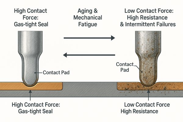
A critical material property for long-term reliability is stress relaxation. This is the tendency of a material under constant strain (like a compressed connector spring) to lose its internal stress (and thus its contact force) over time, a process that accelerates at high temperatures. Beryllium Copper20 is superior to Phosphor Bronze in this regard. For example, at 100°C, a Phosphor Bronze contact might lose 15-20% of its initial force over 1000 hours, while a BeCu contact might only lose 3-5%. This resistance to stress relaxation is why BeCu is mandated for connectors in harsh environments like automotive engine compartments or downhole drilling equipment, where a connection must remain reliable for years at elevated temperatures.
How Contact Material Science Affects Long-Term Reliability
| Material | Key Advantage | Relative Cost | Typical Application |
|---|---|---|---|
| Beryllium Copper (BeCu) | Superior spring properties, resists stress relaxation. | Higher | High-reliability, high-temp (aerospace, automotive). |
| Phosphor Bronze | Good performance, lower cost. | Lower | General commercial and consumer electronics. |
What are the material specifications for the connector housing for high-temperature reflow soldering processes?
You've just run a batch of new boards through the reflow oven, only to find that your expensive edge connector sockets have melted and deformed. This costly mistake is easily avoidable by choosing the correct material.
For lead-free reflow, the housing must be a high-temperature thermoplastic like LCP. For high-reliability designs, you must also consider the Coefficient of Thermal Expansion (CTE) mismatch between the connector, PCB, and solder joints.
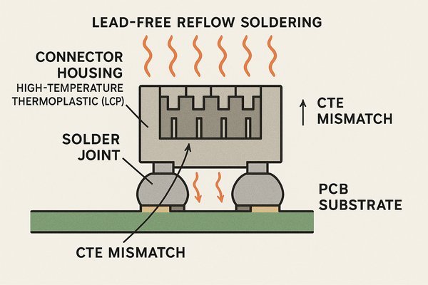
The CTE mismatch between the connector housing, its metal pins, and the FR-4 PCB creates immense stress on the SMT solder joints during temperature cycling. This can lead to low-cycle fatigue and cracked joints. To improve solder joint reliability for large connectors, advanced PCB layout techniques can be employed. Instead of a simple rectangular pad, using a "dog bone" or "home plate" shaped pad on the PCB can help optimize the solder fillet geometry. These pad shapes better control how the molten solder wicks up the pin, creating a fillet with reduced stress concentration at the heel and toe of the joint. This is a clear example of how thoughtful PCB layout can directly mitigate a mechanical failure mode, improving the product's overall thermo-mechanical reliability.
Evaluating Housing Materials for Thermal and Mechanical Stress
| Material Property | Importance | Desired Value |
|---|---|---|
| Peak Temperature | Must survive lead-free reflow (~260°C). | > 270°C |
| MSL Rating | Dictates handling requirements to prevent "popcorning". | MSL 1 (least sensitive) |
| Dielectric (Dk/Df) | Impacts signal integrity at high frequencies. | Low and stable with frequency. |
| CTE | Affects solder joint reliability under temp cycling. | Close to FR-4's CTE (~17 ppm/°C). |
Conclusion
An edge connector is a critical system, not just a set of pads. Success requires attention to mechanical details like chamfers and flatness, meticulous high-speed layout with back-drilling, and selecting materials and models for both thermal and high-frequency performance.
-
Learn how IPC-6012 sets the quality and reliability standards for gold finger plating, ensuring your PCBs meet industry requirements. ↩
-
Learn how IPC-J-STD-001 defines critical standards for solder joint quality and helps prevent defects like gold embrittlement in electronics manufacturing. ↩
-
Learn how the PCI-SIG CEM specification shapes edge connector design, ensuring compatibility and reliability in PCIe systems. ↩
-
Learn how IPC-4552 defines ENEPIG standards, ensuring reliable gold finger plating and preventing common PCB failures. ↩
-
Understanding fretting corrosion is crucial for maintaining reliable connections in high-vibration environments. ↩
-
Exploring MIL-STD-810G standards can help you ensure your connectors are rugged enough for military and transportation applications. ↩
-
Understanding anti-pad design is crucial for optimizing signal integrity in high-speed PCBs. ↩
-
Understanding return loss is crucial for minimizing signal reflections and ensuring signal integrity in high-speed PCB layouts. Learn more about its impact. ↩
-
Learn how insertion loss affects signal quality in high-speed PCBs and discover best practices to minimize it for optimal performance. ↩
-
Exploring IEC 60601-1 will provide insights into essential safety standards for medical devices, ensuring compliance and safety. ↩
-
Understanding creepage and clearance is essential for designing safe high-voltage circuits and complying with international safety standards. ↩
-
Understanding CAF formation is crucial for PCB reliability, especially in humid conditions. Explore this link to learn more. ↩
-
Learn how IPC-A-600 defines PCB acceptability, ensuring your boards meet industry standards for flatness, reliability, and performance. ↩
-
Understanding this concept is crucial for validating your designs and ensuring accuracy in engineering projects. ↩
-
Exploring this resource will enhance your knowledge of VNAs, essential tools for measuring S-parameters in circuit design. ↩
-
Learn the fundamentals of S-parameters and their critical role in accurately measuring and validating high-speed PCB and RF designs. ↩
-
Learn how a TDR works and why it's essential for pinpointing impedance discontinuities in PCB traces, improving your design validation process. ↩
-
Learn how de-embedding removes simulation artifacts, ensuring your connector models reflect real-world performance for accurate PCB design. ↩
-
Understanding loop inductance is crucial for designing efficient power paths in high-performance circuits. ↩
-
Explore the unique properties of Beryllium Copper that make it ideal for demanding environments, ensuring durability and performance. ↩


