 Skip to content
Struggling with unstable ICs or mysterious noise in your circuits? The problem might be closer than you think. Proper decoupling capacitor placement isn't just a suggestion; it's a fundamental law of physics for ensuring power integrity and reliable performance.
The best placement for decoupling capacitors is as physically close as possible to the IC's power (VCC) and ground (GND) pins. The goal is to minimize the equivalent series inductance (ESL) of the entire decoupling path, which includes the capacitor body, its pads, connecting traces, and vias.
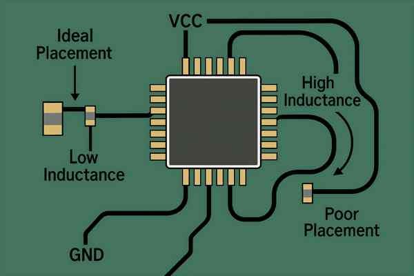
I've learned from years of hands-on board design that neglecting this simple rule is a recipe for headaches later. It can mean the difference between a stable, reliable product and one that fails EMI testing or suffers from random glitches. The high-frequency transient current demanded by a switching IC must be supplied by the local capacitor, not from the distant power supply. Let's dig deeper into the physics and best practices.
How Should a PCB Be Partitioned Into Separate Analog, Digital, and Power Sections?
Worried that your sensitive analog signals are getting corrupted by noisy digital logic? A common mistake is to let these different circuit types bleed into one another, creating a chaotic electrical environment that undermines the performance of your entire system.
Partition your PCB by creating distinct physical zones for analog, digital, and power circuitry. Group related components together within their zone and plan signal flow logically. This strategy minimizes noise coupling by maximizing the physical distance between aggressors and victims.
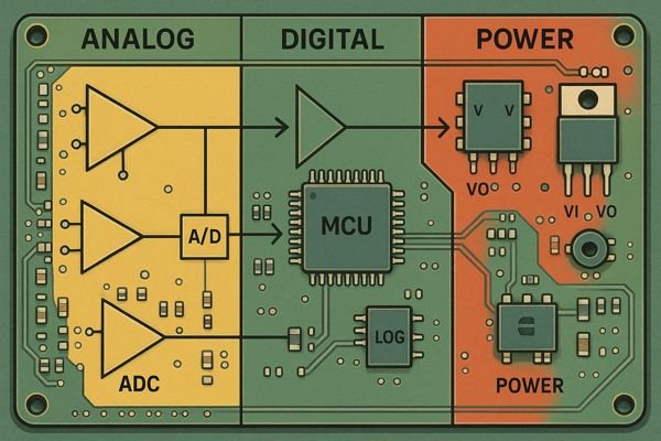
On a mixed-signal medical device I designed, we had a high-precision sensor front-end right next to a microcontroller running a display. Without strict partitioning, the MCU's switching noise coupled directly into the sensor readings, making them useless. By creating dedicated analog and digital sections with a well-defined interface, we isolated the noise and achieved the required 16-bit measurement accuracy.
Planning Your PCB Floorplan: A Deeper Dive
The first step is to create a "floorplan" for your PCB. Before you even place a single component, decide where each functional block will live.
- Identify Functional Blocks: Classify every part of your schematic into functional blocks: sensitive analog (op-amps, sensors), high-speed digital (CPU, FPGA, DDR memory), noisy power (SMPS), quiet power (LDOs), and interface sections (USB, Ethernet).
- Plan the Signal Flow: Arrange these blocks to create a logical, one-way signal flow. A signal should ideally enter the board, move through analog processing, get digitized by an ADC, processed by the digital core, and then sent to an output. This prevents sensitive input signals from looping back near noisy output stages.
- Physical Separation: Noise coupling strength decreases with the square of the distance. Doubling the distance between a noise source and a victim can reduce the coupled noise by 6 dB. A general guideline is to maintain a separation of at least 0.5 inches (12.7 mm) between high-speed digital and sensitive analog sections.
Grounding and Power Plane Strategy
How you handle your ground plane is the most critical decision in partitioning. The debate between a unified and split plane is ongoing, but here’s a practical breakdown.
| Strategy | Description | Best For | Key Risk |
|---|---|---|---|
| Unified Ground Plane | A single, solid ground plane for the entire board. Partitioning is "virtual"—you keep analog and digital components physically separate over their respective areas of the plane. | Most modern mixed-signal designs, especially with high-speed (>50 MHz) digital signals. It provides the lowest impedance return path for digital currents. | Requires disciplined layout. If a digital trace is accidentally routed through the "analog" area of the plane, its return currents will flow there and create noise. |
| Split Ground Planes | The ground plane is physically split into separate analog and digital planes. These are connected at only one point (a "bridge"), typically at the ADC or DAC. | High-precision, low-frequency (<10 MHz) analog systems where keeping even tiny digital ground currents out of the analog section is paramount. | High Risk. If any trace crosses the split, its return path becomes a massive loop, creating a huge antenna that radiates EMI and destroys signal integrity. This is a common failure point. |
Unless you have a very specific, low-frequency, high-sensitivity application, a unified ground plane with careful partitioning is the safer and often better-performing choice for most designs today.
What Placement Techniques Are Used to Isolate Sensitive Analog Components From Noise?
Are you finding that your analog measurements are noisy or inaccurate? Your layout might be letting digital noise creep in and corrupt those sensitive signals, rendering your expensive precision components useless. The key is to reduce both conductive and radiated coupling.
To isolate sensitive analog components, use a multi-layered defense: maximize physical distance from digital noise, shield sensitive traces with guard rings and grounded pours, and provide clean, localized power through LDOs and filtering.
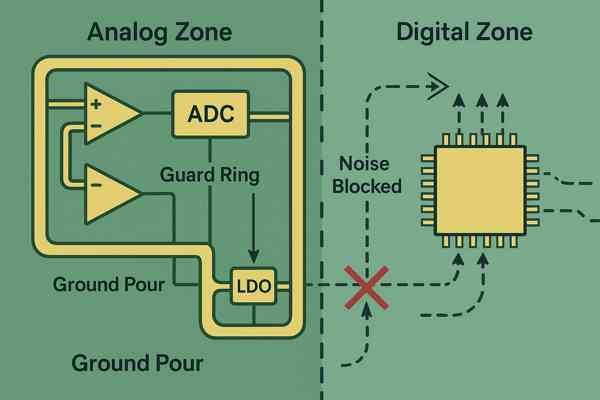
I once worked on a project with a low-level sensor that had a microvolt-level output. The readings were all over the place. We implemented a guard ring around the input traces, tied it to the op-amp's reference voltage, and the noise floor dropped by over 12 dB. This simple layout trick shielded the input from capacitive coupling from a nearby SPI bus.
Analog Isolation Techniques Summary
| Technique | Primary Purpose | Type of Noise Targeted | Best Practice |
|---|---|---|---|
| Physical Distance | Reduce field coupling | Radiated (Capacitive & Inductive) | Place analog circuits >10mm away from high-speed digital or SMPS sections. |
| Guard Ring | Intercept stray electric fields and leakage currents | Capacitive & Conductive | Surround high-impedance traces. Drive the ring with a low-impedance source at the same potential as the signal. |
| Grounded Pour / "Moat" | Create a shield | Radiated (Capacitive) | Surround the entire analog section with a ground pour, stitched to the main ground plane with vias every ~2.5mm. |
| Orthogonal Routing | Minimize trace-to-trace coupling | Capacitive | If analog and digital traces must cross on adjacent layers, ensure they do so at a 90° angle. |
| Stripline Routing | Shield the trace from above and below | Radiated (Capacitive) | Route critical analog signals on an internal PCB layer, between two solid ground planes. |
| Local LDO/Filtering | Prevent noise on power rails | Conductive | Power sensitive analog ICs from a local, clean source like an LDO, not directly from a noisy SMPS rail. |
What Are the Placement Strategies for SMPS Components to Reduce Loop Area and EMI?
Having trouble passing EMC testing? The layout of your switch-mode power supply (SMPS) is likely the culprit. The high-frequency switching currents (high di/dt) in an SMPS create rapidly changing magnetic fields, and according to Faraday's law of induction, this means radiated EMI.
The most critical strategy for SMPS layout is to surgically minimize the area of the high di/dt current loop, often called the "hot loop." This is done by placing the input capacitor, switching MOSFET(s), and freewheeling diode as close to each other as physically possible, using wide copper pours for connections.
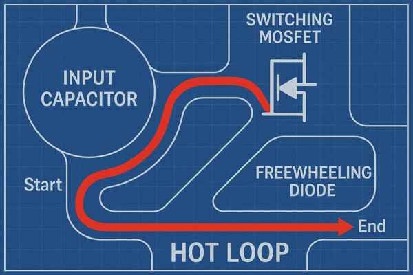
Early in my career, a product I designed kept failing radiated emissions tests between 100-300 MHz. The problem was a buck converter where the input ceramic capacitor was placed an inch away from the switching IC. By moving the capacitor to be directly adjacent to the IC's VIN and PGND pins, we reduced the hot loop area from ~250mm² to under 25mm². The radiated emissions dropped by nearly 20 dB, and the design passed.
SMPS Component Placement Priority (Buck Converter Example)
| Priority | Component | Placement Strategy | The "Why" (Reason) |
|---|---|---|---|
| 1 (Highest) | Input Ceramic Capacitor (C_IN) | Place directly adjacent to the IC's VIN and Power Ground (PGND) pins. | This capacitor supplies the high-frequency switching current. Minimizing its loop path is the #1 factor in reducing EMI. |
| 2 | Switching IC / MOSFETs | Place immediately next to C_IN to complete the "hot loop". | The path from C_IN through the FETs and back to C_IN's ground is the primary high di/dt loop. Every millimeter counts. |
| 3 | Inductor (L) | Place close to the Switch Node (SW) pin of the IC. | Keeps the noisy switch node copper area small. A large SW area is a powerful antenna for radiated noise. |
| 4 | Output Capacitor(s) (C_OUT) | Place close to the inductor and the load. Connect its ground side to a solid ground plane near C_IN's ground. | Ensures a short path for the continuous output current, which improves efficiency and reduces output ripple. |
| 5 (Lowest) | Feedback Network (FB Resistors) | Place close to the IC's FB pin. | Minimizes the chance of noise coupling into the sensitive feedback path, which can cause output voltage instability. Route it away from the SW node. |
How Does Component Placement Affect the Integrity of Power and Ground Planes?
Do you treat your power and ground planes as a magical carpet that solves all your problems? Poor component placement can chop up these planes with vias and cutouts, creating unseen high-inductance paths that degrade performance and cause EMI.
Component placement directly impacts plane integrity by creating discontinuities in the signal return path. Placing dense via fields or components without considering current flow can create splits and slots in planes, forcing return currents into long, convoluted loops, which increases inductance, crosstalk, and EMI.
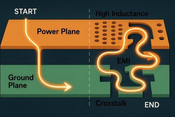
I remember debugging a DDR3 memory interface that was failing timing. The signals looked terrible, with significant overshoot and ringing. The issue was traced to a dense BGA whose via field for inner signals created a "cheese-grater" effect on the ground plane below. High-speed address lines routed over this area had their return paths disrupted, which destroyed their signal integrity.
Common Placement Mistakes vs. Plane Integrity
| Placement Mistake | The Effect on Planes | The Consequence |
|---|---|---|
| Routing a trace over a split plane | The signal's return current is forced to detour around the split. | Creates a massive current loop, resulting in huge radiated EMI and destroyed signal integrity1. |
| Dense via field under a trace (e.g., BGA fanout) | The reference plane becomes a "perforated" surface with high impedance. | The return path is discontinuous, leading to signal reflections, ringing, and crosstalk between adjacent signals. |
| Signal changing layers without a return path via | The return current is stranded on the original layer and must find a distant path (e.g., a decoupling cap) to switch layers. | Creates a large loop, causing ground bounce2 and EMI, particularly for multiple signals switching at once (SSO noise). |
| Placing a noisy component (SMPS) over a quiet ground area | The SMPS's noisy return currents flow through the ground plane intended for sensitive analog circuits. | Conductive noise coupling corrupts the sensitive circuits, defeating the purpose of partitioning. |
What Are the Best Practices for Placement for Good Thermal Management?
Is your board getting unexpectedly hot, or worse, are components failing from overheating? Effective thermal management starts with smart component placement long before you even think about adding a heatsink. A 10°C increase in operating temperature can cut a semiconductor's lifespan in half.
For good thermal management, place high-power components away from board edges to allow for omnidirectional heat spreading, use large copper planes as heatsinks, and implement an array of thermal vias to conduct heat to other layers. Keep temperature-sensitive components far away from these heat sources.
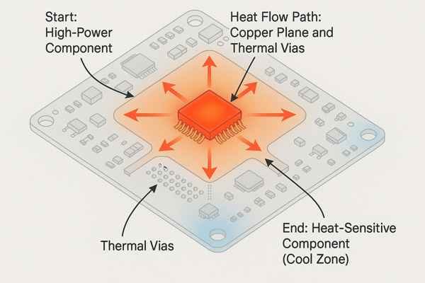
On an industrial controller project, several high-current motor drivers generated over 5W of heat each. Initially, they were clustered near a corner, creating a hot spot that reached 95°C. By redistributing them towards the center and connecting their thermal pads to internal ground planes with 16 thermal vias each, we dropped the peak operating temperature to 72°C, bringing it well within the reliable operating range.
Impact of Placement and Layout on Thermal Resistance
| Technique | Typical Implementation | Estimated Improvement in Thermal Performance |
|---|---|---|
| Component Location | Move a hot component from a board edge to the center. | Reduces component temperature rise by 20-30% due to 360° vs. 180° heat spreading. |
| Copper Pour Area | Connect a thermal pad to a 10cm² copper plane vs. a 1cm² plane. | Can lower thermal resistance (Rth) by >50%. More copper is always better. |
| Copper Weight | Use 2 oz (70µm) copper instead of 1 oz (35µm) copper for planes. | Reduces thermal resistance of the copper plane by nearly 50%. |
| Thermal Vias3 | Add a 4x4 array of 0.3mm vias under a thermal pad. | Can reduce the board-level thermal resistance by 10-15 °C/W, providing a critical path for heat to escape to other layers. |
| Component Separation | Move a sensitive capacitor 20mm away from a 2W power resistor instead of 5mm away. | Can reduce the capacitor's temperature by 10-20°C, dramatically improving its lifespan and stability. |
Conclusion
Component placement is not a game of Tetris. It is a critical engineering discipline that directly dictates your product's performance, reliability, and ability to pass certifications. By thinking about current loops, return paths, and heat flow from the very beginning, you build a foundation for success.
-
Understanding signal integrity is crucial for designing reliable electronic circuits, ensuring minimal interference and optimal performance. ↩
-
Ground bounce can severely affect circuit performance; learning about it helps in designing better systems and avoiding common pitfalls. ↩
-
Explore how thermal vias can significantly enhance heat dissipation in PCBs, improving overall performance and reliability. ↩


