 Skip to content
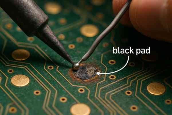
Are you chasing intermittent failures or failed solder joints? This hidden manufacturing defect might be the culprit, turning your reliable design into a ticking time bomb.
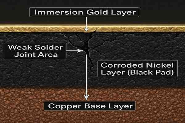
A "black pad" is a critical PCB defect where the nickel layer beneath the immersion gold corrodes during manufacturing. This creates a brittle, non-solderable surface, leading to weak or completely failed solder joints that often appear after thermal stress or during field use.
This problem can be a nightmare for hardware engineers. You can have a perfectly designed schematic and layout, but if the board fabrication process is flawed, you end up with unreliable products. The issue isn't with your design, but with the chemical process used to create the surface finish. Let's dive deeper into what causes this issue and how you can protect your projects from it.
What Causes Black Pad in ENIG PCBs?
Struggling with unexplained solder joint failures on your ENIG boards? The cause might be hidden in the plating chemistry, a problem originating long before your components were placed.
Black pad is caused by excessive corrosion of the electroless nickel layer during the immersion gold plating step. If the gold bath chemistry is too aggressive or improperly controlled, it attacks the nickel underneath, creating a phosphorus-rich, nickel-oxide layer that prevents proper soldering.
In my experience, this is almost always a failure of process control at the PCB fabrication house. The defect isn't random; it's a direct result of a breakdown in the manufacturing chemistry.
How the ENIG Chemical Reaction Fails
The ENIG process uses a displacement (or galvanic) reaction where gold ions in the bath replace nickel atoms on the surface of the pad: 2Au⁺ + Ni → 2Au + Ni²⁺. This should be a self-limiting reaction. However, if the bath chemistry is off, it becomes hyper-corrosive. Instead of just replacing surface atoms, it aggressively attacks the nickel grain boundaries. The corrosion digs deep into the nickel structure, creating fissures that get filled with a brittle nickel-phosphorus oxide.
Common Process Control Lapses That Cause Black Pad
This corrosive attack is typically triggered by poor manufacturing controls. A fabricator must tightly manage these variables:
| Process Variable | Acceptable State | State Leading to Black Pad |
|---|---|---|
| Gold Concentration | Within specified limits | Too high, making the bath overly aggressive. |
| Bath pH Level | Stable and correct | Incorrect pH, which accelerates nickel corrosion. |
| Bath Contaminants | Filtered and pure | Impurities that destabilize the nickel deposit. |
| Immersion Time | Controlled and precise | Too long, allowing excessive time for corrosion. |
Any one of these lapses can initiate the formation of black pad across an entire panel of boards.
What Are the Effects of Black Pad on Solder Joints?
Wondering why your BGAs are cracking or components are lifting off pads? The effects of black pad are catastrophic for long-term reliability, even if they pass initial testing.
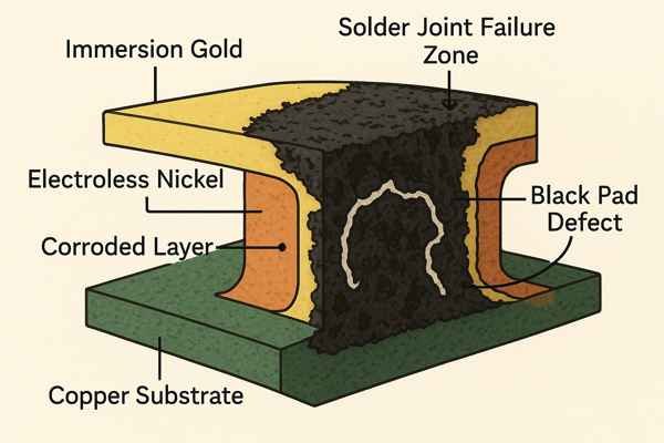
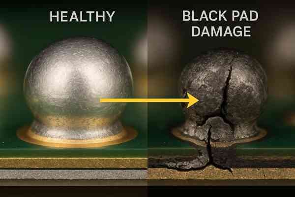
Black pad prevents the formation of a proper intermetallic compound (IMC) between the solder and the nickel layer. This results in an extremely brittle or non-existent connection, leading to cracked joints, open circuits, and catastrophic field failures under thermal or mechanical stress.
The integrity of every solder connection depends on the formation of a good IMC layer. Black pad makes this impossible, fundamentally compromising the joint from the moment it's created.
How Black Pad Prevents a Proper Solder Bond
Think of the IMC as the welded seam that chemically bonds the solder to the pad. A healthy joint forms a strong, uniform Ni₃Sn₄ (nickel-tin) IMC. The black pad layer, which is a mix of nickel oxide and high concentrations of phosphorus, acts as a barrier of crumbly rust. The molten solder can't reach the stable nickel underneath to form this vital chemical bond. You're left with a connection that's just physically sitting on the pad, with no real adhesion.
The Nightmare of Intermittent Field Failures
Initially, a component on a black pad might pass an electrical test at the factory. However, the mechanical bond is virtually non-existent. A slight board flex or a thermal cycle can crack the joint. I once worked on an automotive device that would fail only when the car went over a bump on a cold day. The contraction from the cold and the mechanical shock were just enough to open the cracked joint on a critical sensor. These intermittent faults are the worst-case scenario for an engineer, as they're nearly impossible to replicate and debug.
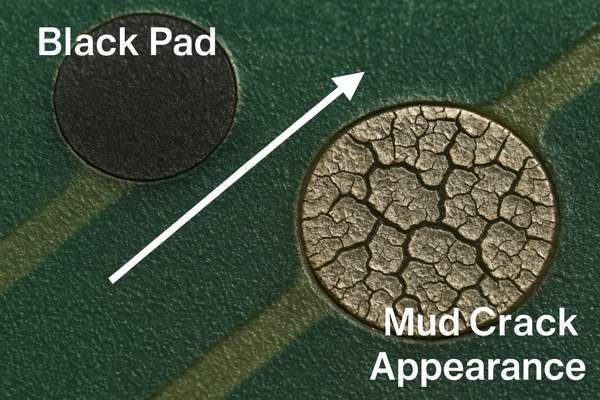
Is There a Difference Between a Black Pad and a "Mud Crack" Appearance?
Have you seen a cracked, dried-mud look on your pads after removing a component? It's a clear warning sign, but it's important to know what you're looking at.
Yes, there is a difference. "Black pad" is the underlying nickel corrosion itself. A "mud crack" appearance is a severe visual manifestation of black pad, where the compromised nickel-phosphorus layer has physically fractured. A pad can have black pad without visible mud cracks.
It's crucial to understand the distinction: one is the disease, and the other is a late-stage, visible symptom.
Distinguishing the Defect from the Symptom
Think of it this way: black pad is the corrosion happening at the nickel grain boundaries. This is often invisible, hidden by the gold layer. The "mud crack" appearance occurs when this corrosion is so severe that the entire nickel deposit loses its structural integrity and fractures, often due to the thermal shock of soldering.
How to Interpret Visual Clues on the Pad
You cannot rely on your eyes to rule out black pad, but you can use them to confirm a severe case.
| Visual Observation | What It Indicates | Reliability Impact |
|---|---|---|
| Pad looks normal/gold | Could still have hidden black pad. | Unknown |
| Pad looks dark/black | Indicates severe corrosion; this is classic "black pad." | Catastrophic |
| Pad shows mud cracks | Complete fracture of the nickel layer; an advanced defect. | Catastrophic |
If you see mud cracks, it's not just one bad pad. It’s an indictment of the entire batch's manufacturing process.
How Do You Identify or Test for Black Pad?
How can you be certain that black pad is the root cause of your failures? Guessing isn't an option when reliability is on the line; you need definitive proof.
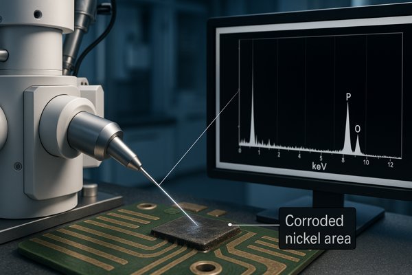
The most reliable method for identifying black pad is using a Scanning Electron Microscope (SEM) with Energy-Dispersive X-ray (EDX) analysis. This allows you to see the corroded nickel structure and confirm its elemental composition, specifically detecting high levels of phosphorus and oxygen.
When I suspect a black pad issue, we move immediately to formal failure analysis. There's a clear process for getting an undeniable result.
Preliminary Tests That Suggest Black Pad
Simple mechanical tests can provide the first clues. A solder ball shear test on a BGA or a pull test on a discrete component will show significantly lower force-to-failure values than expected. The joint will break cleanly at the pad interface, often taking no metal with it. This is a strong indicator.
Definitive Lab Analysis: SEM/EDX Confirmation
For conclusive proof, we send samples to a lab.
- Cross-Section: The failed joint is cut vertically and polished. This allows microscopic inspection of the boundary layer between the solder and the pad.
- SEM Imaging: The cross-section is placed in a Scanning Electron Microscope. At high magnification (e.g., 5000x), the fractured, crystalline structure of the corroded nickel becomes visible.
- EDX Spectrum: The EDX detector analyzes the elemental composition at the fracture line. A black pad defect is confirmed by finding high signal peaks for Oxygen (O) and Phosphorus (P) right where the nickel should be.
This data is the "smoking gun" that proves black pad is the cause.
What Are the IPC Standards Related to Black Pad and ENIG Quality?
How do you specify ENIG correctly to protect yourself? You need to rely on industry standards to define quality and hold your suppliers accountable for their process.
The primary standard is IPC-4552B (released in 2021), Specification for Electroless Nickel/Immersion Gold (ENIG) Plating for Printed Boards. This standard refines thickness requirements and process controls to better prevent defects like black pad.
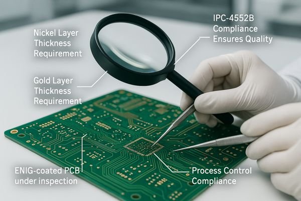
When I send out a design for fabrication, I explicitly call out compliance with the latest standard, IPC-4552B1, on my fab notes. The "B" revision is important as it addresses the process more rigorously.
The Engineering Purpose Behind IPC-4552B Specs
The specifications in the standard are not arbitrary; they are designed to balance protection, solderability, and cost.
- Nickel (3-6 µm): Needs to be thick enough to be a robust barrier against copper migration, but not so thick that it creates excessive stress.
- Gold (min 0.05 µm): Must be thick enough to cover the nickel completely and prevent any oxidation during storage, but thin enough that it completely dissolves into the solder joint. Too much gold (
>0.1 µm) can cause gold-tin embrittlement, which is another failure mode.
Key Plating Parameters Mandated by IPC-4552B
The standard specifies the composition and thickness of the plating to ensure a robust, solderable surface.
| Plating Parameter | IPC-4552B Specification | Engineering Rationale |
|---|---|---|
| Nickel Thickness | 3 to 6 µm (118.1 to 236.2 µin) | Provides a solderable, durable barrier over the copper. |
| Gold Thickness | 0.05 µm minimum (2.0 µin) at 4 sigma below the mean | Protects nickel from oxidation without causing embrittlement. |
| Phosphorus Content | 7% to 11% by weight in the nickel deposit | Tighter range for optimal corrosion resistance and solderability. |
Note that the phosphorus content range was tightened in revision B to guide manufacturers toward the "sweet spot" for reliability.
How Can Black Pad Be Prevented During the PCB Manufacturing Process?
Tired of reacting to failures? The best strategy is to prevent black pad from ever forming by choosing the right manufacturing partner and understanding their process.
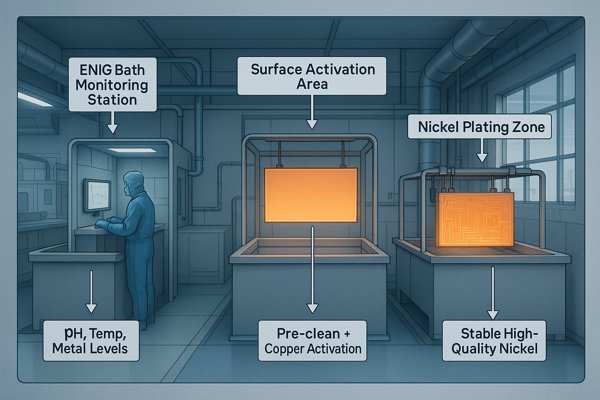
Black pad is prevented through rigorous process control at the PCB fabrication house. This includes tight management of the ENIG bath chemistry (pH, temperature, metal concentration), ensuring proper pre-cleaning and activation of copper surfaces, and using a high-quality, stable nickel bath.
As a design engineer, your power lies in selecting a vendor who can demonstrate this control.
How to Vet a Fabricator's ENIG Process
Don't just choose the cheapest supplier. Ask potential partners direct questions about their process. A good fabricator will be able to provide data, not just promises.
A Checklist for Critical Process Variables
Here is a checklist of what a high-quality fabricator should be monitoring for their ENIG line:
- [ ] Automated chemical dosing and monitoring for the nickel and gold baths.
- [ ] Regular analysis and control of the phosphorus content in the nickel bath.
- [ ] Strict control over immersion times and bath temperatures.
- [ ] Multi-stage cleaning and micro-etching processes prior to plating.
- [ ] Regular carbon treatment of baths to remove organic contaminants.
The Importance of Documentation and Traceability
Always request a certificate of conformance (CoC) with your order that explicitly states compliance with IPC-4552B. For critical projects, ask for the actual process control records (e.g., XRF thickness measurements, bath analysis logs) for your specific production lot.
What Is the Role of Phosphorus Content in the Nickel Bath for ENIG?
You might think all nickel is the same, but for ENIG, a single element makes all the difference between a reliable board and a defective one.
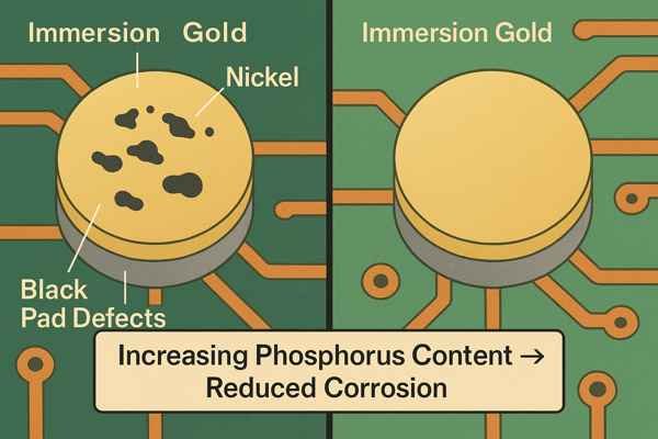
The phosphorus content in the electroless nickel bath is critical for preventing black pad. A higher phosphorus content (typically 7-11%) makes the nickel deposit amorphous and more chemically resistant to corrosion from the immersion gold bath, significantly reducing the risk of black pad.
The phosphorus isn't just an impurity; it's a deliberate alloy that defines the nickel's properties.
How Phosphorus Content Affects Nickel's Structure
The percentage of phosphorus co-deposited with the nickel determines its microstructure, which in turn dictates its corrosion resistance.
| Phosphorus Content | Nickel's Microstructure | Black Pad Risk |
|---|---|---|
| Low (1-4%) | Crystalline | High. Prone to corrosion along grain boundaries. |
| Mid (5-9%) | Mixed/Amorphous | Moderate. A compromise of solderability and resistance. |
| High (10-13%) | Fully Amorphous | Low. Lacks grain boundaries, making it highly corrosion-resistant. |
The IPC Standard and Best Engineering Practice
The latest standard, IPC-4552B, recommends a tighter range of 7-11% phosphorus content. This reflects a consensus in the industry that this range provides the best balance of corrosion resistance and good solderability. A vendor who cannot tell you their target phosphorus content and control range is a major red flag.
Can a PCB With Black Pad Be Reworked or Repaired?
Have you discovered a batch of expensive boards has black pad? The immediate question is whether you can salvage them, but the answer is often a hard one to swallow.
No, a PCB with a black pad defect cannot be reliably reworked or repaired. The defect is integral to the surface finish itself. The corroded nickel layer under the gold cannot be fixed, and any attempt to solder onto it will result in a weak, unreliable joint.
This is one of those situations in engineering where there is no easy fix. Trying to "save" the boards is a dangerous gamble.
Why Repair and Rework Attempts Fail
The problem is not on the surface; it's the foundation of the pad itself. You cannot scrape, clean, or chemically treat the corroded nickel layer away without destroying the pad. Any solder applied will be bonding to a crumbly, oxidized layer, not the stable nickel required for a proper intermetallic connection.
The Financial Calculation: Scrapping Boards vs. Field Recalls
I was once on a project where a manager, desperate to save costs, pushed to use a batch of boards we suspected had black pad. The argument was that the cost of scrapping them ($20,000) was too high. They passed initial tests. Six months later, the field failure recall cost over $2,000,000 and did immense damage to the company's reputation. The math is simple:
| Decision Option | Immediate Financial Cost | Long-Term Financial & Brand Risk |
|---|---|---|
| Scrap Boards | High (Cost of boards) | Zero. Problem is eliminated. |
| Use Boards | Zero | Extremely High. Cost of failures, recalls, liability. |
The Only Responsible Engineering Action
If black pad is confirmed, the only correct engineering decision is to quarantine and scrap the entire lot. It's a painful but necessary step to protect your product and your customers.
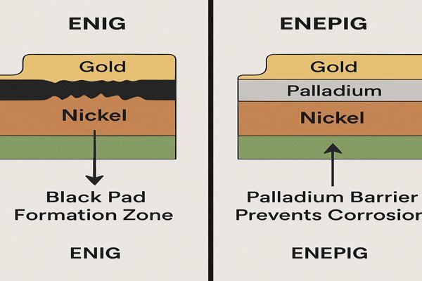
What Is the Difference Between ENIG and ENEPIG?
You've heard of ENIG, but now you see ENEPIG quoted as an option. Is it just another acronym, or is it a fundamentally different and better surface finish?
The key difference is an extra layer of protection. ENEPIG (Electroless Nickel, Electroless Palladium, Immersion Gold) adds a layer of palladium between the nickel and the gold. ENIG is just Electroless Nickel, Immersion Gold. This palladium layer is the game-changer.
To understand the impact, let's compare the layer structures directly.
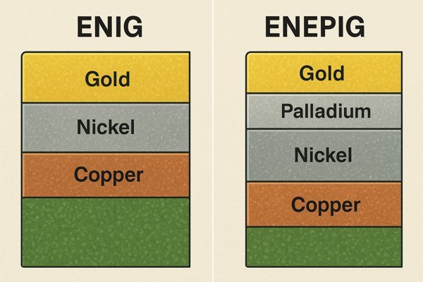
The Layer Structure of ENIG
The ENIG process is a two-step plating process over the base copper pad.
- Electroless Nickel (Ni): A 3-6 µm layer that acts as a barrier to prevent copper migration and provides the solderable surface.
- Immersion Gold (Au): A very thin (0.05-0.1 µm) layer to protect the nickel from oxidation.
The weakness here is that the gold deposition process can directly attack the nickel.
The Layer Structure of ENEPIG
ENEPIG adds a crucial intermediate step, making it a three-layer system.
- Electroless Nickel (Ni): The same 3-6 µm foundation layer.
- Electroless Palladium (Pd): A 0.05-0.15 µm layer that is deposited on top of the nickel.
- Immersion Gold (Au): A thin final layer.
The palladium completely covers the nickel, protecting it from the aggressive immersion gold chemistry. This eliminates the root cause of black pad.
Is ENEPIG a Solution to the Black Pad Problem?
After learning about the risks of black pad with ENIG, you need a reliable alternative. Is ENEPIG the definitive solution you've been looking for?
Yes, absolutely. ENEPIG is widely considered the ultimate solution to the black pad problem. The addition of the electroless palladium layer acts as a barrier, preventing the immersion gold from corroding the nickel layer, thus eliminating the mechanism that creates black pad.
ENEPIG was developed specifically to overcome the inherent weakness of the ENIG process.
How the Palladium Layer Prevents Black Pad
The palladium layer is the key innovation. It is chemically noble and acts as a robust barrier, isolating the sensitive nickel layer from the immersion gold bath. The gold now deposits onto the palladium, not the nickel, preventing any possibility of nickel corrosion. This simple addition completely engineers the black pad problem out of the process.
Additional Engineering Benefits of ENEPIG
Beyond preventing black pad, ENEPIG offers other advantages, earning it the nickname "the universal finish."
| Feature | Engineering Benefit |
|---|---|
| Black Pad Immunity | Eliminates the primary failure mode of ENIG. |
| Wire Bondable | Supports both gold and aluminum wire bonding. |
| Excellent Solderability | Provides a highly reliable solder joint. |
| Long Shelf Life | Stable for over 12 months. |
Balancing the Cost vs. Risk of ENEPIG
The main drawback of ENEPIG is its higher cost due to the precious metal palladium. However, for high-reliability applications, complex assemblies, or boards with expensive components like FPGAs and processors, the extra cost is a small price to pay for what is essentially insurance against catastrophic failure.
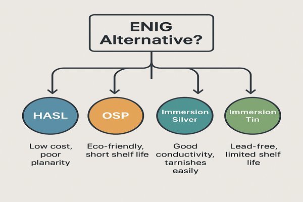
What Are the Best Alternative Surface Finishes to ENIG?
If you're wary of ENIG and ENEPIG is too costly for your project, what other options do you have? Choosing the right finish is a trade-off between cost, performance, and process complexity.
The best alternatives to ENIG are HASL, OSP, Immersion Silver, and Immersion Tin. Each has distinct advantages and disadvantages in terms of cost, shelf life, planarity, and suitability for different components. The choice depends entirely on your specific application requirements.
There is no single "best" finish. The right choice is an engineering trade-off.
A Decision Matrix for Selecting a Surface Finish
When selecting a finish, I mentally run through these questions:
- Fine-Pitch Components? If yes (BGA, 0.4mm pitch QFN), I need a planar finish. HASL is out.
- Long Shelf Life / Multiple Assembly Stages? If yes, OSP is risky. ENIG, ENEPIG, or ImAg are better.
- High-Frequency Signals? If yes, the smooth surface of ImAg, ENIG, or ENEPIG is preferable to minimize skin effect losses.
- Cost Sensitivity? If it's a high-volume, low-cost consumer product, OSP or HASL (if components allow) are the top contenders.
- Reliability Critical? For medical, aerospace, or automotive, the risk of black pad makes ENEPIG the safest choice, despite the cost.
Comparing the Top Alternative Finishes
| Surface Finish | Planarity | Shelf Life | Relative Cost | Best For... | Not For... |
|---|---|---|---|---|---|
| HASL (Leaded/LF) | Poor | > 12 mos | Low | Simple, robust boards; through-hole; large-pitch SMT. | Fine-pitch components; BGAs; planarity needs. |
| OSP (Organic) | Excellent | < 6 mos | Very Low | High-volume consumer goods; fast assembly timeline. | Long-term storage; multiple reflow cycles. |
| Immersion Silver | Excellent | ~6 mos | Medium | RF/High-speed circuits; press-fit; fine-pitch. | Environments with sulfur; long-term storage. |
| Immersion Tin | Good | ~6 mos | Medium | Press-fit connectors; backplanes; some automotive. | Designs where tin whiskers are a critical risk. |
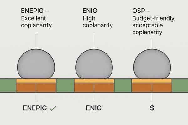
What Are the Best PCB Surface Finishes for BGA Components?
Using Ball Grid Arrays (BGAs)? The wrong surface finish can ruin your assembly yield and long-term reliability. Coplanarity is king, and not all finishes are created equal.
The best surface finishes for BGAs are ENEPIG and properly processed ENIG. Both provide the exceptionally flat (planar) surface required for all the solder balls on a BGA to make reliable contact with the pads during reflow. OSP is a viable low-cost alternative.
With BGAs, the microscopic flatness of the pads across the entire footprint is not negotiable.
Why Surface Planarity is Critical for BGAs
A BGA has a grid of solder balls that all must melt and fuse to their pads. If the PCB pads are not perfectly flat (non-coplanar), you get catastrophic assembly defects. The most common is "head-in-pillow2," where the solder paste on the pad and the BGA ball both melt but fail to coalesce into a single joint, creating an open circuit that is nearly impossible to inspect visually. Excellent planarity is the number one defense against this.
A Ranking of BGA-Compatible Finishes
Your choice of finish should prioritize planarity and reliability.
| Rank | Finish | Planarity | Reliability for BGAs | Primary Use Case |
|---|---|---|---|---|
| 1 | ENEPIG | Excellent | Highest. Immune to black pad. | High-reliability, high-cost, or high-density BGA applications. |
| 2 | ENIG | Excellent | High. Excellent planarity, but requires a trusted vendor. | Mainstream applications where process control is guaranteed. |
| 3 | OSP | Excellent | Good. Excellent planarity, but limited shelf life. | High-volume, cost-sensitive assembly with a tight timeline. |
Which Surface Finish to Absolutely Avoid for BGAs
HASL (Hot Air Solder Leveling) is completely unsuitable for any modern BGA. The process creates an uneven, domed surface on each pad, making it impossible to guarantee that all solder balls will make a reliable connection. Using HASL with BGAs is a recipe for very low assembly yields and field failures.
Conclusion
Black pad is a critical manufacturing defect in ENIG boards caused by poor process control. Understanding its causes, effects, and prevention methods, like choosing a quality vendor or using ENEPIG, is essential for reliable electronics.


