 Skip to content
Struggling with intermittent signal integrity issues or failing EMC tests? You might be overlooking the most critical part of your PCB layout: the return path. Many engineers focus only on the signal trace, forgetting that current travels in a loop, leading to costly redesigns and project delays. The solution is to understand that a solid ground plane is the essential, low-impedance highway for your signal's return current.
A ground plane is a large, continuous area of copper on a PCB connected to the circuit's ground reference. For high-speed signals, it's not just a 'zero-volt' reference; it's the primary return path for current. A well-designed ground plane provides a low-impedance path, minimizing signal degradation and EMI.
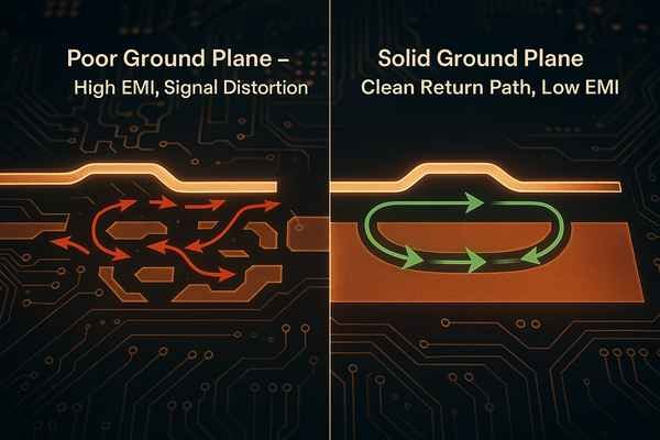
As an engineer with nearly 20 years of experience, I've seen countless projects succeed or fail based on how the ground plane and return paths were managed. At high frequencies, the principles of DC circuits no longer apply. The return current doesn't take the path of least resistance; it takes the path of least impedance. Think of it like a lightning strike—it seeks the easiest path to ground, which is determined by inductance, not just resistance. For a high-frequency signal, the path of least impedance is directly underneath the signal trace. This is due to a physics principle called mutual inductance1, which tightly couples the signal and its returning current. When we fail to provide this direct path, we're inviting problems like crosstalk, reflections, and radiated emissions. This understanding is fundamental, something I learned the hard way while designing complex products at companies like Honeywell and Smiths Medical. A solid ground plane is your first and best defense against a host of high-speed design headaches.
How should a return path be designed for a signal that crosses layers on a PCB?
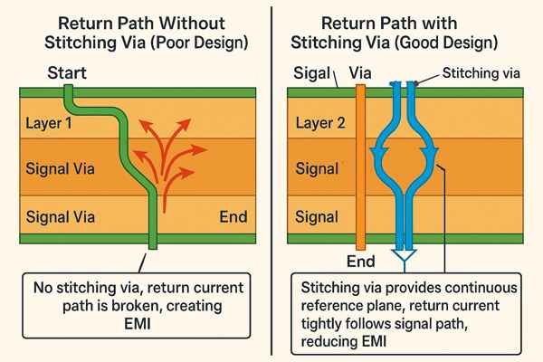
You've carefully routed a high-speed signal, but now you need to switch layers. If you just drop a via and continue, you might have unknowingly created a massive antenna. This simple oversight can radiate enough noise to doom your product's EMC certification, forcing expensive and time-consuming fixes. The solution is to provide a dedicated, low-impedance path for the return current to follow the signal.
When a signal changes layers, its reference plane might also change. You must provide a clear, low-impedance path for the return current to follow the signal. This is typically done by placing a "stitching" via next to the signal via, connecting the two reference planes.
Technical Breakdown of Cross-Layer Return Paths
When a high-speed signal transitions between layers, its return current must follow. The specific solution depends on whether the reference planes are the same potential (e.g., GND to GND) or different potentials (e.g., GND to VCC). Each scenario requires a different approach to ensure a low-impedance path.
| Transition Type | Problem | Solution | Key Component(s) |
|---|---|---|---|
| Ground to Ground | The return current on the first ground plane is physically separated from the second ground plane. | Provide a direct, low-inductance connection between the two ground planes. | A ground stitching via placed as close as possible to the signal via. |
| Ground to Power | The return current cannot flow directly from a ground plane to a power plane. | Provide a high-frequency AC path for the current to jump between planes. | A small decoupling capacitor2 (e.g., 1-10 nF, 0402 package) placed next to the signal via. |
To solve this, we place a ground stitching via as close as physically possible to the signal via for a ground-to-ground transition. According to IPC-2221A, standard via-to-via clearance is often around 0.5 mm (20 mils), but you should get it as tight as your fabrication process allows. If the signal's reference changes from a ground plane to a power plane, a stitching via alone won't work. In this case, you must place a small decoupling capacitor (e.g., a 10 nF, 0402-size X7R or C0G/NP0 ceramic capacitor) very close to the signal via. The small package size is crucial to minimize the capacitor's own parasitic inductance, ensuring it provides an effective high-frequency bridge between the planes.
What are stitching vias and when should they be used?
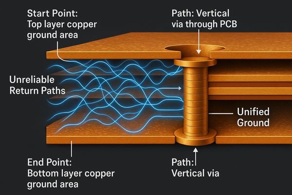
Your design has multiple ground areas, but are they truly connected at high frequencies? Simply pouring copper on different layers and calling it "ground" isn't enough. Without proper connections, you create isolated ground islands that cause unpredictable return paths, making your circuit's behavior unreliable and hard to debug. The solution is to use stitching vias to effectively tie these ground areas together.
Stitching vias are vias that connect different ground planes or large ground pours on a PCB. They should be used whenever you need to ensure two or more ground areas behave as a single, continuous ground plane, especially around high-speed traces or along the board edge for EMI shielding.
Practical Insights on Using Stitching Vias
Stitching vias essentially "sew" together different copper ground regions, lowering the impedance between them. The spacing rule of thumb, \(\lambda/20\), works because it ensures any gaps or "holes" in the ground network are electrically small compared to the wavelength of the signals you are concerned about, preventing fields from leaking or radiating through them.
It's also important to remember that vias are not perfect conductors; they have their own parasitic inductance, typically in the range of 0.3 nH to 1.0 nH depending on their length and diameter. For extremely critical nets or when stitching a low-impedance power plane, a single via's inductance can be too high. In these cases, using a cluster of two, three, or even four stitching vias in parallel is a common technique. Just as with resistors in parallel, the total inductance of the parallel vias is significantly lower than that of a single via, providing a much more effective, low-impedance connection between planes. This is especially critical when providing a return path for high-current or very high-frequency signals.
| Application | Recommended Stitching Via Spacing | Rationale |
|---|---|---|
| Board Edge EMI Shielding | \(\le \lambda/20\) | Creates a Faraday-like cage to contain EMI. Prevents radiation from board edges. |
| Around High-Speed Traces | \(\le \lambda/8\) to \(\lambda/20\) | Ensures a continuous, low-inductance return path adjacent to the signal. |
| Guard Trace Stitching | \(\le \lambda/8\) | Connects the guard trace to the main ground plane, making it effective. |
| Ground Pour Stitching | Grid pattern, every 1-2 cm | Lowers overall ground impedance and prevents ground islands from forming. |
What are the considerations for using a solid ground plane versus a split ground plane?
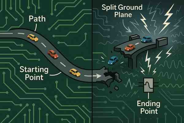
You're designing a mixed-signal board with noisy digital circuits and sensitive analog components. The classic advice is to split the ground plane to isolate them. But this is one of the most misunderstood and dangerous techniques in PCB layout; one wrong trace crossing that split can create a massive antenna, destroying your EMI performance. The solution is to use a solid ground plane and practice intelligent component partitioning.
A solid ground plane is almost always the best choice for any design with high-speed digital signals. Split ground planes create more problems than they solve, such as creating large return path loops for signals that must cross the split, leading to massive EMI.
Why the Choice Between Solid and Split Planes Matters
The choice between a solid and split ground plane fundamentally impacts return path integrity and EMI. A solid plane provides an unbroken "image" plane for return currents, while a split plane deliberately breaks it. The table below summarizes the key differences.
| Feature | Solid Ground Plane | Split Ground Plane |
|---|---|---|
| Return Path Control | Excellent. Current naturally follows the path of least impedance under the signal trace. | Poor. Any trace crossing the split creates a huge, uncontrolled return loop. |
| EMI Performance | Superior. Minimized loop areas lead to low radiation. | High Risk. Large current loops act as efficient antennas, causing high EMI. |
| Mixed-Signal Isolation | Achieved by partitioning the layout into analog and digital sections. | Achieved by creating a physical "moat" or gap in the copper. |
| Design Complexity / Risk | Low. It is a forgiving and robust design practice. | Very High. Extremely easy to make a critical mistake that ruins board performance. |
A far better approach, as advocated by experts like Henry Ott, is to use a solid ground plane and partition your layout. Think of your PCB as a piece of real estate. You place the noisy digital components in one "neighborhood" and the sensitive analog components in another. Route all their respective traces within their own neighborhoods. The high-frequency digital return currents, following their image paths, will stay confined under the digital traces, naturally remaining within the digital section. This achieves the desired isolation without the catastrophic risk of a split plane.
How are return paths for differential pairs managed?
Differential pairs seem magical with their high-speed capabilities and noise rejection. This leads many engineers to think the return current just flows back on the other trace. Ignoring the reference plane is a critical mistake that can compromise impedance control and create common-mode noise, negating the benefits of using a differential pair in the first place. The solution is to remember that the pair as a whole still needs a solid reference plane.
While the primary return current of one trace in a differential pair is the other trace, the pair as a whole is still referenced to a ground or power plane. This reference plane is crucial for maintaining the pair's characteristic impedance and minimizing common-mode noise.
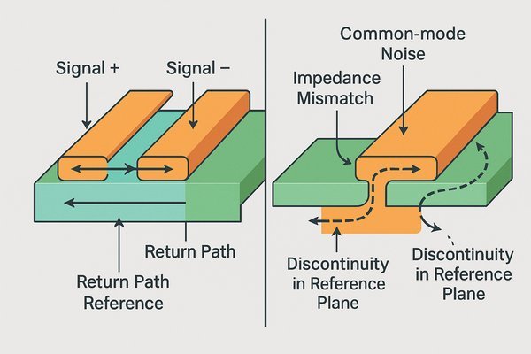
A Closer Look at Differential Pair Return Paths
Maintaining the balance of a differential pair is paramount. Any asymmetry in the layout can convert the desired differential signal into a common-mode signal3, which radiates noise. Adhering to strict layout rules is critical.
| Best Practice (Do) | Common Mistake (Don't) |
|---|---|
| Route pairs tightly coupled and at a constant distance. | Allow the spacing between traces to vary along the route. |
| Route pairs over a solid, continuous reference plane. | Route pairs over gaps, splits, or different reference planes. |
| Keep the lengths of the two traces precisely matched. | Allow for significant length differences between P and N traces. |
| Use symmetrical entry/exit from pads and vias. | Route one trace with sharp bends while the other is straight. |
| Use stitching vias for the return path on layer changes. | Forget to provide a return path via when changing layers. |
When you see high mode conversion (e.g., \(S_{cd21}\)) in a simulation, it's almost always due to a breakdown in one of these rules, most often related to the reference plane. Engineers sometimes try to fix this with a common-mode choke. While these chokes can be effective, they are often a "band-aid" for a layout problem. A well-laid-out differential pair with a solid, continuous reference plane should be inherently balanced and may not need a choke at all.
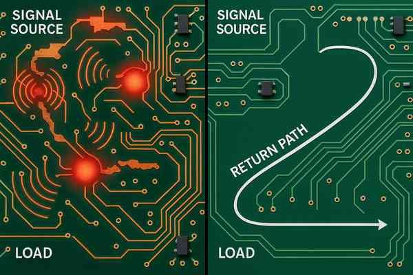
What are the best PCB layout techniques to minimize return path loops?
You followed all the rules for component selection and schematic design, but your prototype is failing. The culprit is often hidden in the layout: large return path loops that you can't see, which act as antennas creating noise, crosstalk, and causing you to fail EMI testing. To eliminate these loops, you must adopt a disciplined layout approach focused on providing a direct, uninterrupted return path for every critical signal.
The most effective technique is to use a solid, uninterrupted ground plane as your primary reference layer. Beyond that, ensure every high-speed signal trace is routed as close as possible to its return path, avoiding any gaps or splits in the reference plane.
From My Experience: The True Cost of a 2-Layer Board
Minimizing loop area is the cardinal rule of high-speed layout. I've often seen junior engineers try to save money by using a 2-layer board for a design with a high-speed microcontroller or interface. This is almost always a false economy. On a 2-layer board, the bottom layer must serve as both the ground plane and a routing layer. The ground plane is inevitably chopped into pieces by traces, creating a "minefield" of slots and unpredictable return paths.
The headaches and hours of debugging spent trying to fix the resulting signal integrity and EMI problems far outweigh the small cost savings. My strong recommendation is that for any design involving signals faster than a few megahertz, a 4-layer board should be the starting point. It's the single best investment you can make for a successful design.
| Good Practice | Bad Practice | Impact of Bad Practice |
|---|---|---|
| Use a 4+ layer board with solid reference planes. | Use a 2-layer board with a heavily routed ground layer. | High ground impedance, unpredictable return paths. |
| Place stitching via next to signal via when changing layers. | Change layers without a return path via. | Discontinuous return path, signal reflection, EMI. |
| Route high-speed signal over solid ground plane. | Route signal over a split or gap in the ground plane. | Large loop area, high inductance, massive EMI. |
| Keep return path physically close to the signal trace. | Let return path meander across the board. | Increased loop inductance and noise susceptibility. |
How is the inductance of a return path calculated?
You know that minimizing loop area is key for a low-inductance return path. But without a way to quantify it, you're just guessing. This can lead to over-engineering or, worse, under-engineering your design, resulting in signal integrity problems that are only discovered after manufacturing. The solution is to use established formulas to estimate the loop inductance, which helps you make better design trade-offs.
The inductance of a return path is not calculated in isolation; you calculate the total loop inductance of the signal and its return. For a microstrip trace over a ground plane, this inductance is primarily a function of the height of the trace above the plane and its length.
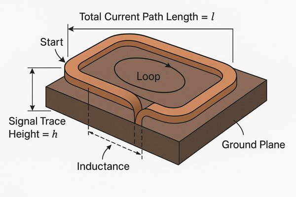
The Engineering Details of Loop Inductance Calculation
For a designer, thinking in terms of the total loop area is what matters. The physical parameters of your trace and stackup directly influence this loop inductance.
| Parameter Change | Effect on Loop Inductance (\(L_{loop}\)) | Reason |
|---|---|---|
| Increase trace height (\(h\)) above plane | Increases \(L_{loop}\) | Increases the cross-sectional area of the current loop. |
| Decrease trace height (\(h\)) above plane | Decreases \(L_{loop}\) | Decreases the cross-sectional area of the current loop. |
| Increase trace width (\(w\)) | Decreases \(L_{loop}\) | Spreads current over a wider area, reducing current density and inductance. |
| Increase trace length | Increases total \(L\) | Inductance scales linearly with the length of the conductor path. |
Let's see what happens when that path is interrupted. Imagine a signal with a fast rise time of 100 ps needs to cross a 0.5-inch gap in the ground plane. The new, larger loop might add 10 nH of inductance. If the signal is driving 50 mA of current, we can estimate the voltage disturbance (\(V\)) using the formula \(V = L \frac{di}{dt}\). Here, \(\frac{di}{dt}\) is roughly \(50 \text{ mA} / 100 \text{ ps} = 5 \times 10^8 \text{ A/s}\). The induced voltage glitch would be \(V = (10 \times 10^{-9} \text{ H}) \times (5 \times 10^8 \text{ A/s}) = 5 \text{ V}\). This is a catastrophic glitch that would completely disrupt the signal.
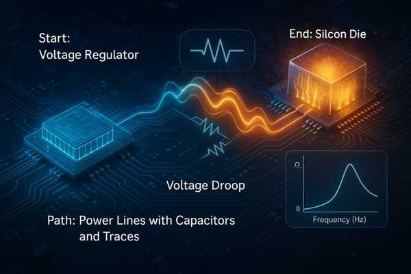
What is Power Distribution Network (PDN) impedance analysis?
Your high-speed processor or FPGA keeps crashing randomly, even though your logic seems perfect. You've checked the code and the signals, but the real issue might be "starvation"—your power supply isn't clean enough, causing voltage droops that lead to unpredictable and frustrating system failures. The solution is PDN analysis, a method to guarantee your power delivery system is robust enough for the job.
Power Distribution Network (PDN) impedance analysis is the process of ensuring that the entire power delivery system—from the voltage regulator to the IC's silicon die—has a sufficiently low impedance across a wide frequency range to meet the transient current demands of the ICs.
Under the Hood of PDN Capacitor Strategy
A good PDN strategy involves selecting a range of capacitor values to cover the entire frequency spectrum. Each capacitor type is chosen for its effectiveness in a specific frequency band, determined by its value and parasitic properties (ESR, ESL).
| Capacitor Type / Role | Typical Value Range | Effective Frequency Range | Typical Placement Location |
|---|---|---|---|
| Bulk Decoupling | \(10 \mu F - 1000 \mu F\) | DC - 500 kHz | Near the Voltage Regulator Module (VRM) |
| Mid-Frequency Decoupling | \(0.1 \mu F - 10 \mu F\) | 500 kHz - 20 MHz | Distributed around the PCB, near IC groups |
| High-Frequency Decoupling | \(1 nF - 100 nF\) | 20 MHz - 500+ MHz | As close as possible to IC power pins |
| On-Die / Package | pF - nF | \(> 500 \text{ MHz}\) | Inside the IC package or on the silicon die |
The goal is to choose values whose effective ranges overlap, creating a smooth, continuous low-impedance path for current at any frequency. The target impedance (\(Z_{target}\)) is calculated as \(Z_{target} = \frac{\Delta V}{\Delta I}\). For a 1.2V core that can tolerate 5% noise (60 mV) with a 10A transient, the target is \(Z_{target} = \frac{0.060 \text{ V}}{10 \text{ A}} = 6 \text{ m}\Omega\). PDN simulation tools are critical for visualizing this combined impedance profile and ensuring there are no dangerous high-impedance peaks where the impedance of one capacitor starts to rise before the next one takes over.
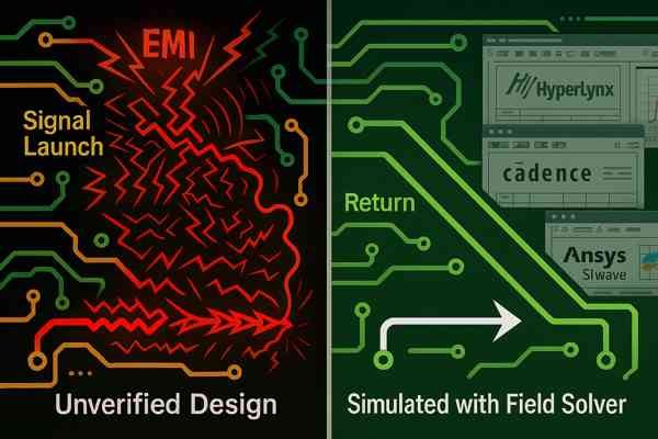
What software tools are available to simulate or analyze signal return paths?
You understand the theory of return paths, but how can you be certain your layout is correct before spending thousands on prototypes? Guessing is not a strategy. Going to fabrication with an unverified design is a huge financial risk and can lead to major project delays if a layout flaw forces a board re-spin. The solution is to use specialized software that lets you see and fix these invisible problems before they become physical.
Several powerful software tools, known as field solvers, can simulate and analyze signal return paths. These tools help you visualize current flow, predict signal integrity issues, and analyze EMI before fabrication. Key players include HyperLynx, Cadence Sigrity, and Ansys SIwave.
In-Depth Analysis of Return Path Simulation Tools
Choosing the right tool depends on your specific needs, from pre-layout analysis to post-layout verification and EMI troubleshooting. Here’s a quick comparison of some industry-standard options.
| Tool Name | Developer | Typical Use Case | Key Feature |
|---|---|---|---|
| HyperLynx SI/PI4 | Siemens EDA | Pre- and post-layout SI/PI analysis for most designs. | Tightly integrated with many PCB tools (e.g., Altium, Xpedition). User-friendly. |
| Cadence Sigrity5 | Cadence | High-performance systems (servers, networking). | Hybrid solver for high accuracy and speed. Excels at complex PDN analysis. |
| Ansys SIwave6 | Ansys | EMI/EMC analysis and complex 3D field problems. | Full-wave 3D electromagnetic solver for maximum accuracy. |
| Keysight ADS | Keysight | RF and Microwave circuit design and simulation. | Comprehensive tool for high-frequency applications, including Momentum 3D solver. |
To get meaningful results, you must provide the simulator with accurate information. This includes precise stackup data from your fabricator (dielectric constant, \(\epsilon_{r}\), and loss tangent, \(\tan\delta\), at frequency) and high-quality models for all components (IBIS for drivers, S-parameters for connectors). Running a simulation with generic models will give you a generic, and likely incorrect, answer.
Conclusion
Mastering the return path is not just an advanced topic; it's the foundation of modern electronics design. A solid ground plane and disciplined layout are your best tools for ensuring signal integrity and passing EMC.
-
Learning about mutual inductance can enhance your understanding of signal integrity and improve your high-frequency design skills. ↩
-
Decoupling capacitors are vital for maintaining power integrity in circuits; learn how they function and their applications. ↩
-
Learning about common-mode signals can help you troubleshoot and improve circuit performance. Check out this informative link. ↩
-
Explore the features of HyperLynx SI/PI to understand how it can enhance your PCB design process with its user-friendly interface and integration capabilities. ↩
-
Discover how Cadence Sigrity's hybrid solver can optimize your high-performance designs, ensuring accuracy and speed in complex PDN analysis. ↩
-
Learn about Ansys SIwave's full-wave 3D electromagnetic solver and how it can provide maximum accuracy for your EMI/EMC analysis needs. ↩


