 Skip to content
Are you struggling to figure out the impedance when you place two transmission lines next to each other? You're not alone. This common problem can be confusing and lead to signal integrity issues if not handled correctly.
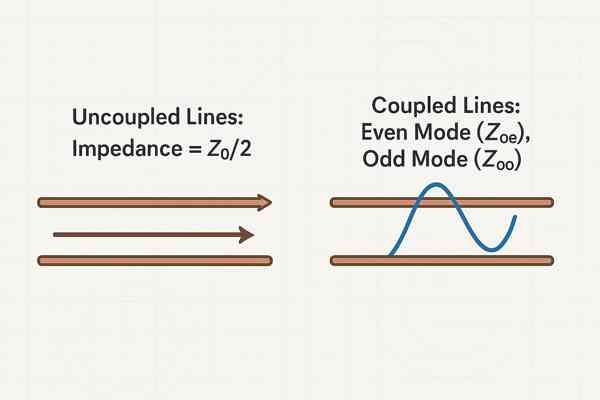
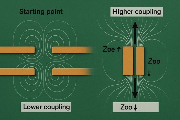
When two identical transmission lines of characteristic impedance \(Z_{0}\) are placed in parallel without significant coupling, their equivalent impedance is \(Z_{0}/2\). However, for high-frequency signals where lines are close enough to couple, the situation is described by even mode (\(Z_{oe}\)) and odd mode (\(Z_{oo}\)) impedances, which depend on the spacing between the lines.
It seems simple to just halve the impedance, but that's not the whole story. The interaction between the electromagnetic fields of the lines complicates things. As an engineer with nearly two decades of experience in high-tech hardware, I've seen how overlooking these details can derail a project. Let's break down this concept to ensure your designs are robust and reliable.
What is the Difference Between Characteristic Impedance and Input Impedance?
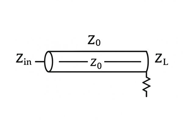
Ever mix up characteristic impedance and input impedance? It's an easy mistake. They sound similar but describe very different things, and confusing them can lead to nasty signal reflections in your circuits.
Characteristic impedance (\(Z_{0}\)) is a property of the transmission line itself, determined by its physical geometry and materials. Input impedance (\(Z_{in}\)) is what a signal source "sees" when looking into the line, and it depends on the characteristic impedance, the line's length, and the load impedance.
How \(Z_{0}\) and \(Z_{in}\) are Defined and Calculated
A great way to understand the difference is to compare them side-by-side.
| Feature | Characteristic Impedance1 (\(Z_{0}\)) | Input Impedance2 (\(Z_{in}\)) |
|---|---|---|
| Definition | Inherent impedance of a uniform, infinite line. | Impedance seen at the input of a finite line with a specific load. |
| Depends On | Physical geometry (\(W\), \(H\), \(t\)) and material (\(\epsilon_{r}\)). | \(Z_{0}\), load impedance (\(Z_{L}\)), and line length (\(l\)). |
| Varies with Length? | No, it's a constant property of the line's cross-section. | Yes, unless the line is perfectly matched (\(Z_{L} = Z_{0}\)). |
| Goal for Matching | Design the line's geometry to achieve a target \(Z_{0}\) (e.g., 50 \(\Omega\)). | Terminate the line with a load \(Z_{L} = Z_{0}\) to make \(Z_{in} = Z_{0}\). |
The key takeaway is that \(Z_{0}\) is something you design, while \(Z_{in}\) is the result of that design combined with your load. In a well-designed system, you make the input impedance equal to the characteristic impedance by matching the load.
How Do You Calculate the Characteristic Impedance of a Single Microstrip Transmission Line?
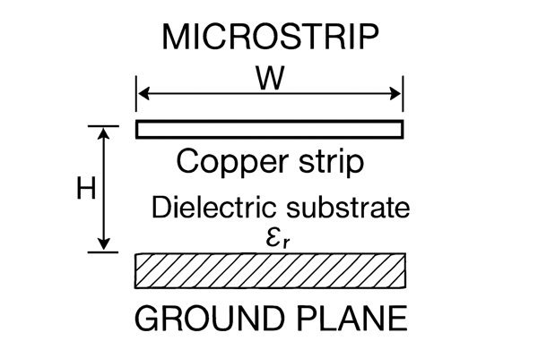
Need to design a 50-ohm trace on your PCB but don't know what width to use? Guessing the trace width can lead to impedance mismatches, causing signal integrity problems that are a headache to debug later.
The characteristic impedance (\(Z_{0}\)) of a microstrip line is calculated using well-established formulas, such as those from Wheeler or Hammerstad and Jensen. For example, for conditions where \(W/H \le 1\), Wheeler's classic equations first calculate the effective dielectric constant: \(\epsilon_{eff} \approx \frac{\epsilon_r + 1}{2} + \frac{\epsilon_r - 1}{2} \left( \frac{1}{\sqrt{1 + 12(H/W)}} + 0.04\left(1 - \frac{W}{H}\right)^2 \right)\). This is then used to find the impedance: \(Z_0 \approx \frac{60}{\sqrt{\epsilon_{eff}}} \ln\left(\frac{8H}{W} + \frac{W}{4H}\right)\).
Applying Wheeler's Equations for Microstrip Lines
While other highly accurate models from Hammerstad and Jensen exist, Wheeler's classic formulas provide an excellent and intuitive basis for calculation. A table of practical values using these equations offers a better feel for how impedance changes with geometry.
The following table shows calculated impedance values for a typical FR-4 PCB (Substrate Height \(H\) = 1.6 mm, \(\epsilon_{r}\) = 4.2, Trace Thickness \(t\) = 35 \(\mu\text{m}\)).
| Trace Width (\(W\)) | \(W/H\) Ratio | Effective \(\epsilon_{eff}\) | Characteristic Impedance (\(Z_{0}\)) |
|---|---|---|---|
| 1.0 mm | 0.625 | 3.19 | 75.1 \(\Omega\) |
| 2.0 mm | 1.25 | 3.42 | 59.2 \(\Omega\) |
| 3.0 mm | 1.875 | 3.58 | 50.1 \(\Omega\) |
| 4.0 mm | 2.50 | 3.69 | 44.1 \(\Omega\) |
| 5.0 mm | 3.125 | 3.77 | 39.7 \(\Omega\) |
As the table clearly shows, to achieve the industry-standard 50 \(\Omega\) impedance on a common 1.6 mm thick FR-4 board, you need a relatively wide trace of about 3.0 mm. This is why controlled impedance traces on thinner dielectric layers are often preferred in dense designs.
What Are the Effects of Coupling Between Parallel Transmission Lines?
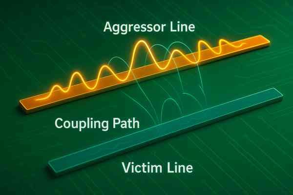
Are your parallel high-speed traces interfering with each other? This phenomenon, known as coupling or crosstalk, can corrupt your signals, causing bit errors and system failures. It's a major concern in dense PCB layouts.
When two transmission lines run parallel, their electromagnetic fields overlap. This interaction, or coupling, causes energy from one line (the aggressor) to be transferred to the other (the victim). The result is crosstalk, which manifests as noise on the victim line.
The Physics of Crosstalk3: Mutual Inductance4 and Capacitance
Coupling is governed by mutual capacitance5 (\(C_{m}\)) and mutual inductance (\(L_{m}\)). This interaction creates two distinct types of crosstalk noise on the victim trace.
| Crosstalk Type | Description | Direction of Travel on Victim Line |
|---|---|---|
| Near-End Crosstalk (NEXT) | Noise measured at the input of the victim line, near the aggressor source. | Travels backward, toward the source. |
| Far-End Crosstalk (FEXT) | Noise measured at the output of the victim line, far from the source. | Travels forward, with the signal. |
Generally, NEXT is the more significant of the two and is less dependent on the signal's rise time, making it a primary concern in PCB layout. The amount of coupling is directly related to how close the lines are and for how long they run in parallel.
How Does the Spacing Between Parallel Transmission Lines Affect Their Impedance?
Are you trying to pack differential pairs or parallel buses as tightly as possible? Be careful. The spacing between traces is one of the most critical factors determining their impedance and the amount of crosstalk.
As the spacing between two parallel transmission lines decreases, the mutual capacitance and mutual inductance increase. This stronger coupling causes the even mode impedance (\(Z_{oe}\)) to increase and the odd mode impedance (\(Z_{oo}\)) to decrease, significantly altering the line's behavior for differential and common-mode signals.
The "3W Rule" and a Quantitative Look at Spacing vs. Impedance
For single-ended signals, a common rule of thumb to minimize crosstalk is the "3W Rule". This rule states that the edge-to-edge separation between two traces should be at least three times the width of a single trace.
For coupled pairs, the spacing is a deliberate design choice. The table below shows the dramatic effect of spacing (\(S\)) on the impedances of a coupled pair (\(W\)=0.8mm, \(H\)=0.8mm, \(\epsilon_{r}\)=4.2, \(t\)=35\(\mu\text{m}\)).
| Spacing (\(S\)) | \(S/H\) Ratio | Even Mode Z (\(Z_{oe}\)) | Odd Mode Z (\(Z_{oo}\)) | Differential Z (\(Z_{diff}\)) |
|---|---|---|---|---|
| 1.6 mm | 2.0 | 75.1 \(\Omega\) | 60.5 \(\Omega\) | 121.0 \(\Omega\) |
| 0.8 mm | 1.0 | 82.3 \(\Omega\) | 50.1 \(\Omega\) | 100.2 \(\Omega\) |
| 0.4 mm | 0.5 | 91.5 \(\Omega\) | 41.2 \(\Omega\) | 82.4 \(\Omega\) |
| 0.2 mm | 0.25 | 102.7 \(\Omega\) | 34.0 \(\Omega\) | 68.0 \(\Omega\) |
As you can see, halving the spacing from 0.8 mm to 0.4 mm changes the differential impedance from a standard 100 \(\Omega\) to just 82.4 \(\Omega\). This demonstrates how critical spacing is for achieving your target impedance.
What is the Difference Between Even Mode and Odd Mode Impedance?
If you work with differential pairs, you've heard of even and odd mode impedance. But what do they really mean? Misunderstanding them leads to incorrect differential impedance calculations and failed signal integrity.
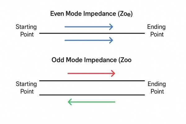
Even mode impedance (\(Z_{oe}\)) is the impedance of one line in a coupled pair when both lines are driven with the same signal (common mode). Odd mode impedance (\(Z_{oo}\)) is the impedance of one line when they are driven with equal and opposite signals (differential mode).
Visualizing Fields and Essential Formulas for \(Z_{oe}\) and \(Z_{oo}\)
The two modes behave very differently due to the interaction of their electromagnetic fields.
| Parameter | Even Mode | Odd Mode |
|---|---|---|
| Driving Signal | Same voltage & phase (common-mode). | Equal & opposite voltage (differential). |
| E-Field Lines | Primarily from traces to ground. | Strong field between the two traces. |
| Impedance | \(Z_{oe}\) (Higher, due to lower effective capacitance). | \(Z_{oo}\) (Lower, due to higher effective capacitance). |
| Relation to \(Z_{0}\) | \(Z_{oe} > Z_{0}\) | \(Z_{oo} < Z_{0}\) |
| Primary Use | Analyzing common-mode noise rejection. | Calculating the differential impedance (\(Z_{diff} = 2 \times Z_{oo}\)). |
The characteristic impedance of a single, isolated trace (\(Z_{0}\)) is the geometric mean of the even and odd mode impedances:
\(Z_{0} = \sqrt{Z_{oe} \times Z_{oo}}\)
These relationships are the key to designing and analyzing any coupled transmission line system.
How Do You Design a Power Divider Using Parallel Transmission Lines?
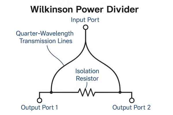
Need to split a high-frequency signal into two equal paths? Using a simple T-junction won't work well, as it creates impedance mismatches and provides no isolation between the output ports.
A Wilkinson Power Divider is a common and efficient circuit that uses quarter-wavelength transmission lines to split a signal while maintaining impedance match at all ports. A resistor placed between the output ports provides crucial isolation, preventing signals from one output from affecting the other.
Step-by-Step Design of a Wilkinson Power Divider
The design of a two-way Wilkinson divider6 is based on specific impedance transformations. The required values are straightforward and depend only on the system impedance \(Z_{0}\).
| System Impedance (\(Z_{0}\)) | Transformer Leg Impedance (\(Z_{0} \sqrt{2}\)) | Isolation Resistor Value (\(2 Z_{0}\)) |
|---|---|---|
| 50 \(\Omega\) (Standard RF) | 70.7 \(\Omega\) | 100 \(\Omega\) |
| 75 \(\Omega\) (Video/Cable) | 106.1 \(\Omega\) | 150 \(\Omega\) |
Here are the design rules:
- Input/Output Lines: The main input and the two output transmission lines must have the system's characteristic impedance, \(Z_{0}\).
- Quarter-Wave Transformers: The two parallel lines that form the split are not \(Z_{0}\). They must be designed for the impedance listed in the table above and have a physical length equal to one-quarter of the signal's wavelength (\(\lambda/4\)) in the substrate.
- Isolation Resistor: A resistor with the value from the table is placed directly between the two output ports.
How Do I Model Parallel Transmission Lines in Simulation Software (e.g., SPICE, ADS)?
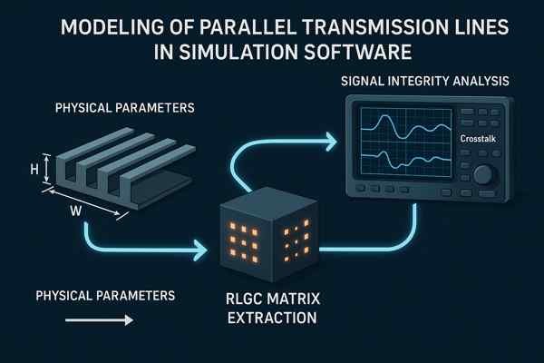
Need to predict the performance of your high-speed interconnects before fabrication? Accurately modeling parallel lines in simulation software is essential for analyzing signal integrity issues like crosstalk, reflections, and timing skew.
To model parallel lines, simulators like SPICE or Keysight ADS use multi-conductor transmission line models. These models are defined by physical parameters (\(W\), \(S\), \(H\)) or, more accurately, by an underlying RLGC (Resistance, Inductance, G-Conductance, Capacitance) matrix, which is typically extracted from a 2D or 3D field solver.
Specific Models and Workflow for ADS and SPICE
The approach and models used differ between the most common simulation tools.
| Feature | Keysight ADS | SPICE (HSPICE, LTspice, etc.) |
|---|---|---|
| Primary Model | MCLIN (microstrip), SCLIN (stripline) etc. | W-Element (lossy, multi-conductor) |
| Input Method | Enter physical geometry (\(W\), \(S\), \(H\), \(\epsilon_{r}\)). | Requires a pre-calculated RLGC matrix. |
| Underlying Engine | Built-in 2D Field Solver. | Solves circuit equations based on the provided matrix. |
| Best For | Integrated design & simulation environments. | System-level transient simulation with pre-characterized interconnects. |
For any serious high-speed design, the professional workflow is the same: 1. Design Geometry → 2. Field Solver Extraction (to get the RLGC matrix or S-parameters) → 3. Circuit Simulation.
Are There Online Calculators for Coupled Transmission Line Impedance?
Need a quick impedance calculation without firing up a full-blown field solver? Online calculators can be a great starting point for estimating coupled line impedance, but their accuracy varies widely.
Yes, numerous online calculators are available for coupled transmission line impedance. However, it is crucial to understand their underlying calculation method. Many free tools use simplified IPC-based formulas, while more advanced calculators may employ a 2D field solver for higher accuracy.
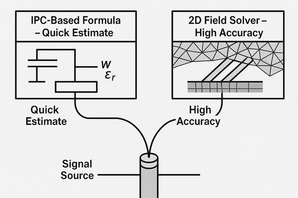
Evaluating Online Tools: Formula vs. Field Solver Accuracy
Choosing the right tool depends on the stage of your design.
| Calculator Type | Underlying Method | Accuracy | Best Use Case |
|---|---|---|---|
| Formula-Based | Analytical equations (e.g., IPC-2141). | Lower; less reliable for tight coupling. | Quick "what-if" scenarios, initial design. |
| 2D Field Solver-Based | Numerical solver (BEM/FEM). | High; often within 1-2% of 3D solvers. | Detailed design, final verification. |
As a practical recommendation, use formula-based calculators for a "first pass" design. For example, to quickly see if a 100-ohm differential impedance is even feasible with a given stackup. But for final verification before sending a board to fabrication, always rely on the integrated 2D field solver within your EDA tool or a dedicated tool like Polar SI90007.
Conclusion
In summary, the impedance of parallel lines is simple only when they are far apart. When close, coupling creates distinct even and odd mode impedances, which are critical for high-speed design.
-
Understanding characteristic impedance is crucial for designing efficient transmission lines and ensuring signal integrity. ↩
-
Exploring input impedance calculations can enhance your knowledge of circuit design and improve performance in various applications. ↩
-
Learn how crosstalk impacts PCB performance and discover strategies to minimize noise and interference in your circuit designs. ↩
-
Learn how mutual inductance contributes to crosstalk and why understanding it is crucial for effective PCB layout and signal integrity. ↩
-
Understanding mutual capacitance is crucial for designing circuits with minimal crosstalk, enhancing performance. ↩
-
Understanding the Wilkinson divider is crucial for RF design, as it optimizes power distribution and minimizes signal loss. ↩
-
Learn how Polar SI9000 provides highly accurate impedance calculations, essential for ensuring your PCB designs meet manufacturing requirements. ↩


