 Skip to content
Struggling with JTAG communication failures on your new board? You've checked the connections, but the debugger still won't connect. The problem might be your PCB layout and trace length.
The maximum recommended trace length for JTAG signals is typically under 6 inches (about \(15 \text{ cm}\)). This rule of thumb applies to standard TCK clock speeds up to \(25 \text{ MHz}\). For higher speeds, the traces must be significantly shorter to maintain signal integrity.

I've spent countless hours debugging boards where everything looked perfect electrically but failed functionally. Often, the root cause was a signal integrity issue hidden in the PCB layout, like a JTAG trace that was just a little too long. Understanding the limits and best practices is not just academic; it's what separates a working prototype from a frustrating paperweight. Let's break down the rules I follow to ensure my JTAG interfaces are robust and reliable every time.
What Are The General JTAG Layout Guidelines?
You've designed a complex board and left the JTAG layout as an afterthought. Now, you're facing intermittent connection issues that are impossible to pin down, delaying your entire bring-up process.
Keep JTAG traces as short and direct as possible, preferably under 6 inches. Route them over a solid ground plane, avoid noisy areas like switching regulators, and use a star topology from the connector to a single device or a clean daisy-chain for multiple devices.
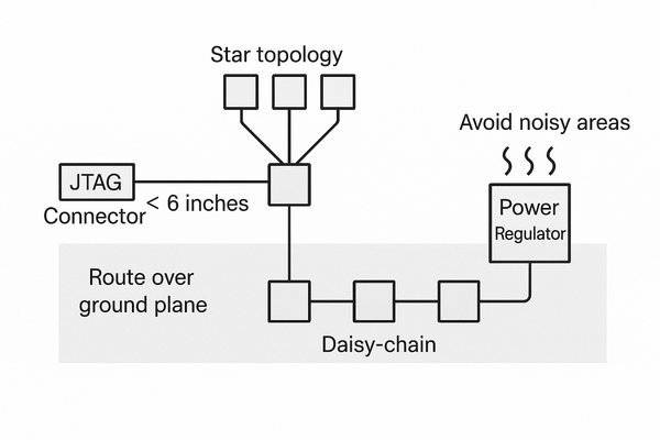
When I was leading the hardware design for a next-gen infusion pump, the JTAG was our lifeline for firmware development and testing. The first prototype had issues because the JTAG lines were routed around the board's edge, picking up noise from a motor driver. We learned our lesson fast. For the next revision, we treated the JTAG layout with the same respect as a high-speed interface, and the problems vanished. A little planning goes a long way.
Best Practices for Using Vias in JTAG Layouts
Each time a signal passes through a via, its impedance changes, creating a small reflection. While one or two vias are usually acceptable for a slow JTAG signal, using an excessive number can degrade the signal. More importantly, when a signal changes layers, its return current needs a path to follow. If the reference plane changes, the return current has to find another path, which can create a large current loop and significant noise.
Best Practice: Whenever you use a via on a JTAG signal (or any signal, really), place a ground "stitching" via as close as possible to it. This provides a direct, low-inductance path for the return current to follow the signal, preserving signal integrity.
Summary of JTAG Layout Best Practices
| Guideline | Recommendation | Why It Matters |
|---|---|---|
| Trace Length | Keep under 6 inches (\(15 \text{ cm}\)) for TCK \(\leq 25 \text{ MHz}\). Shorter is always better. | Minimizes signal degradation, reflections, and noise pickup. |
| Ground Plane | Route over a solid, continuous ground plane. | Ensures a low-inductance return path and stable impedance. |
| Signal Spacing | Maintain at least \(3\text{x}\) trace width spacing between JTAG and other signals. | Reduces crosstalk, especially from high-speed or noisy traces. |
| Avoid Noise | Keep JTAG traces far away from switching power supplies, clocks, and motors. | Prevents noise from coupling onto the JTAG lines and corrupting data. |
| Vias | Minimize the number of vias. Place a ground "stitching" via next to each signal via. | Vias create impedance discontinuities and disrupt the return path. |
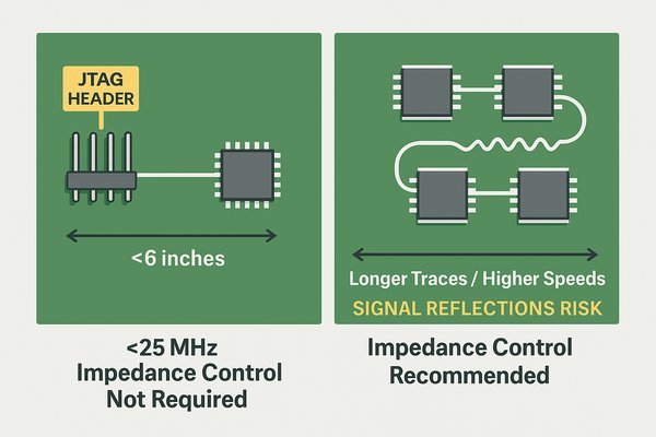
Do JTAG Signals Need To Be Impedance-Controlled?
Wondering if you need to pay extra for impedance control on your prototype PCB just for the JTAG lines? It feels like overkill, but you're worried about potential signal integrity problems.
For short traces (under 6 inches) and TCK speeds below \(25 \text{ MHz}\), impedance control is not strictly required. However, it is highly recommended for longer traces, higher speeds, or boards with multiple devices in a daisy chain to prevent signal reflections and ensure reliability.
On a high-pressure project for a photonic computing chip, the JTAG was the only way to access critical internal registers. We couldn't afford any risks, so we specified \(50 \Omega\) impedance control1 for the JTAG traces from day one. It’s a simple precaution that prevents a whole class of potential headaches.
The Impact of No Impedance Control
When a trace is not impedance-controlled, or its termination doesn't match, signal reflections occur. On an oscilloscope, this looks like overshoot and ringing. This ringing is dangerous because if it's severe enough to cross the logic threshold of the input pin multiple times, the component might register multiple false clock edges on the TCK line. This completely desynchronizes the JTAG state machine and causes communication to fail.
A Practical Decision Matrix for Impedance Control
Here's a simple guide to help you decide whether you need impedance control for your JTAG layout.
| TCK Speed | Trace Length | Recommendation | Rationale |
|---|---|---|---|
| Up to \(25 \text{ MHz}\) | \(< 3\) inches (\(7.5 \text{ cm}\)) | Not Required | Reflections are minimal and settle quickly. |
| Up to \(25 \text{ MHz}\) | \(3 - 6\) inches | Recommended | Good practice to ensure signal integrity. |
| \(> 25 \text{ MHz}\) | Any length | Mandatory | Fast edge rates will cause significant ringing. |
| Any Speed | \(> 6\) inches (\(15 \text{ cm}\)) | Mandatory | Long traces act as transmission lines. |
My personal rule is simple: if the trace is longer than 3 inches, I define it as a \(50 \Omega\) single-ended trace in the layout rules. It's a "do it and forget it" solution.
What Is The Recommended Characteristic Impedance For JTAG Traces?
You've decided to implement impedance control for your JTAG lines, but now you need to pick a value. Is it \(50 \Omega\), \(75 \Omega\), or something else? Choosing the wrong value could create new problems.
The industry-standard and most recommended characteristic impedance for JTAG traces is \(50 \Omega\). This value provides a good balance between signal integrity and driver capability and is widely supported by JTAG debugger pods, ICs, and termination components.
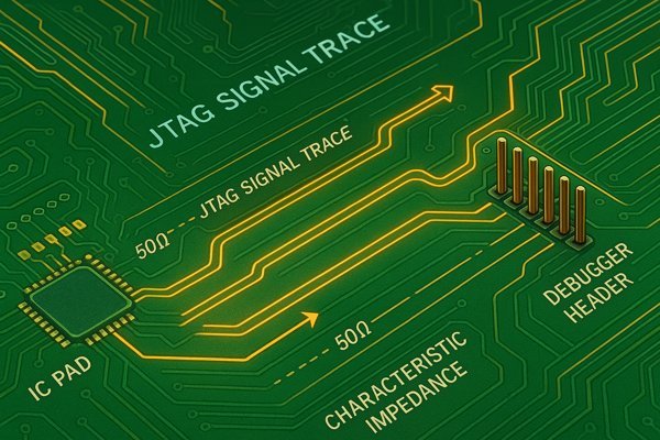
Why \(50 \Omega\)? It's a historical standard that emerged in RF and high-speed digital design. It represents a practical compromise: low enough to allow drivers to provide sufficient current without excessive power dissipation, yet high enough to not be overly sensitive to manufacturing variations. Every JTAG debugger I've ever used is designed with the assumption of a \(50 \Omega\) environment.
Choosing Between Microstrip and Stripline Routing
When defining impedance in your layout tool, you need to know if your trace is a microstrip or a stripline. The table below summarizes the key differences to help you choose.
| Feature | Microstrip (Outer Layer) | Stripline (Inner Layer) |
|---|---|---|
| PCB Layer | Top or Bottom | An internal signal layer |
| Reference Planes | One plane below the trace | Two planes (one above, one below) |
| Propagation Speed | Faster (dielectric is air & PCB material) | Slower (dielectric is only PCB material) |
| Noise Immunity | More susceptible to external noise | Excellent immunity, as the signal is shielded by the planes |
| Trace Width | Wider for the same impedance | Narrower for the same impedance |
For JTAG, either is acceptable, but routing on an internal layer as a stripline can offer better protection from external noise. For reference, a simplified formula for microstrip impedance (\(Z_{0}\)) is \(Z_{0} \approx \frac{87}{\sqrt{\epsilon_{r} + 1.41}} \ln\left(\frac{5.98H}{0.8W + T}\right)\), where \(\epsilon_{r}\) is the dielectric constant, and \(H\), \(W\), and \(T\) are physical dimensions of the trace and dielectric.
How to Specify Impedance Requirements to Your Fabricator
Always communicate your impedance requirements to your PCB fabricator. Typically, you specify "Create \(50 \Omega \pm 10\%\) single-ended traces for net class U_JTAG" in your fabrication notes. They will then adjust the final trace widths to hit that target precisely.
Should JTAG Signals Be Length-Matched?
You're meticulously routing your PCB and wondering if you need to add those serpentine squiggles to the JTAG lines to match their lengths, just like you would for a DDR interface. This adds complexity and takes up space.
No, JTAG signals do not need to be length-matched. The JTAG protocol is a relatively slow, synchronous interface where data is sampled on the edge of TCK. The timing margins are very generous, making minor differences in trace length irrelevant for proper operation.
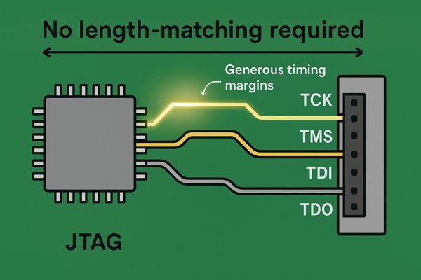
When designing high-speed memory interfaces like DDR4, I spend days ensuring that byte lanes are matched to within a few thousandths of an inch. But for JTAG, I don't even check the lengths. The reason lies in the protocol's timing budget. At a \(25 \text{ MHz}\) TCK speed, the clock period is a full \(40\) nanoseconds, while a 6-inch length mismatch only creates about \(1\) ns of skew, which is well within the timing margin of most devices.
Why JTAG Is Tolerant to Signal Skew
Length matching becomes critical in source-synchronous, high-speed parallel interfaces where multiple data lines are sampled on the same clock edge, and the data is only valid for a very short window. The table below illustrates why JTAG is different.
| Interface | Typical Speed | Length Matching Requirement | Why? |
|---|---|---|---|
| JTAG | \(10 - 50 \text{ MHz}\) | No | Large timing margins, slow protocol. |
| DDR3/DDR4 | \(800 - 2400+ \text{ MT/s}\) | Yes, critical (within a group) | Very small data valid window (sub-nanosecond). |
| PCIe | \(2.5 - 16+ \text{ GT/s}\) | Yes, critical (within a pair) | Differential pairs require precise matching to avoid EMI. |
| I2C/SPI | \(100 \text{ kHz} - 20+ \text{ MHz}\) | No | Similar to JTAG, these are slow synchronous protocols. |
Instead of spending time length-matching JTAG traces, focus your effort on keeping the overall trace lengths short and routing them cleanly.
How To Properly Route A JTAG Daisy Chain With Multiple Devices?
Your board has a CPU and an FPGA that both need JTAG access. You need to connect them both to a single JTAG header, but you're not sure about the correct wiring order for a daisy chain.
Connect the TDO (Test Data Out) of the first device to the TDI (Test Data In) of the second. Route TCK, TMS, and TRST in parallel to all devices. The TDI of the JTAG header connects to the first device's TDI, and the TDO of the last device connects back to the header's TDO.
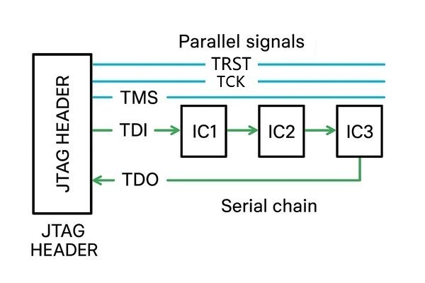
I remember designing a security system with four different processors on the same board. A daisy chain was the only practical solution. The key is to think of it as a single, long shift register. The data flows out of the debugger's TDI, through the first chip, then the second, and so on, before finally returning to the debugger's TDO pin.
Example Wiring Table for a JTAG Daisy Chain
Here is an explicit wiring table for a two-device chain (U1 and U2) that clarifies the connections.
| Source Pin | Destination Pin(s) | Notes |
|---|---|---|
| JTAG_HEADER.TDI | U1.TDI | Data enters the first device in the chain. |
| U1.TDO | U2.TDI | Data out of the first device feeds the second. |
| U2.TDO | JTAG_HEADER.TDO | Data from the last device returns to the debugger. |
| JTAG_HEADER.TCK | U1.TCK, U2.TCK | Clock signal is routed in parallel to both devices. |
| JTAG_HEADER.TMS | U1.TMS, U2.TMS | Mode select signal is routed in parallel. |
| JTAG_HEADER.TRST_N | U1.TRST_N, U2.TRST_N | Reset signal is routed in parallel. |
Using JTAG Buffers for Large or Complex Chains
As you add more devices to a JTAG chain, the total capacitive load on the TCK and TMS lines increases. A typical JTAG debugger can reliably drive 4-5 devices. Beyond that, or if the total trace length is very long, you should use a JTAG buffer or repeater IC. These chips receive the JTAG signals and re-drive them with a stronger, cleaner signal to the devices on the board.
How To Improve A Noisy JTAG Signal?
You've connected an oscilloscope to your JTAG lines and see a mess of ringing, overshoot, and noise. Your debugger connection is flaky at best. How can you clean up these signals and get a stable connection?
Start by lowering the TCK speed in your debugger software. If that works, you can fix the hardware by adding \(22 \Omega - 33 \Omega\) series termination resistors on TCK and TMS, ensuring a solid ground reference, and checking that all required pull-up/pull-down resistors are correctly placed.
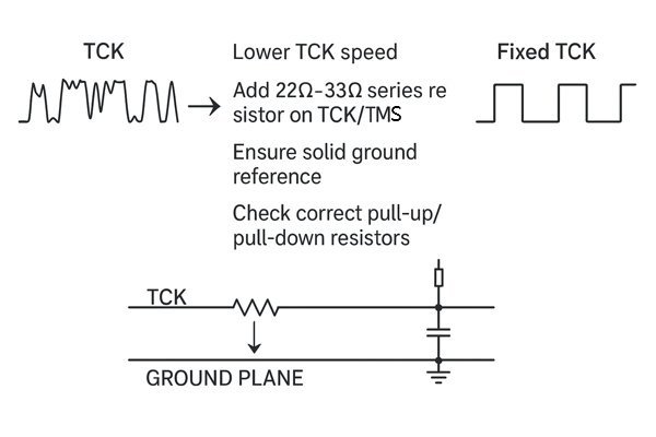
I once had to debug a prototype where JTAG communication would fail after a few seconds. Probing the TCK line showed massive overshoot—the signal was peaking at nearly \(5\text{V}\) on a \(3.3\text{V}\) interface! The fix was simple: I soldered a \(33 \Omega\) resistor in series with the TCK line right at the JTAG header. The overshoot disappeared, and the connection became rock solid.
A Troubleshooting Checklist for Noisy JTAG Signals
-
Slow Down the Clock: This is the easiest first step. In your debugger's settings, reduce the TCK frequency to \(100 \text{ kHz}\). If the connection becomes stable, you have confirmed a signal integrity problem.
-
Verify Pull Resistors: Double-check your schematic. Are all the necessary pull-up and pull-down resistors present and correctly valued?
-
Add Series Termination: Place a \(22 \Omega\) to \(33 \Omega\) resistor in series with the TCK line, as close to the JTAG header as possible. If problems persist, add the same termination to TMS and TDI.
-
Check the Ground Connection: Ensure your JTAG header has a solid ground pin connected directly to the board's main ground plane.
-
Review the Layout: Check for long traces, routes over splits in the ground plane, or proximity to noisy components.
-
Check Voltages: Confirm that the VREF pin on the JTAG header is connected to the target's I/O voltage.
How Does TCK Speed Affect Maximum Trace Length?
You understand that faster clock speeds require shorter traces, but you want to know the specific numbers. How long can your JTAG trace be if you run TCK at \(10 \text{ MHz}\) versus \(50 \text{ MHz}\)?
The relationship is inversely proportional: as TCK speed increases, the maximum allowable trace length decreases significantly. A trace that is fine at \(10 \text{ MHz}\) may fail completely at \(50 \text{ MHz}\) due to signal integrity issues caused by the faster signal edge rates.
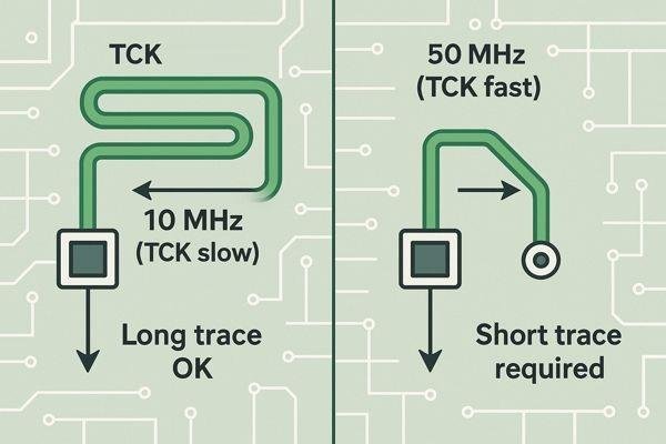
The key factor isn't the clock frequency itself, but the signal's rise time2. A \(50 \text{ MHz}\) clock from a modern debugger has very fast edges (\(< 1 \text{ ns}\)). These fast edges contain high-frequency harmonics that make the trace behave like a transmission line.
How "Critical Length" Determines When a Trace Needs Control
A trace behaves as a transmission line when its length is long enough that reflections can't settle before the next signal transition. For a typical \(1 \text{ ns}\) rise time, this "critical length" is around 3 inches. Any trace longer than this will likely experience problematic reflections if not properly terminated, regardless of the TCK frequency.
Recommended JTAG Trace Lengths by TCK Speed
This table provides practical guidelines based on this principle.
| TCK Frequency | Maximum Recommended Trace Length | Key Considerations |
|---|---|---|
| \(1 - 10 \text{ MHz}\) | Up to 12 inches (\(\approx 30 \text{ cm}\)) | Generally robust. Less sensitive to layout imperfections. Termination is optional but good practice. |
| \(10 - 25 \text{ MHz}\) | Under 6 inches (\(\approx 15 \text{ cm}\)) | This is the most common range. Good layout practices are important. Traces are at or above critical length. |
| \(25 - 50 \text{ MHz}\) | Under 4 inches (\(\approx 10 \text{ cm}\)) | Signal integrity is a primary concern. Series termination (\(22-33 \Omega\)) and \(50 \Omega\) impedance control are highly recommended. |
| \(> 50 \text{ MHz}\) | Under 2 inches (\(\approx 5 \text{ cm}\)) | This is high-speed design. Impedance control and termination are mandatory. A JTAG buffer is often required. |
What Are Common Causes Of JTAG Communication Failure?
You're staring at a "Failed to connect to target" error, and you've tried everything you can think of. What are the most common, overlooked issues that cause JTAG to fail?
The most common causes are hardware-related: incorrect or missing pull-up/pull-down resistors, especially on TRST. Other frequent culprits include poor signal integrity from long traces, incorrect daisy-chain wiring, and a missing VREF connection to the debugger.
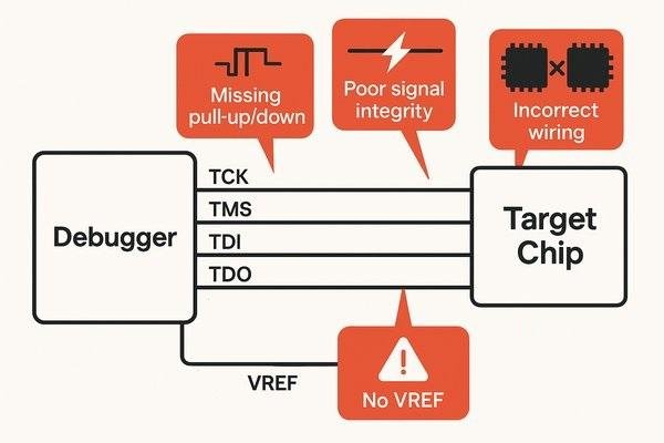
I can tell you that \(90\%\) of the time, the problem is not some complex software configuration but a simple, fundamental hardware mistake. The following table outlines a systematic approach to troubleshooting these common issues.
JTAG Troubleshooting Guide
| Common Problem | What to Check / How to Fix |
|---|---|
| Incorrect Pull Resistors | Verify schematic: Is TRST_N pulled HIGH to VCC via a \(1-10k\Omega\) resistor? Is TCK pulled LOW? Are TMS/TDI pulled HIGH? This is the #1 cause. |
| Power and VREF Issues | Verify voltage: Is the VREF pin on the JTAG header connected to the target's I/O voltage? Is the target board powered on? |
| Signal Integrity Issues | Lower TCK speed in your debugger. If it works, the issue is SI. Add series termination resistors (\(22-33\Omega\)) to fix it in hardware. |
| Incorrect Daisy-Chain Wiring | Trace the connections: Ensure TDO of one device goes to TDI of the next. Confirm the device order in software matches the PCB layout. |
| Mismatched I/O Voltages | Check datasheets: If a \(3.3\text{V}\) IC is in a chain with a \(1.8\text{V}\) IC, a level-shifter is required between them. A direct connection will fail. |
| Physical Connection Problems | Swap components: Try a different JTAG pod and ribbon cable. Inspect solder joints on the JTAG header under a microscope. |
Conclusion
Mastering JTAG layout isn't complex. Keep traces under 6 inches, use proper pull resistors, terminate when needed, and handle mixed-voltage chains carefully. These rules will ensure reliable communication and save debugging headaches.


